Oscillators: crystal oscillators

CRYSTAL OSCILLATORS

Crystal oscillators are those in which a specially-cut crystal controls the frequency. CRYSTAL- CONTROLLED OSCILLATORS are the standard means used for maintaining the frequency of radio transmitting stations within their assigned frequency limits. A crystal-controlled oscillator is usually used to produce an output which is highly stable and at a very precise frequency.

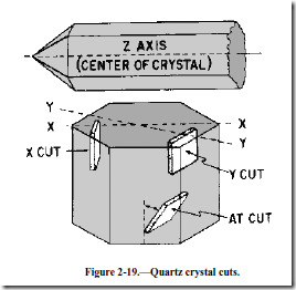
As stated earlier, crystals used in electrical circuits are thin sheets cut from the natural crystal and are ground to the proper thickness for the desired resonant frequency. For any given crystal cut, the thinner the crystal, the higher the resonant frequency. The "cut" (X, Y, AT, and so forth) of the crystal means the precise way in which the usable crystal is cut from the natural crystal. Some typical crystal cuts may be seen in figure 2-19.

imageTransmitters which require a very high degree of frequency stability, such as a broadcast transmitter, use temperature-controlled ovens to maintain a constant crystal temperature. These ovens are thermostatically controlled containers in which the crystals are placed.

The type of cut also determines the activity of the crystal. Some crystals vibrate at more than one frequency and thus will operate at harmonic frequencies. Crystals which are not of uniform thickness may have two or more resonant frequencies. Usually one resonant frequency is more pronounced than the others. The other less pronounced resonant frequencies are referred to as SPURIOUS frequencies. Sometimes such a crystal oscillates at two frequencies at the same time.

The amount of current that can safely pass through a crystal ranges from 50 to 200 milliamperes. When the rated current is exceeded, the amplitude of mechanical vibration becomes too great, and the crystal may crack. Overloading the crystal affects the frequency of vibration because the power dissipation and crystal temperature increase with the amount of load current.

Crystals as Tuned Circuits

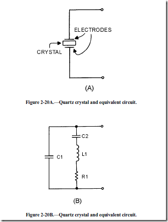
A quartz crystal and its equivalent circuit are shown in figure 2-20, views (A) and (B). Capacitor C2, inductor L1, and resistor R1 in view (B) represent the electrical equivalent of the quartz crystal in view (A). Capacitance C1 in (view B) represents the capacitance between the crystal electrodes in view (A). Depending upon the circuit characteristics, the crystal can act as a capacitor, an inductor, a series-tuned circuit, or a parallel-tuned circuit.

image

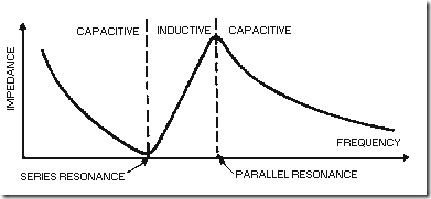
At some frequency, the reactances of equivalent capacitor C1 and inductor L will be equal and the crystal will act as a series-tuned circuit. A series-tuned circuit has a minimum impedance at resonance (figure 2-21). Above resonance the series-tuned circuit acts INDUCTIVELY, and below resonance it acts CAPACITIVELY. In other words, the crystal unit has its lowest impedance at the series-resonance frequency. The impedance increases as the frequency is lowered because the unit acts as a capacitor. The impedance of the crystal unit also increases as the frequency is raised above the series-resonant point because the unit acts as an inductor. Therefore, the crystal unit reacts as a series-tuned circuit.

clip_image007

Figure 2-21.—Frequency response of a crystal.

Since the series-tuned circuit acts as an inductor above the resonant point, the crystal unit becomes equivalent to an inductor and is parallel with the equivalent capacitor C1 (view (B) of figure 2-20). At some frequency above the series-resonant point, the crystal unit will act as a parallel-tuned circuit. A parallel-tuned circuit has a MAXIMUM impedance at the parallel-resonant frequency and acts inductively below parallel resonance (figure 2-21). Therefore, at some frequency, depending upon the cut of the crystal, the crystal unit will act as a parallel-tuned circuit.

The frequency stability of crystal-controlled oscillators depends on the Q of the crystal. The Q of a crystal is very high. It may be more than 100 times greater than that obtained with an equivalent electrical circuit. The Q of the crystal is determined by the cut, the type of holder, and the accuracy of grinding. Commercially produced crystals range in Q from 5,000 to 30,000 while some laboratory experiment crystals range in Q up to 400,000.

Crystal-Controlled Armstrong Oscillator

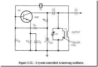
The crystal-controlled Armstrong oscillator (figure 2-22) uses the series-tuned mode of operation. It works much the same as the Hartley oscillator except that frequency stability is improved by the crystal (in the feedback path). To operate the oscillator at different frequencies, you simply change crystals (each crystal operates at a different frequency).

image

Variable capacitor C1 makes the circuit tunable to the selected crystal frequency. C1 is capable of tuning to a wide band of selected crystal frequencies. Regenerative feedback from the collector to base is through the mutual inductance between the transformer windings of T1. This provides the necessary 180-degree phase shift for the feedback signal. Resistors R B, RF, and RC provide the base and collector bias voltage. Capacitor CE bypasses ac variations around emitter resistor RE.

At frequencies above and below the series-resonant frequency of the selected crystal, the impedance of the crystal increases and reduces the amount of feedback signal. This, in turn, prevents oscillations at frequencies other than the series-resonant frequency.

Crystal-Controlled Pierce Oscillator

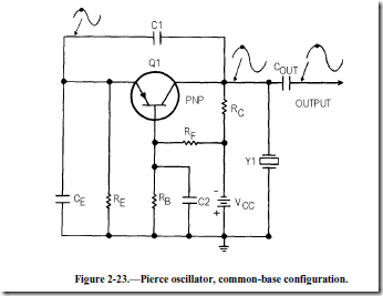
The crystal-controlled PIERCE OSCILLATOR uses a crystal unit as a parallel-resonant circuit. The Pierce oscillator is a modified Colpitts oscillator. They operate in the same way except that the crystal unit replaces the parallel-resonant circuit of the Colpitts.

Figure 2-23 shows the common-base configuration of the Pierce oscillator. Feedback is supplied from the collector to the emitter through capacitor C1. Resistors RB, RC, and RF provide the proper bias conditions for the circuit and resistor RE is the emitter resistor. Capacitors C1 and CE form a voltage divider connected across the output. Since no phase shift occurs in the common-base circuit, capacitor C1 feeds back a portion of the output signal to the emitter without a phase shift. The oscillating frequency is determined not only by the crystal but also by the parallel capacitance caused by capacitors C1 and CE. This parallel capacitance affects the oscillator frequency by lowering it. Any change in capacitance of either C1 or CE changes the frequency of the oscillator.

image

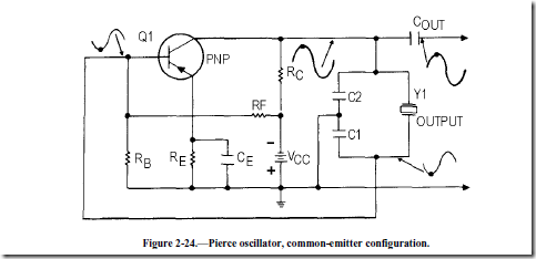
Figure 2-24 shows the common-emitter configuration of the Pierce oscillator. The resistors in the circuit provide the proper bias and stabilization conditions. The crystal unit and capacitors C1 and C2 determine the output frequency of the oscillator. The signal developed at the junction between Y1 and C1 is 180 degrees out of phase with the signal at the junction between Y1 and C2. Therefore, the signal at the Y1-C1 junction can be coupled back to the base of Q1 as a regenerative feedback signal to sustain oscillations.

image

Q-18. What is the impedance of a crystal at its resonant frequency when it is used in the parallel mode? Q-19. What is the impedance of a crystal at its resonant frequency when it is used in the series mode?


Oscillators: Hartley oscillator and resistive-capacitive (rc) feedback oscillator.

HARTLEY OSCILLATOR

The HARTLEY OSCILLATOR is an improvement over the Armstrong oscillator. Although its frequency stability is not the best possible of all the oscillators, the Hartley oscillator can generate a wide range of frequencies and is very easy to tune. The Hartley will operate class C with self-bias for ordinary operation. It will operate class A when the output waveform must be of a constant voltage level or of a linear wave shape. The two versions of this oscillator are the series-fed and the shunt-fed. The main difference between the Armstrong and the Hartley oscillators lies in the design of the feedback (tickler) coil. A separate coil is not used. Instead, in the Hartley oscillator, the coil in the tank circuit is a split inductor. Current flow through one section induces a voltage in the other section to develop a feedback signal.

Series-Fed Hartley Oscillator

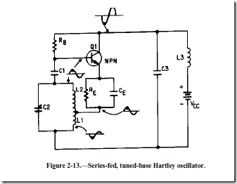
One version of a SERIES-FED HARTLEY OSCILLATOR is shown in figure 2-13. The tank circuit consists of the tapped coil (L1 and L2) and capacitor C2. The feedback circuit is from the tank circuit to the base of Q1 through the coupling capacitor C1. Coupling capacitor C1 prevents the low dc resistance of L2 from placing a short across the emitter-to-base junction and resistor RE. Capacitor C3 bypasses the sine-wave signal around the battery, and resistor RE is used for temperature stabilization to prevent thermal runaway. Degeneration is prevented by CE in parallel with RE. The amount of bias is determined by the values of RB, the emitter-to-base resistance, the small amount of dc resistance of coil L1, and the resistance of RE.

image

When a voltage is applied to the circuit, current from the battery flows through coil L1 and to the emitter through RE. Current then flows from the emitter to the collector and back to the battery. The surge of current through coil L1 induces a voltage in coil L2 to start oscillations within the tank circuit.

When current first starts to flow through coil L1, the bottom of L1 is negative with respect to the top of L2. The voltage induced into coil L2 makes the top of L2 positive. As the top of L2 becomes positive, the positive potential is coupled to the base of Q1 by capacitor C1. A positive potential on the base results in an increase of the forward bias of Q1 and causes collector current to increase. The increased collector current also increases the emitter current flowing through coil L1. Increased current through L1 results in more energy being supplied to the tank circuit, which, in turn, increases the positive potential at the top of the tank (L2) and increases the forward bias of Q1. This action continues until the rate of current change through coil L1 can no longer increase. The current through coil L1 and the transistor cannot continue increasing indefinitely, or the coil and transistor will burn up. The circuit must be designed, by proper selection of the transistor and associated parts, so that some point is reached when the current can no longer continue to increase. At this point C2 has charged to the potential across L1 and L2. This is shown as the heavy dot on the base waveform. As the current through L1 decreases, the voltage induced in L2 decreases. The positive potential across the tank begins to decrease and C2 starts discharging through L1 and L2. This action maintains current flow through the tapped coil and causes a decrease in the forward bias of Q1. In turn, this decrease in the forward bias of Q1 causes the collector and emitter current to decrease. At the instant the potential across the tank circuit decreases to 0, the energy of the tank circuit is contained in the magnetic field of the coil. The oscillator has completed a half cycle of operation.

Next, the magnetic field around L2 collapses as the current from C2 stops. The action of the collapsing magnetic field causes the top of L2 to become negative at this instant. The negative charge causes capacitor C2 to begin to charge in the opposite direction. This negative potential is coupled to the base of Q1, opposing its forward bias. Most transistor oscillators are operated class A; therefore, the positive and negative signals applied to the base of Q1 will not cause it to go into saturation or cutoff. When the tank circuit reaches its maximum negative value, the collector and the emitter currents will still be present but at a minimum value. The magnetic field will have collapsed and the oscillator will have completed 3/4 cycle.

At this point C2 begins to discharge, decreasing the negative potential at the top of L2 (potential will swing in the positive direction). As the negative potential applied to the base of Q1 decreases, the opposition to the forward bias also decreases. This, in effect, causes the forward bias to begin increasing, resulting in increased emitter current flowing through L1. The increase in current through L1 causes additional energy to be fed to the tank circuit to replace lost energy. If the energy lost in the tank is replaced with an equal or larger amount of energy, oscillations will be sustained. The oscillator has now completed 1 cycle and will continue to repeat it over and over again.

Shunt-Fed Hartley Oscillator

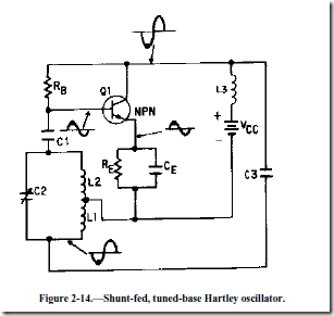
A version of a SHUNT-FED HARTLEY OSCILLATOR is shown in figure 2-14. The parts in this circuit perform the same basic functions as do their counterparts in the series-fed Hartley oscillator. The difference between the series-fed and the shunt-fed circuit is that dc does not flow through the tank circuit. The shunt-fed circuit operation is essentially the same as the series-fed Hartley oscillator. When voltage is applied to the circuit, Q1 starts conducting. As the collector current of Q1 increases, the change (increase) is coupled through capacitor C3 to the tank circuit, causing it to oscillate. C3 also acts as an isolation capacitor to prevent dc from flowing through the feedback coil. The oscillations at the collector will be coupled through C3 (feedback) to supply energy lost within the tank.

image

Q-12. What is the main difference between the Armstrong oscillator and the Hartley oscillator? Q-13. What is the difference between the series-fed and the shunt-fed Hartley oscillator? COLPITTS OSCILLATOR

Both the Armstrong and the Hartley oscillators have a tendency to be unstable in frequency because of junction capacitance. In comparison, the COLPITTS OSCILLATOR has fairly good frequency stability, is easy to tune, and can be used for a wide range of frequencies. The large value of split capacitance is in parallel with the junctions and minimizes the effect on frequency stability.

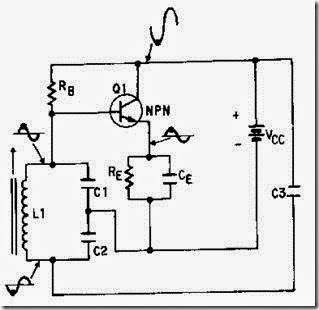
The Colpitts oscillator is very similar to the shunt-fed Hartley oscillator, except that two capacitors are used in the tank circuit instead of a tapped coil (figure 2-15). The Hartley oscillator has a tap between two coils, while the Colpitts has a tap between two capacitors. You can change the frequency of the Colpitts either by varying the inductance of the coil or by varying the capacitance of the two capacitors in the tank circuit. Notice that no coupling capacitor is used between the tank circuit and the base of Q1. Capacitors C1 and C2 of the tank circuit are in parallel with the input and the output interelement capacitance (capacitance between emitter, base, and collector) of the transistor. Thus the input and the output capacitive effect can be minimized on the tank circuit and better frequency stability can be obtained than with the Armstrong or the Hartley oscillator.

clip_image006

Figure 2-15.—Colpitts oscillator.

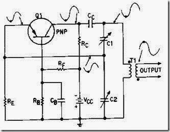
Figure 2-16 shows a common-base Colpitts oscillator using a pnp transistor as the amplifying device. Notice in this version of the Colpitts oscillator that regenerative feedback is obtained from the tank circuit and applied to the emitter. Base bias is provided by resistor RB and RF. Resistor R C is the collector load resistor. Resistor RE develops the input signal and also acts as the emitter swamping resistor. The tuned circuit consists of C1 and C2 in parallel with the primary winding of transformer T1. The voltage developed across C2 is the feedback voltage. Either or both capacitors may be adjusted to control the frequency. In the common-base configuration there is no phase difference between the signal at the collector and the emitter signal. Therefore, the phase of the feedback signal does not have to be changed. When the emitter swings negative, the collector also swings negative and C2 charges negatively at the junction of C1 and C2. This negative charge across C2 is fed back to the emitter. This increases the reverse bias on Q1. The collector of Q1 becomes more negative and C2 charges to a negative potential. This feedback effect continues until the collector of Q1 is unable to become any more negative. At that time the primary of T1 will act as a source because of normal tank circuit operation. As its field collapses, the tank potential will reverse and C1 and C2 will begin to discharge. As C2 becomes less negative, the reverse bias on Q1 decreases and its collector voltage swings in the positive direction. C1 and C2 will continue to discharge and then charge in a positive direction. This positive-going voltage across C2 will be fed back to the emitter as regenerative feedback. This will continue until the field around the primary of T1 collapses. At that time the collector of Q1 will be at a maximum positive value. C1 and C2 will begin to discharge and the potential at their junction will become less positive. This increases the reverse bias on Q1 and drives the collector negative, causing C1 and C2 to charge in a negative direction and to repeat the cycle.

clip_image008

Figure 2-16.—Common-base Colpitts oscillator.

Q-14. What is the identifying feature of a Colpitts oscillator?

RESISTIVE-CAPACITIVE (RC) FEEDBACK OSCILLATOR

As mentioned earlier, resistive-capacitive (RC) networks provide regenerative feedback and determine the frequency of operation in RESISTIVE-CAPACITIVE (RC) OSCILLATORS.

The oscillators presented in this chapter have used resonant tank circuits (LC). You should already know how the LC tank circuit stores energy alternately in the inductor and capacitor.

The major difference between the LC and RC oscillator is that the frequency-determining device in the RC oscillator is not a tank circuit. Remember, the LC oscillator can operate with class A or C biasing because of the oscillator action of the resonant tank. The RC oscillator, however, must use class A biasing because the RC frequency-determining device doesn’t have the oscillating ability of a tank circuit.

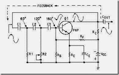
An RC FEEDBACK or PHASE-SHIFT oscillator is shown in figure 2-17. Components C1, R1, C2, R2, C3, and RB are the feedback and frequency-determining network. This RC network also provides the needed phase shift between the collector and base.

clip_image010

Figure 2-17.—Phase-shift oscillator.

Phase-Shift Oscillators

The PHASE-SHIFT OSCILLATOR, shown in figure 2-17, is a sine-wave generator that uses a resistive-capacitive (RC) network as its frequency-determining device.

As discussed earlier in the common-emitter amplifier configuration (figure 2-17), there is a 180-degree phase difference between the base and the collector signal. To obtain the regenerative feedback in the phase-shift oscillator, you need a phase shift of 180 degrees between the output and the input signal. An RC network consisting of three RC sections provides the proper feedback and phase inversion to provide this regenerative feedback. Each section shifts the feedback signal 60 degrees in phase.

Since the impedance of an RC network is capacitive, the current flowing through it leads the applied voltage by a specific phase angle. The phase angle is determined by the amount of resistance and capacitance of the RC section.

If the capacitance is a fixed value, a change in the resistance value will change the phase angle. If the resistance could be changed to zero, we could get a maximum phase angle of 90 degrees. But since a voltage cannot be developed across zero resistance, a 90-degree phase shift is not possible.

With a small value of resistance, however, the phase angle or phase shift is less than 90 degrees. In the phase-shift oscillator, therefore, at least three RC sections are needed to give the required 180-degree phase shift for regenerative feedback. The values of resistance and capacitance are generally chosen so that each section provides about a 60-degree phase shift.

Resistors RB, RF, and RC provide base and collector bias. Capacitor C E bypasses ac variations around the emitter resistor R E. Capacitors C1, C2, and C3 and resistors R1, R2, and R B form the feedback and phase-shifting network. Resistor R2 is variable for fine tuning to compensate for any small changes in value of the other components of the phase-shifting network.

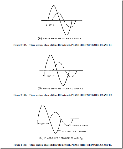
When power is applied to the circuit, oscillations are started by any random noise (random electrical variations generated internally in electronic components). A change in the flow of base current results in an amplified change in collector current which is phase-shifted the 180 degrees. When the signal is returned to the base, it has been shifted 180 degrees by the action of the RC network, making the circuit regenerative. View (A) of figure 2-18 shows the amount of phase shift produced by C1 and R1. View (B) shows the amount of phase shift produced by C2 and R2 (signal received from C1 and R1), and view (C) shows the complete phase shift as the signal leaves the RC network. With the correct amount of resistance and capacitance in the phase-shifting network, the 180-degree phase shift occurs at only one frequency. At any other than the desired frequency, the capacitive reactance increases or decreases and causes an incorrect phase relationship (the feedback becomes degenerative). Thus, the oscillator works at only one frequency. To find the resonant frequency (fr) of an RC phase shift oscillator, use the following formula:

clip_image011

where n is the number of RC sections.

image

A high-gain transistor must be used with the three-section RC network because the losses in the network are high. Using more than three RC sections actually reduces the overall signal loss within the network. This is because additional RC sections reduce the phase shift necessary for each section, and the loss for each section is lowered as the phase shift is reduced. In addition, an oscillator that uses four or more RC networks has more stability than one that uses three RC networks. In a four-part RC network, each part shifts the phase of the feedback signal by approximately 45 degrees to give the total required 180-degree phase shift.

Q-15. Which components provide the regenerative feedback signal in the phase-shift oscillator? Q-16. Why is a high-gain transistor used in the phase-shift oscillator?

Q-17. Which RC network provides better frequency stability, three-section or four-section?


Oscillators: frequency stability, amplitude stability and Armstrong oscillator.

  FREQUENCY STABILITY

The FREQUENCY STABILITY of an oscillator is a measure of the degree to which a constant frequency output is approached. The better the frequency stability, the closer the output will be to a constant frequency.

Frequency INSTABILITY (variations above and below the desired output frequency) may be caused by transistor characteristics or by variations in the external circuit elements.

As stated before, when output power is not of prime importance, transistor oscillators may be biased class A to ensure stability and minimize distortion. When this is done, the dc operating point established by the power supply is chosen so that the operation of the transistor oscillator occurs over the most linear portion of the transistor’s characteristic curve. When the operation of the circuit falls into the nonlinear portion of the characteristic curve, the transistor’s parameters (voltages and currents) vary. These parameters are basic to the stable frequency of the transistor oscillator. Operating frequency variations may occur with changes in these bias voltages. Thus, a constant supply voltage is a prime requirement for good frequency stability.

The use of a common bias source for both collector and emitter electrodes results in a relatively constant ratio of the two voltages. In effect, a change in one voltage is somewhat counteracted by the change in the other. This counteraction takes place because an increase in collector voltage causes an increase in the oscillating frequency, and an increase in emitter voltage causes a decrease in the oscillating frequency. This is a result of the change in capacitance between the junctions of the transistor. However, a common bias source does not completely compensate since the effects on other circuit parameters of each bias voltage differ.

Just as in any transistor circuit, changes in the transistor operating point and changes in temperature are encountered in the transistor oscillator. The effects of changes in temperature are to cause collector current to increase if the transistor is not stabilized. The increase in collector current can be prevented by reducing the forward bias.

AMPLITUDE STABILITY

The AMPLITUDE STABILITY of a transistor oscillator indicates the amount by which the actual output amplitude varies from the desired output amplitude.

The same parameters (voltages and currents) that affect frequency stability also affect amplitude stability. Output amplitude may be kept relatively constant by ensuring that the feedback is large enough that the collector current is maintained at the proper level. Feedback used in this manner makes the output voltage directly proportional to the supply voltage. Thus, regulation of the supply voltage ensures good amplitude stability.

ARMSTRONG OSCILLATOR

The ARMSTRONG OSCILLATOR is used to produce a sine-wave output of constant amplitude and of fairly constant frequency within the rf range. It is generally used as a local oscillator in receivers, as a source in signal generators, and as a radio-frequency oscillator in the medium- and high-frequency range.

The identifying characteristics of the Armstrong oscillator are that (1) it uses an LC tuned circuit to establish the frequency of oscillation, (2) feedback is accomplished by mutual inductive coupling between the tickler coil and the LC tuned circuit, and (3) it uses a class C amplifier with self-bias. Its frequency is fairly stable, and the output amplitude is relatively constant.

Views (A), (B), and (C) shown in figure 2-10 can be used to build the basic Armstrong oscillator. View (A) shows a conventional amplifier. R2 provides the forward bias for Q1, C2 is a coupling capacitor, and L1 and R1 form the collector load impedance. This is a common-emitter configuration which provides the 180-degree phase shift between the base and collector.

image_thumb[3]

image_thumb[4]

View (B) shows the frequency-determining device composed of inductor L2 and capacitor C1. C1 is a variable tuning capacitor which is used to adjust the resonant frequency to the desired value.

View (C) is the feedback network which uses L1 (the collector load) as the primary and L2 as the secondary winding of a coupling transformer to provide a 180-degree phase shift. Variable resistor R1 controls the amount of current through L1. When R1 is adjusted for maximum resistance, most of the current flows through L1. The transformer now couples a maximum signal which represents a large feedback amplitude into the tank circuit (L2, C1). If R1 is adjusted for a smaller resistance, less current flows through L1, and less energy is coupled to the tank circuit; therefore, feedback amplitude decreases. R1 is normally adjusted so that the L1 current is adequate to sustain tank oscillations.

View (D) shows the complete oscillator circuit. Connecting the feedback network through coupling capacitor C2 to the base of Q1 forms a "closed loop" for feedback (shown by the solid arrows). Let’s verify that the feedback is regenerative. Assume a positive signal on the base of Q1. The transistor conducts heavily when forward biased. This current flow through L1 and R1 causes the voltage across L1 to increase. The voltage increase is inductively coupled to L2 and inverted. This action ensures that the voltage is positive at the base end of L2 and C1 and in phase with the base voltage. The positive signal is now coupled through C2 to the base of Q1. The regenerative feedback offsets the damping in the frequency-determining network and has sufficient amplitude to provide unity circuit gain.

The circuit in view (D) has all three requirements for an oscillator: (1) amplification, (2) a frequency- determining device, and (3) regenerative feedback. The oscillator in this schematic drawing is a tuned- base oscillator, because the fdd is in the base circuit. If the fdd were in the collector circuit, it would be a tuned-collector oscillator. The circuit in view (D) is basically an Armstrong oscillator.

Refer to figure 2-10, view (D), for the following discussion of the circuit operation of the Armstrong oscillator. When VCC is applied to the circuit. a small amount of base current flows through R2 which sets the forward bias on Q1. This forward bias causes collector current to flow from ground through Q1, R1, and L1 to +VCC. The current through L1 develops a magnetic field which induces a voltage into the tank circuit. The voltage is positive at the top of L2 and C1. At this time, two actions occur. First, resonant tank capacitor C1 charges to this voltage; the tank circuit now has stored energy. Second, coupling capacitor C2 couples the positive signal to the base of Q1. With a positive signal on its base, Q1 conducts harder. With Q1 conducting harder, more current flows through L1, a larger voltage is induced into L2, and a larger positive signal is coupled back to the base of Q1. While this is taking place, the frequency- determining device is storing more energy and C1 is charging to the voltage induced into L2.

The transistor will continue to increase in conduction until it reaches saturation. At saturation, the collector current of Q1 is at a maximum value and cannot increase any further. With a steady current through L1, the magnetic fields are not moving and no voltage is induced into the secondary.

With no external voltage applied, C1 acts as a voltage source and discharges. As the voltage across C1 decreases, its energy is transferred to the magnetic field of L2. Now, let’s look at C2.

The coupling capacitor, C2, has charged to approximately the same voltage as C1. As C1 discharges, C2 discharges. The primary discharge path for C2 is through R2 (shown by the dashed arrow). As C2 discharges, the voltage drop across R2 opposes the forward bias on Q1 and collector current begins to decrease. This is caused by the decreasing positive potential at the base of Q1.

A decrease in collector current allows the magnetic field of L1 to collapse. The collapsing field of L1 induces a negative voltage into the secondary which is coupled through C2 and makes the base of Q1 more negative. This, again, is regenerative action; it continues until Q1 is driven into cutoff.

When Q1 is cut off, the tank circuit continues to flywheel, or oscillate. The flywheel effect not only produces a sine-wave signal, but it aids in keeping Q1 cut off. Without feedback, the oscillations of L2 and C1 would dampen out after several cycles.

To ensure that the amplitude of the signal remains constant, regenerative feedback is supplied to the tank once each cycle, as follows: As the voltage across C1 reaches maximum negative, C1 begins discharging toward 0 volts. Q1 is still below cutoff. C1 continues to discharge through 0 volts and becomes positively charged. The tank circuit voltage is again coupled to the base of Q1, so the base voltage becomes positive and allows collector current to flow. The collector current creates a magnetic

field in L1, which is coupled into the tank. This feedback action replaces any lost energy in the tank circuit and drives Q1 toward saturation. After saturation is reached, the transistor is again driven into cutoff.

The operation of the Armstrong oscillator is basically this: Power applied to the transistor allows energy to be applied to the tank circuit causing it to oscillate. Once every cycle, the transistor conducts for a short period of time (class C operation) and returns enough energy to the tank to ensure a constant amplitude output signal.

Class C operation has high efficiency and low loading characteristics. The longer Q1 is cut off, the less the loading on the frequency-determining device.

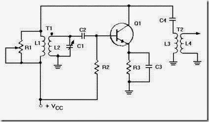
Figure 2-11 shows a tuned-base Armstrong oscillator as you will probably see it. R3 has been added to improve temperature stability. Bypass capacitor C3 prevents degeneration. C4 is an output coupling capacitor, and impedance-matching transformer T2 provides a method of coupling the output signal. T2 is usually a loosely coupled rf transformer which reduces undesired reflected impedance from the load back to the oscillator.

clip_image022_thumb

Figure 2-11.—Tuned-base Armstrong oscillator.

The Armstrong oscillator is an example of how a class C amplifier can produce a sine-wave output that is not distorted. Although class C operation is nonlinear and many harmonic frequencies are generated, only one frequency receives enough gain to cause the circuit to oscillate. This is the frequency of the resonant tank circuit. Thus, high efficiency and an undistorted output signal can be obtained.

The waveforms in figure 2-12 illustrate the relationship between the collector voltage and collector current. Notice that collector current (IC) flows for only a short time during each cycle. While the tank circuit is oscillating (figure 2-11), L2 acts as the primary of the transformer and L1 acts as the secondary. The signal from the tank is, therefore, coupled through T1 to coupling capacitor C4, and the output voltage across L4 is a sine wave.

image_thumb[5]


Oscillators: solid-state lc oscillators, feedback,types of feedback, configuration of oscillators, common-collector configuration, common-base configuration, common-emitter configuration and oscillator circuits.

SOLID-STATE LC OSCILLATORS

As you have just studied, a basic oscillator can be broken down into three main sections: a frequency-determining device, an amplifier, and a feedback circuit. The frequency-determining device in an LC oscillator is usually an LC tank circuit. Although the tank circuit is normally found in the input circuit of an oscillator (both electron tube and transistor), it sometimes appears in the output circuit. The differences in magnitude of plate and collector currents and shunting impedances are considerations in the designed locations of such tank circuits. In both solid-state and electron tube circuits, oscillations take place in the tuned circuit. Both the electron tube and the transistor function primarily as electrical valves that amplify and automatically deliver to the input circuit the proper amount of energy to sustain oscillations. In both tube and transistor oscillators, the feedback circuit couples energy of the proper amount and of the correct phase from the output to the input circuit to sustain oscillations.

FEEDBACK

Let’s review what you have studied up to this point concerning feedback. Feedback is the process of transferring energy from a high-level point in a system to a low-level point in a system. This means transferring energy from the output of an amplifier back to its input. If the output feedback signal opposes the input signal, the signal is DEGENERATIVE or NEGATIVE FEEDBACK. However, if the feedback aids the input signal, the feedback is REGENERATIVE or POSITIVE FEEDBACK. Regenerative or positive feedback is one of the requirements to sustain oscillations in an oscillator. This feedback can be applied in any of several ways to produce a practical oscillator circuit.

TYPES OF FEEDBACK

Chapter 1 described the resonant or tank circuit and how a sinusoidal signal is generated by the action of an inductor and a capacitor. The feedback signal is coupled from this circuit by either of two means. The first method is to take some of the energy from the inductor. This can be done by any one of the three ways shown in figure 2-7, views (A), (B), and (C). When an oscillator uses a TICKLER COIL, as shown in view (A), it is referred to as an ARMSTRONG OSCILLATOR. When an oscillator uses a tapped coil (view (B)) or a split coil (view (C)), it is referred to as a HARTLEY OSCILLATOR. The second method of coupling the feedback signal is to use two capacitors in the tank circuit and tap the feedback signal between them. This is shown in view (D). An oscillator using this method is referred to as a COLPITTS OSCILLATOR. Each of these particular oscillators is named after the person who originally designed them.

image

CONFIGURATION OF OSCILLATORS

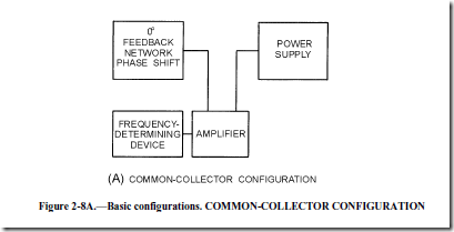
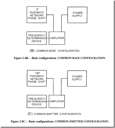
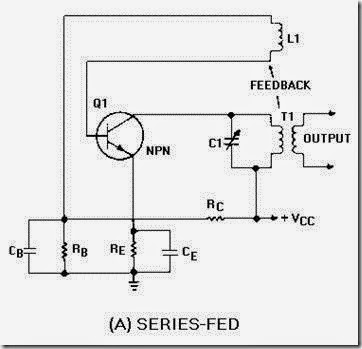
Any of the three basic amplifier configurations (common collector, common base, or common emitter) described in NEETS, Module 7, Introduction to Solid-State Devices and Power Supplies, Chapter 2, may be used for the oscillator circuit. However, certain considerations in the application of the circuit, such as the operating frequency and output power required, usually determine which of the three configurations is to be used. The three basic configurations are shown in figure 2-8, views (A), (B), and (C).

image

image

COMMON-COLLECTOR CONFIGURATION

Since there is no phase reversal between the input and output circuits of a common-collector configuration, the feedback network does not need to provide a phase shift. However, since the voltage gain is less than unity and the power gain is low, the common-collector configuration is very seldom used in oscillator circuits.

COMMON-BASE CONFIGURATION

The power gain and voltage gain of the common-base configuration are high enough to give satisfactory operation in an oscillator circuit. The wide range between the input resistance and the output resistance make impedance matching slightly harder to achieve in the common-base circuit than in the common-emitter circuit. An advantage of the common-base configuration is that it exhibits better high- frequency response than does the common-emitter configuration.

COMMON-EMITTER CONFIGURATION

The common-emitter configuration has high power gain and is used in low-frequency applications. For the energy which is fed back from the output to be in phase with the energy at the input, the feedback network of a common-emitter oscillator must provide a phase shift of approximately 180 degrees. An

advantage of the common-emitter configuration is that the medium resistance range of the input and output simplifies the job of impedance matching.

Q-6. What type of feedback aids an input signal?

Q-7. What are the two methods used for feedback coupling? Q-8. Which oscillator uses a tickler coil for feedback?

Q-9. Which oscillator uses a tapped inductor for feedback? Q-10. Which oscillator uses tapped capacitors for feedback?

Q-11. What are the three basic configurations of transistor oscillators?

OSCILLATOR CIRCUITS

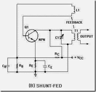
Oscillators may be classified by name, such as Armstrong, Hartley, Colpitts, or by the manner in which dc power is applied. An oscillator in which dc power is supplied to the transistor through the tank circuit, or a portion of the tank circuit, is said to be SERIES FED. An oscillator which receives its dc power for the transistor through a path separate and parallel to the tank circuit is said to be PARALLEL FED OR SHUNT FED. All the oscillators in this chapter can be constructed either way, series or shunt fed. The construction depends on the characteristics of the oscillator circuit the designer is interested in.

A SERIES-FED, TUNED-COLLECTOR ARMSTRONG OSCILLATOR is illustrated in figure 2-9,

view (A). The dc path is from the negative side (ground) of VCC through RE, Q1, T1, and back to the positive side of VCC. The figure clearly illustrates that both the ac and dc components flow through the tank circuit.

clip_image010

Figure 2-9A.—Series- and shunt-fed, tuned-collector Armstrong oscillators. SERIES-FED.

By modifying the circuit slightly, it becomes a SHUNT-FED, TUNED-COLLECTOR ARMSTRONG OSCILLATOR as shown in view (B). The dc component flows from ground through RE to Q1 to positive VCC. The dc is blocked from the tank circuit by capacitor C2. Only the ac component flows in the tank circuit.

clip_image012

Figure 2-9B.—Series- and shunt-fed, tuned-collector Armstrong oscillators. SHUNT-FED.

The function of an oscillator is to produce a sinusoidal waveshape of a specific frequency and amplitude. In doing so, the stability of an oscillator is very important. Depending on its application, an oscillator may be required to have either good frequency stability or amplitude stability; in many circumstances, both are required. Of the two, good frequency stability is usually considered more important.


Oscillators: classification of oscillators (generators), the basic oscillator and sine-wave oscillator.

OSCILLATORS
LEARNING OBJECTIVES

Upon completion of this chapter you will be able to:

1. List the two broad classifications of oscillators (wave generators).

2. Identify the three frequency-determining devices for sine-wave oscillators.

3. Describe the differences between series-fed and shunt-fed oscillators.

4. Explain how the crystal is equivalent to the series and parallel LC circuit.

5. Identify the Armstrong oscillator.

6. Identify the Hartley oscillator.

7. Identify the Colpitts oscillator.

8. Identify the resistive-capacitive oscillator.

9. Determine the frequency of a resistive-capacitive oscillator.

10. Explain the operation of a pulsed oscillator.

11. Determine how many cycles are present in the output of a pulsed oscillator.

12. Explain how frequency multiplication takes place.

INTRODUCTION

WAVE GENERATORS play a prominent role in the field of electronics. They generate signals from a few hertz to several gigahertz (109 hertz). Modern wave generators use many different circuits and generate such outputs as SINUSOIDAL, SQUARE, RECTANGULAR, SAWTOOTH, and TRAPEZOIDAL waveshapes. These waveshapes serve many useful purposes in the electronic circuits you will be studying. For example, they are used extensively throughout the television receiver to reproduce both picture and sound.

One type of wave generator is known as an OSCILLATOR. An oscillator can be regarded as an amplifier which provides its own input signal. Oscillators are classified according to the waveshapes they produce and the requirements needed for them to produce oscillations.

CLASSIFICATION OF OSCILLATORS (GENERATORS)

Wave generators can be classified into two broad categories according to their output waveshapes, SINUSOIDAL and NONSINUSOIDAL.

Sinusoidal Oscillators

A sinusoidal oscillator produces a sine-wave output signal. Ideally, the output signal is of constant amplitude with no variation in frequency. Actually, something less than this is usually obtained. The degree to which the ideal is approached depends upon such factors as class of amplifier operation, amplifier characteristics, frequency stability, and amplitude stability.

Sine-wave generators produce signals ranging from low audio frequencies to ultrahigh radio and microwave frequencies. Many low-frequency generators use resistors and capacitors to form their frequency-determining networks and are referred to as RC OSCILLATORS. They are widely used in the audio-frequency range.

Another type of sine-wave generator uses inductors and capacitors for its frequency-determining network. This type is known as the LC OSCILLATOR. LC oscillators, which use tank circuits, are commonly used for the higher radio frequencies. They are not suitable for use as extremely low-frequency oscillators because the inductors and capacitors would be large in size, heavy, and costly to manufacture.

A third type of sine-wave generator is the CRYSTAL-CONTROLLED OSCILLATOR. The crystal- controlled oscillator provides excellent frequency stability and is used from the middle of the audio range through the radio frequency range.

Nonsinusoidal Oscillators

Nonsinusoidal oscillators generate complex waveforms, such as square, rectangular, trigger, sawtooth, or trapezoidal. Because their outputs are generally characterized by a sudden change, or relaxation, they are often referred to as RELAXATION OSCILLATORS. The signal frequency of these oscillators is usually governed by the charge or discharge time of a capacitor in series with a resistor. Some types, however, contain inductors that affect the output frequency. Thus, like sinusoidal oscillators, both RC and LC networks are used for determining the frequency of oscillation. Within this category of nonsinusoidal oscillators are MULTIVIBRATORS, BLOCKING OSCILLATORS, SAWTOOTH GENERATORS, and TRAPEZOIDAL GENERATORS.

THE BASIC OSCILLATOR

An oscillator can be thought of as an amplifier that provides itself (through feedback) with an input signal. By definition, it is a nonrotating device for producing alternating current, the output frequency of which is determined by the characteristics of the device. The primary purpose of an oscillator is to generate a given waveform at a constant peak amplitude and specific frequency and to maintain this waveform within certain limits of amplitude and frequency.

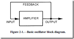
An oscillator must provide amplification. Amplification of signal power occurs from input to output. In an oscillator, a portion of the output is fed back to sustain the input, as shown in figure 2-1. Enough power must be fed back to the input circuit for the oscillator to drive itself as does a signal generator. To cause the oscillator to be self-driven, the feedback signal must also be
image

REGENERATIVE (positive). Regenerative signals must have enough power to compensate for circuit losses and to maintain oscillations.

Since a practical oscillator must oscillate at a predetermined frequency, a FREQUENCY- DETERMINING DEVICE (fdd), sometimes referred to as a FREQUENCY-DETERMINING NETWORK (fdn), is needed. This device acts as a filter, allowing only the desired frequency to pass. Without a frequency-determining device, the stage will oscillate in a random manner, and a constant frequency will not be maintained.

Before discussing oscillators further, let’s review the requirements for an oscillator. First, amplification is required to provide the necessary gain for the signal. Second, sufficient regenerative feedback is required to sustain oscillations. Third, a frequency-determining device is needed to maintain the desired output frequency.

The basic oscillator requirements, in addition to the application, determine the type of oscillator to be used. Let’s consider some factors that account for the complexity and unique characteristics of oscillators.

Virtually every piece of equipment that uses an oscillator has two stability requirements, AMPLITUDE STABILITY and FREQUENCY STABILITY. Amplitude stability refers to the ability of the oscillator to maintain a constant amplitude in the output waveform. The more constant the amplitude of the output waveform, the better the amplitude stability. Frequency stability refers to the ability of the oscillator to maintain its operating frequency. The less the oscillator varies from its operating frequency, the better the frequency stability.

A constant frequency and amplitude can be achieved by taking extreme care to prevent variations in LOAD, BIAS, and COMPONENT CHARACTERISTICS. Load variations can greatly affect the amplitude and frequency stability of the output of an oscillator. Therefore, maintaining the load as constant as possible is necessary to ensure a stable output.

As you should know from your study of transistor biasing, bias variations affect the operating point of the transistor. These variations may alter the amplification capabilities of the oscillator circuits as well. A well-regulated power supply and a bias-stabilizing circuit are required to ensure a constant, uniform signal output.

As a result of changing temperature and humidity conditions, the value or characteristics of components such as capacitors, resistors, and transistors can change. The changes in these components also cause changes in amplitude and frequency.

Output power is another consideration in the use of oscillators. Generally speaking, high power is obtained at some sacrifice to stability. When both requirements are to be met, a low-power, stable oscillator can be followed by a higher-power BUFFER AMPLIFIER. The buffer provides isolation between the oscillator and the load to prevent changes in the load from affecting the oscillator.

If the oscillator stage must develop high power, efficiency becomes important. Many oscillators use class C bias to increase efficiency. Other types of oscillators may use class A bias when a high efficiency is not required but distortion must be kept at a minimum. Other classes of bias may also be used with certain oscillators.

SINE-WAVE OSCILLATOR

RC networks, LC tanks, and crystals may appear in sine-wave oscillator circuits. An amplifier can be made into a sine-wave oscillator by providing regenerative feedback through an RC network.

RC Network

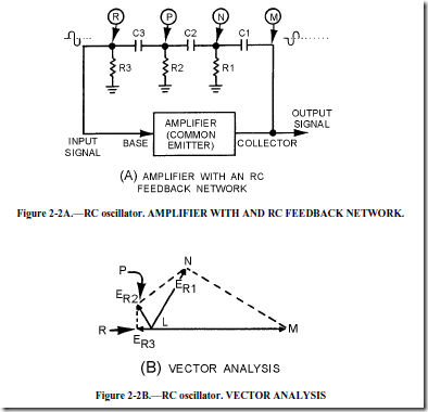
Figure 2-2, view (A), shows the block diagram of an amplifier with an RC network through which regenerative feedback is provided. The RC network also acts as the frequency-determining device. View

(B) shows a vector analysis of the signal E at various points in the circuit.
image

To analyze the operation of the circuit in view (A), assume that the amplifier is a common-emitter configuration. The signal on the collector (M) is 180 degrees out of phase with the signal (input) on the base (R). For the circuit to produce regenerative feedback, the RC network must provide a 180-degree phase shift of the collector signal. When power is applied to the circuit, a noise voltage (noise contains many different frequencies) will appear on the collector. This noise signal is represented by vector LM in view (B). As the signal couples through C1 and across R1 (view (A)), a phase shift occurs. The voltage across R1 (E R1), represented by vector LN, has been shifted in phase (about 60 degrees) and reduced in amplitude. The signal at point N (view (A)) is then coupled to the next RC section (R2 and C2). Using the same size resistor and capacitor as before will cause another 60-degree phase shift to take place. The signal at point P is the voltage across R2, represented by vector LP. Now the signal at point P has been shifted about 120 degrees and its amplitude is reduced still further. The same actions occur for the last section (R3 and C3). This signal experiences another 60-degree phase shift and has further amplitude reduction. The signal at point R (ER3) has been shifted 180 degrees and is represented by vector LR.

Notice that point R is the input to the base of the common-emitter amplifier. Also, vector LR shows that the signal on the base is regenerative (aiding the circuit operation). This meets the regenerative feedback requirement. An exact 60-degree phase shift per stage is not required, but the sum of the three phase shifts must equal 180 degrees.

For a given RC network, only one frequency of the initial noise signal will be shifted exactly 180 degrees. In other words, the network is frequency selective. Therefore, the RC network is the frequency- determining device since the lengths of the vectors and their phase relationships depend on frequency. The frequency of oscillations is governed by the values of resistance and capacitance in these sections. Variable resistors and capacitors may be used to provide tuning in the feedback network to allow for minor variations in phase shift. For an RC phase-shift oscillator, the amplifier is biased for class A operation to minimize distortion of the wave or signal.

LC Network

Some sine-wave oscillators use resonant circuits consisting of inductance and capacitance. For example, recall the tank circuit in which a resonant circuit stores energy alternately in the inductor and capacitor, producing a sine wave. You studied this action of the tank circuit in chapter 1.

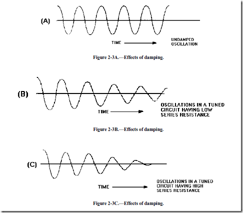
If there were absolutely no internal resistances in a tank circuit, oscillations would continue indefinitely, as shown in figure 2-3, view (A). Each resonant circuit does, however, contain some resistance which dissipates power. This power loss causes the amplitude to decrease, as shown in views (B) and (C). The reduction of amplitude in an oscillator circuit is referred to as DAMPING. Damping is caused by both tank and load resistances. The larger the tank resistance, the greater the amount of damping. Loading the tank causes the same effect as increasing the internal resistance of the tank. The effect of this damping can be overcome by applying regenerative feedback.
image

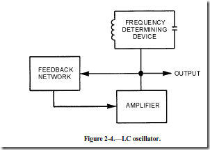
Figure 2-4 shows a block diagram of a typical LC oscillator. Notice that the oscillator contains the three basic requirements for sustained oscillations: amplification, a frequency-determining device, and regenerative feedback.
image

The amplifier supplies energy to begin what is known as the FLYWHEEL EFFECT. The flywheel effect is the maintenance of oscillations in a circuit in the intervals between pulses of excitation energy. Recall that in chapter 1 the tank circuit alternately stored energy in the inductor and capacitor. The LC network provides initial oscillations. A portion of the output of the LC network is then returned to the input of the amplifier through the regenerative-feedback network to sustain the oscillations.

When a tank circuit is used to develop oscillations in an oscillator, the output frequency of the oscillator is primarily the resonant frequency of the tank circuit and can be found by the formula:

clip_image014

Crystals

Another frequency-determining device is the CRYSTAL. The crystal may be used with a tank circuit, or it may perform alone. Crystals exhibit a characteristic known as the PIEZOELECTRIC EFFECT. The piezoelectric effect is the property of a crystal by which mechanical forces produce electrical charges and, conversely, electrical charges produce mechanical forces. This effect is a form of oscillation similar to the flywheel effect of a tank circuit.

The piezoelectric effect can be seen in a number of crystal substances. The most important of these are the minerals quartz and Rochelle salt. Although quartz does not exhibit the piezoelectric effect to the degree that Rochelle salt does, quartz is used for frequency control in oscillators because of its greater mechanical strength. Another mineral, tourmaline, is physically strong like quartz; but because it is more expensive, it is not used extensively as an fdd. This discussion will deal only with the quartz crystal.

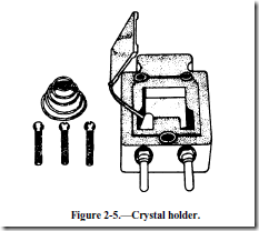
The crystals used in oscillator circuits are thin sheets, or wafers, cut from natural or synthetic quartz and ground to a specific thickness to obtain the desired resonant frequency. The crystals are mounted in holders, which support them physically and provide electrodes by which voltage is applied. The holder must allow the crystals freedom for vibration. There are many different types of holders. One type is shown in figure 2-5.
image

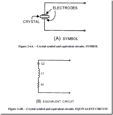
The frequency for which a crystal is ground is referred to as the NATURAL RESONANT FREQUENCY of the crystal. Voltage applied to the crystal produces mechanical vibrations which, in turn, produce an output voltage at the natural resonant frequency of the crystal. A vibrating crystal can be represented by an equivalent electrical circuit composed of capacitance, inductance, and resistance.

Figure 2-6, view (A), illustrates the symbol of a crystal; view (B) shows an equivalent circuit for the crystal. View (C) shows an equivalent circuit for the crystal and the holder; C1 represents the capacitance between the metal plates of the holder.
image

The Q (discussed in chapter 1) of a crystal is many times greater than that of an LC tank circuit. The high Q is present because the resistance in the crystal is extremely small. Commercially produced crystals range in Q from 5,000 to 30,000. The high Q causes the frequency stability to be much greater than that of an ordinary LC tank circuit. This is the reason a crystal is used in many sine-wave generator circuits.

Q-1. What are the two classifications of wave generators according to their output waveshapes?

Q-2. What are the three networks used for frequency-determining devices?

Q-3. What is another name for nonsinusoidal oscillators?

Q-4. What is a nonrotating device that produces alternating current?

Q-5. What are the three requirements necessary for oscillations to exist in a circuit?


Answers to questions and summary of tuned circuits.

SUMMARY

This chapter introduced you to the principles of tuned circuits. The following is a summary of the major subjects of this chapter.

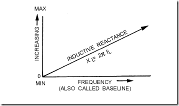
THE EFFECT OF FREQUENCY on an INDUCTOR is such that an increase in frequency will cause an increase in inductive reactance. Remember that XL = 2pfL; therefore, XL varies directly with frequency.

image

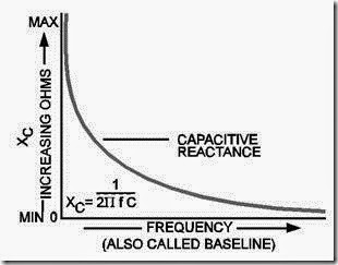
THE EFFECT OF FREQUENCY on a CAPACITOR is such that an increase in frequency will cause a decrease in capacitive reactance. Remember that

clip_image003

therefore, the relationship between XC and frequency is that XC varies inversely with frequency.

clip_image005

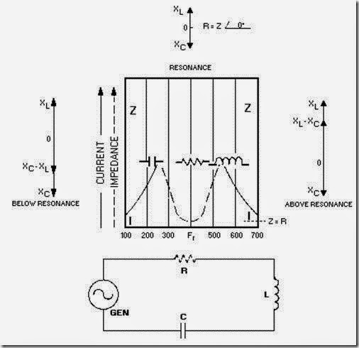
RESULTANT REACTANCE X = (XL – X C) or X = (XC – XL). XL is usually plotted above the reference line and X C below the reference line. Inductance and capacitance have opposite effects on the current in respect to the voltage in a.c. circuits. Below resonance, XC is larger than XL, and the series circuit appears capacitive. Above resonance, XL is larger than XC, and the series circuit appears inductive. At resonance, XL = XC, and the total impedance of the circuit is resistive.

A RESONANT CIRCUIT is often called a TANK CIRCUIT. It has the ability to take energy fed from a power source, store the energy alternately in the inductor and capacitor, and produce an output which is a continuous a.c. wave. The number of times this set of events occurs per second is called the resonant frequency of the circuit. The actual frequency at which a tank circuit will oscillate is determined by the formula:

clip_image006

IN A SERIES-LC CIRCUIT impedance is minimum and current is maximum. Voltage is the variable, and voltage across the inductor and capacitor will be equal but of opposite phases at resonance. Above resonance it acts inductively, and below resonance it acts capacitively.

clip_image008

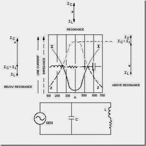
IN A PARALLEL-LC CIRCUIT impedance is maximum and current is minimum. Current is the variable and at resonance the two currents are 180 degrees out of phase with each other. Above resonance the current acts capacitively, and below resonance the current acts inductively.

clip_image010

THE "Q" OR FIGURE OF MERIT of a circuit is the ratio of XL to R. Since the capacitor has negligible losses, the circuit Q becomes equivalent to the Q of the coil.

clip_image011

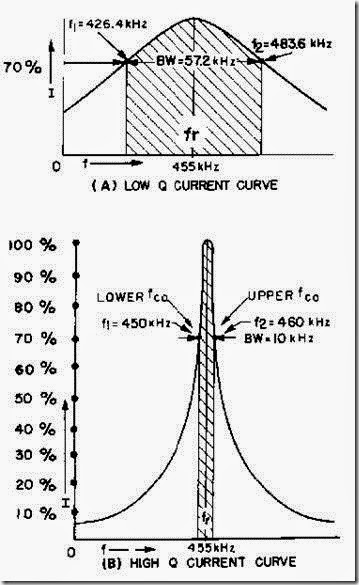
THE BANDWIDTH of a circuit is the range of frequencies between the half-power points. The limiting frequencies are those at either side of resonance at which the curve falls to .707 of the maximum value. If circuit Q is low, you will have a wide bandpass. If circuit Q is high, you will have a narrow bandpass.

clip_image013

A FILTER CIRCUIT consists of a combination of capacitors, inductors, and resistors connected so that the filter will either permit or prevent passage of a certain band of frequencies.

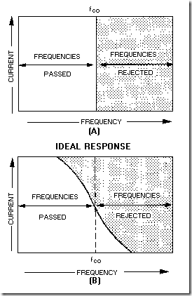
A LOW-PASS FILTER passes low frequencies and attenuates high frequencies.

clip_image014

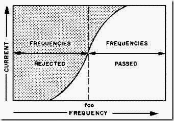
A HIGH-PASS FILTER passes high frequencies and attenuates low frequencies.

clip_image016

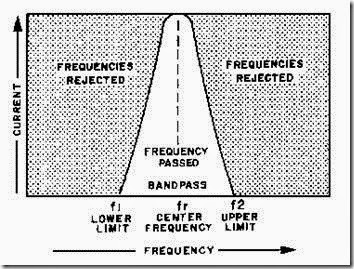
A BANDPASS FILTER will permit a certain band of frequencies to be passed.

clip_image018

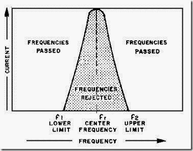
A BAND-REJECT FILTER will reject a certain band of frequencies and pass all others.

clip_image020

A SAFETY PRECAUTION concerning series resonance: Very high reactive voltage can appear across L and C. Care must be taken against possible shock hazard.

ANSWERS TO QUESTIONS Q1. THROUGH Q21.

A-1.

a. XL varies directly with frequency.

X L = 2pfL

b. XC varies inversely with frequency.

clip_image021

c. Frequency has no affect on resistance.

A-2. Resultant reactance. A-3.

clip_image022

A-4. Decreases.

A-5. Impedance low Current high.

A-6. Nonresonant (circuit is either above or below resonance).

A-7. Inductor magnetic field.

A-8. Capacitor.

A-9. Natural frequency or resonant frequency (f r).

A-10. Maximum impedance, minimum current.

A-11. At the resonant frequency. A-12.

clip_image023

A-13. Bandwidth of the circuit.

A-14. A filter.

A-15.

a. Low-pass.

b. High-pass

c. Bandpass.

d. Band-reject.

A-16. High-pass filter, low-frequency discriminator, or low-frequency attenuator.

A-17. Low-pass filter, high-frequency discriminator or high-frequency attenuator.

A-18. At low-frequency, a capacitor acts as an open and an inductor acts as a short. At high-frequency, a capacitor acts as a short and an inductor acts as an open.

A-19. Frequency cutoff (fco).

A-20. Bandpass.

A-21. Band-reject.