Wave shaping: nonsinusoidal voltages applied to an rc circuit and rc integrators.

Nonsinusoidal Voltages Applied to an RC Circuit

The harmonic content of a square wave must be complete to produce a pure square wave. If the harmonics of the square wave are not of the proper phase and amplitude relationships, the square wave will not be pure. The term PURE, as applied to square waves, means that the waveform must be perfectly square.

Figure 4-28 shows a pure square wave that is applied to a series-resistive circuit. If the values of the two resistors are equal, the voltage developed across each resistor will be equal; that is, from one pure square-wave input, two pure square waves of a lower amplitude will be produced. The value of the resistors does not affect the phase or amplitude relationships of the harmonics contained within the square waves. This is true because the same opposition is offered by the resistors to all the harmonics presented. However, if the same square wave is applied to a series RC circuit, as shown in figure 4-29, the circuit action is not the same.

clip_image002

Figure 4-28.—Square wave applied to a resistive circuit.

clip_image004

Figure 4-29.—Square wave applied to an RC circuit.

RC INTEGRATORS

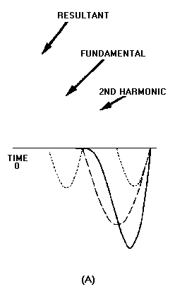
The RC INTEGRATOR is used as a waveshaping network in communications, radar, and computers. The harmonic content of the square wave is made up of odd multiples of the fundamental frequency. Therefore SIGNIFICANT HARMONICS (those that have an effect on the circuit) as high as 50 or 60 times the fundamental frequency will be present in the wave. The capacitor will offer a reactance (XC) of a different magnitude to each of the harmonics

clip_image005

This means that the voltage drop across the capacitor for each harmonic frequency present will not be the same. To low frequencies, the capacitor will offer a large opposition, providing a large voltage drop across the capacitor. To high frequencies, the reactance of the capacitor will be extremely small, causing a small voltage drop across the capacitor. This is no different than was the case for low- and high- pass filters (discriminators) presented in chapter 1. If the voltage component of the harmonic is not developed across the reactance of the capacitor, it will be developed across the resistor, if we observe Kirchhoff’s voltage law. The harmonic amplitude and phase relationship across the capacitor is not the same as that of the original frequency input; therefore, a perfect square wave will not be produced across the capacitor. You should remember that the reactance offered to each harmonic frequency will cause a change in both the amplitude and phase of each of the individual harmonic frequencies with respect to the current reference. The amount of phase and amplitude change taking place across the capacitor depends on the XC of the capacitor. The value of the resistance offered by the resistor must also be considered here; it is part of the ratio of the voltage development across the network.

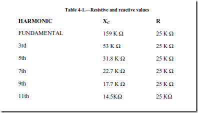
The circuit in figure 4-30 will help show the relationships of R and XC more clearly. The square wave applied to the circuit is 100 volts peak at a frequency of 1 kilohertz. The odd harmonics will be 3 kilohertz, 5 kilohertz, 7 kilohertz, etc. Table 4-1 shows the values of XC and R offered to several

harmonics and indicates the approximate value of the cutoff frequency (XC = R). The table clearly shows that the cutoff frequency lies between the fifth and seventh harmonics. Between these two values, the capacitive reactance will equal the resistance. Therefore, for all harmonic frequencies above the fifth, the majority of the output voltage will not be developed across the output capacitor. Rather, most of the output will be developed across R. The absence of the higher order harmonics will cause the leading edge of the waveform developed across the capacitor to be rounded. An example of this effect is shown in figure 4-31. If the value of the capacitance is increased, the reactances to each harmonic frequency will be further decreased. This means that even fewer harmonics will be developed across the capacitor.

clip_image007

Figure 4-30.—Partial integration circuit.

clip_image009

Figure 4-31.—Partial integration.

image

The harmonics not effectively developed across the capacitor must be developed across the resistor to satisfy Kirchhoff’s voltage law. Note the pattern of the voltage waveforms across the resistor and capacitor. If the waveforms across both the resistor and the capacitor were added graphically, the resultant would be an exact duplication of the input square wave.

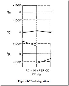
When the capacitance is increased sufficiently, full integration of the input signal takes place in the output across the capacitor. An example of complete integration is shown in figure 4-32 (waveform eC). This effect can be caused by significantly decreasing the value of capacitive reactance. The same effect would take place by increasing the value of the resistance. Integration takes place in an RC circuit when the output is taken across the capacitor..

image

The amount of integration is dependent upon the values of R and C. The amount of integration may also be dependent upon the time constant of the circuit. The time constant of the circuit should be at least 10 TIMES GREATER than the time duration of the input pulse for integration to occur. The value of 10 is only an approximation. When the time constant of the circuit is 10 or more times the value of the duration of the input pulse, the circuit is said to possess a long time constant. When the time constant is long, the capacitor does not have the ability to charge instantly to the value of the applied voltage. Therefore, the result is the long, sloping, integrated waveform.

Q18. What are the requirements for an integration circuit? Q19. Can a pure sine wave be integrated? Why?


Wave shaping: dual-diode limiter, clampers, series rc circuits, positive-diode clampers and negative-diode clampers.

DUAL-DIODE LIMITER

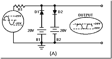
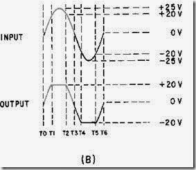
The last type of limiter to be discussed in this chapter is the DUAL-DIODE LIMITER, shown in figure 4-15, view (A). This limiter combines a parallel-negative limiter with negative bias (D1 and B1) and a parallel-positive limiter with positive bias (D2 and B2). Parts of both the positive and negative alternations are removed in this circuit. Each battery aids the reverse bias of the diode in its circuit; the circuit has no current flow with no input signal. When the input signal is below the value of the biasing batteries, both D1 and D2 are reverse biased. With D1 and D2 reverse biased, the output follows the input. When the input signal becomes more positive than +20 volts (view (B)), D2 conducts and limits the output to +20 volts. When the input signal becomes more negative than -20 volts, D1 conducts and limits the output to this, value. When neither diode conducts, the output follows the input waveform.

clip_image001

Figure 4-15A.—Dual-diode limiter.

clip_image003

Figure 4-15B.—Dual-diode limiter.

CLAMPERS

Certain applications in electronics require that the upper or lower extremity of a wave be fixed at a specific value. In such applications, a CLAMPING (or CLAMPER) circuit is used. A clamping circuit clamps or restrains either the upper or lower extremity of a waveform to a fixed dc potential. This circuit is also known as a DIRECT-CURRENT RESTORER or a BASE-LINE STABILIZER. Such circuits are used in test equipment, radar systems, electronic countermeasure systems, and sonar systems. Depending upon the equipment, you could find negative or positive clampers with or without bias. Figure 4-16, views (A) through (E), illustrates some examples of waveforms created by clampers. However, before we discuss clampers, we will review some relevant points about series RC circuits.

clip_image005

Figure 4-16A.—Clamping waveforms. WITHOUT CLAMPING.

clip_image007

Figure 4-16B.—Clamping waveforms. WITH CLAMPING, LOWER EXTREMITY OF WAVE IS HELD AT 0V.

clip_image009

Figure 4-16C.—Clamping waveforms. WITH CLAMPING, LOWER EXTREMITY OF WAVE IS HELD AT

+100 V.

clip_image011

Figure 4-16D.—Clamping waveforms. WITH CLAMPING, UPPER EXTREMITY OF WAVE IS HELD AT 0V.

clip_image013

Figure 4-16E.—Clamping waveforms. WITH CLAMPING, UPPER EXTREMITY OF WAVE IS HELD AT100 V.

SERIES RC CIRCUITS

Series RC circuits are widely used for coupling signals from one stage to another. If the time constant of the coupling circuit is comparatively long, the shape of the output waveform will be almost identical to that of the input. However, the output dc reference level may be different from that of the input. Figure 4-17, view (A), shows a typical RC coupling circuit in which the output reference level has been changed to 0 volts. In this circuit, the values of R1 and C1 are chosen so that the capacitor will charge (during T0 to T1) to 20 percent of the applied voltage, as shown in view (B). With this in mind, let’s consider the operation of the circuit.

clip_image015

Figure 4-17A.—RC coupling.

clip_image017

Figure 4-17B.—RC coupling.

At T0 the input voltage is -50 volts and the capacitor begins charging. At the first instant the voltage across C is 0 and the voltage across R is -50 volts. As C charges, its voltage increases. The voltage across R, which is the output voltage, begins to drop as the voltage across C increases. At T1 the capacitor has charged to 20 percent of the -50 volts input, or -10 volts. Because the input voltage is now 0 volts, the capacitor must discharge. It discharges through the low impedance of the signal source and through R, developing +10 volts across R at the first instant. C discharges 20 percent of the original 10-volt charge from T1 to T2. Thus, C discharges to +8 volts and the output voltage also drops to 8 volts.

At T2 the input signal becomes -50 volts again. This -50 volts is in series opposition to the 8-volt charge on the capacitor. Thus, the voltage across R totals -42 volts (-50 plus +8 volts). Notice that this value of voltage (-42 volts) is smaller in amplitude than the amplitude of the output voltage which occurred at TO (-50 volts). Capacitor C now charges from +8 to +16 volts. If we were to continue to follow the operation of the circuit, we would find that the output wave shape would become exactly distributed around the 0-volt reference point. At that time the circuit operation would have reached a stable operating point. Note that the output wave shape has the same amplitude and approximately the same shape as the input wave shape, but now "rides" equally above and below 0 volts. Clampers use this RC time so that the input and output waveforms will be almost identical, as shown from T11 to T12.

POSITIVE-DIODE CLAMPERS

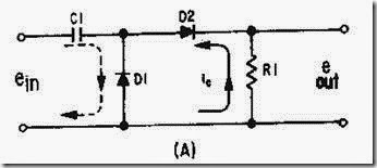
Figure 4-18, view (A), illustrates the circuit of a positive-diode clamper. Resistor R1 provides a discharge path for C1. This resistance is large in value so that the discharge time of C1 will be long compared to the input pulse width. The diode provides a fast charge path for C1. After C1 becomes charged it acts as a voltage source. The input wave shape shown in view (B) is a square wave and varies between +25 volts and -25 volts. Compare each portion of the input wave shape with the corresponding output wave shape. Keep Kirchhoff’s law in mind: The algebraic sum of the voltage drops around a closed loop is 0 at any instant.

clip_image019

Figure 4-18A.—Positive damper and waveform.

clip_image021

Figure 4-18B.—Positive damper and waveform.

At T0 the -25 volt input signal appears across R1 and D1 (the capacitor is a short at the first instant). The initial voltage across R1 and D1 causes a voltage spike in the output. Because the charge time of C1 through D1 is almost instantaneous, the duration of the pulse is so short that it has only a negligible effect on the output. The -25 volts across D1 makes the cathode negative with respect to the anode and the diode conducts heavily. C1 quickly charges through the small resistance of D1. As the voltage across C1 increases, the output voltage decreases at the same rate. The voltage across C1 reaches -25 volts and the output is at 0 volts.

At T1 the +25 volts already across the capacitor and the +25 volts from the input signal are in series and aid each other (SERIES AIDING). Thus, +50 volts appears across R1 and D1. At this time, the cathode of D1 is positive with respect to the anode, and the diode does not conduct. From T1 to T2, C1 discharges to approximately +23 volts (because of the large values of R and C) and the output voltage drops from +50 volts to +48 volts.

At T2 the input signal changes from +25 volts to -25 volts. The input is now SERIES OPPOSING with the +23 volts across C1. This leaves an output voltage of -2 volts (-25 plus +23 volts). The cathode of D1 is negative with respect to the anode and D1 conducts. From T2 to T3, C1 quickly charges through D1 from +23 volts to +25 volts; the output voltage changes from -2 volts to 0 volts.

At T3 the input signal and capacitor voltage are again series aiding. Thus, the output voltage felt across R1 and D1 is again +50 volts. During T3 and T4, C1 discharges 2 volts through R1. Notice that circuit operation from T3 to T4 is the same as it was from T1 to T2. The circuit operation for each square- wave cycle repeats the operation which occurred from T2 to T4.

Compare the input wave shape of figure 4-18, view (B), with the output wave shape. Note the following important points: (1) The peak-to-peak amplitude of the input wave shape has not been changed by the clamper circuit; (2) the shape of the output wave shape has not been significantly changed from that of the input by the action of the clamper circuit; and (3) the output wave shape is now all above 0 volts whereas the input wave shape is both above and below 0 volts. Thus, the lower part of the input wave shape has been clamped to a dc potential of 0 volts in the output. This circuit is referred to as a positive clamper since all of the output wave shape is above 0 volts and the bottom is clamped at 0 volts.

The positive clamper circuit is self-adjusting. This means that the bottom of the output waveform remains clamped at 0 volts during changes in input signal amplitude. Also, the output wave shape retains the form and peak-to-peak amplitude (50 volts in this case) of the input wave shape. When the input amplitude becomes greater, the charge of the capacitor becomes greater and the output amplitude becomes larger. When the input amplitude decreases, the capacitor does not charge as high as before and clamping occurs at a lower output voltage. The capacitor charge, therefore, changes with signal strength.

The size of R1 and C1 has a direct effect upon the operation of the clamper. Because of the small resistance of the diode, the capacitor charge time is short. If either R1 or C1 is made smaller, the capacitor discharges faster (TC = R · C).

The ability of a smaller value capacitor to quickly discharge to a lower voltage is an advantage when the amplitude of the input wave shape is suddenly reduced. However, for normal clamper operation, quick discharge time is a disadvantage. This is because one objective of clamping is to keep the output wave shape the same as the input wave shape. If the small capacitor allows a relatively large amount of the voltage to discharge with each cycle, then distortion occurs in the output wave shape. A larger portion of the wave shape then appears on the wrong side of the reference line.

Increasing the value of the resistor increases the discharge time (again, TC = R · C). This increased value causes the capacitor to discharge more slowly and produces an output wave shape which is a better reproduction of the input wave shape. A disadvantage of increasing the resistance value is that the larger resistance increases the discharge time of the capacitor and slows the self-adjustment rate of the circuit, particularly in case a sudden decrease in input amplitude should occur. The larger resistance has no effect on self-adjustment with a sudden rise in input amplitude. This is because the capacitor charges through the small resistance of the conducting diode.

Circuits often incorporate a compromise between a short RC time constant (for self-adjustment purposes) and a long RC time constant for less distortion. A point to observe is that the reverse resistance of the diode sometimes replaces the, physical resistor in the discharge path of the capacitor.

Positive-Diode Clamper With Bias

Biased clamping circuits operate in exactly the same manner as unbiased clampers, with one exception. That exception is the addition of a dc bias voltage in series with the diode and resistor. The size and polarity of this bias voltage determines the output clamping reference.

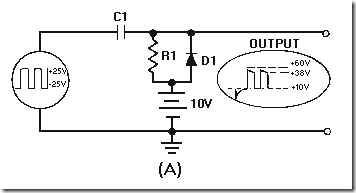
View (A) of figure 4-19 illustrates the circuit of a positive clamper with positive bias. It can be identified as a positive clamper because the cathode of the diode is connected to the capacitor. Positive bias can be observed by noting that the negative side of the battery is connected to ground. The purposes and actions of the capacitor, resistor, and diode are the same as in the unbiased clamper circuit just discussed.

clip_image022

Figure 4-19A.—Positive clamper with positive bias.

clip_image024

Figure 4-19B.—Positive clamper with positive bias.

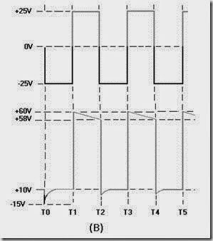
With no input, D1 is forward biased and the +10 V battery is the output. C1 will charge to +10 V and hold this charge until the first pulse is applied. The battery establishes the dc reference level at +10 volts. The input wave shape at the top of view (B) is a square wave which alternates between +25 and -25 volts. The output wave shape is shown at the bottom half of view (B).

Here, as with previous circuits, let’s apply Kirchhoff’s voltage law to determine circuit operation. With no input signal, the output is just the +10 volts supplied by the battery.

At time T0 the -25 volt signal applied to the circuit is instantly felt across R1 and D1. The -25 volt input signal forward biases D1, and C1 quickly charges to 35 volts. This leaves +10 volts across the output terminals for much of the period from T0 to T1. The polarity of the charged capacitor is, from the left to the right, minus to plus.

At T1 the 35 volts across the capacitor is series aiding with the +25 volt input signal. At this point (T1) the output voltage becomes +60 volts; the voltage across R1 and D1 is +50 volts, and the battery is

+10 volts. The cathode of D1 is positive with respect to the anode and the diode does not conduct. From T1 to T2, C1 discharges only slightly through the large resistance of R1. Assume that, because of the size of R1 and C1, the capacitor discharges just 2 volts (from +35 volts to +33 volts) during this period. Thus,

the output voltage drops from +60 volts to +58 volts.

At T2 the -25 volt input signal and the +33 volts across C1 are series opposing. This makes the voltage across the output terminals +8 volts. The cathode of the diode is 2 volts negative with respect to its anode and D1 conducts. Again, since the forward-biased diode is essentially a short, C1 quickly charges from +33 volts to +35 volts. During most of the time from T2 to T3, then, we find the output voltage is +10 volts.

At T3 the +25 volts of the input signal is series aiding with the +35 volts across C1. Again the output voltage is +60 volts. Observe that at T3 the conditions in the circuit are the same as they were at T1. Therefore, the circuit operation from T3 to T4 is the same as it was from T1 to T2. Circuit operation continues as a duplication of the operations which occurred from T1 to T3.

By comparing the input and output wave shapes, you should note the following: (1) The peak-to- peak amplitude of the input wave shape has not been changed in the output (for all practical purposes) by the action of the clamper circuit; (2) the shape of the input wave has not been changed; (3) the output wave shape is now clamped above +10 volts. Remember that this clamping level (+10 volts) is determined by the bias battery.

Positive-Diode Clamper With Negative Bias

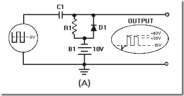
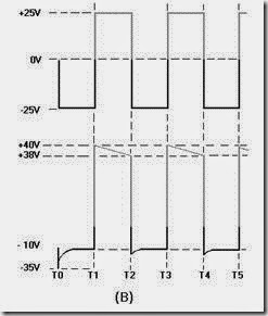
View (A) of figure 4-20 is a positive clamper with negative bias. Observe that with no input signal, the capacitor charges through R1 to the bias battery voltage; the output voltage equals -10 volts. The circuit has negative bias because the positive side of the battery is grounded. The output waveform is shown in view (B). Study the figure and waveforms carefully and note the following important points. Once again the peak-to-peak amplitude and shape of the output wave are, for all practical purposes, the same as the input wave. The lower extremity of the output wave is clamped to -10 volts, the value of the battery. Let’s look at the circuit operation. The capacitor is initially charged to -10 volts with no input signal, and diode D1 does not conduct.

clip_image025

Figure 4-20A.—Positive clamper with negative bias.

clip_image027

Figure 4-20B.—Positive clamper with negative bias.

The -25 volt input signal provides forward bias for D1. The capacitor charges to +15 volts and retains most of its charge because its discharge through R1 is negligible. The +25 volt input signal is series aiding the capacitor voltage and develops +40 volts between the output terminals. When the input voltage is -25 volts, D1 conducts and the output voltage is -10 volts (-25 volts plus +15 volts). In this way the output reference is clamped at -10 volts. Changing the size of the battery changes the clamping reference level to the new voltage.

NEGATIVE-DIODE CLAMPERS

Figure 4-21, view (A), illustrates the circuit of a negative-diode clamper. Compare this with the positive-diode clamper in view (A) of figure 4-18. Note that the diode is reversed with reference to ground. Like the positive clamper, resistor R1 provides a discharge path for C1; the resistance must be a large value for C1 to have a long discharge time. The low resistance of the diode provides a fast charge path for C1. Once C1 becomes charged, it acts as a source of voltage which will help determine the maximum and minimum voltage levels of the output wave shape. The input wave shape shown in view

(B) is a square wave which varies between +25 and -25 volts. The output wave shapes are shown in the bottom half of view (B). You will find that the operation of the negative clamper is similar to that of the positive clamper, except for the reversal of polarities.

clip_image029

Figure 4-21A.—Negative clamper and waveform.

clip_image031

Figure 4-21B.—Negative clamper and waveform.

At T0 the +25 volt input signal applied to the circuit appears across R1 and D1. This makes the anode of D1 positive with respect to the cathode and it conducts heavily. Diode resistance is very small causing C1 to charge quickly. As the voltage across C1 increases, the output voltage decreases. The voltage across C1 reaches 25 volts quickly; during most of T0 to T1, the output voltage is 0.

At T1 the voltage across the capacitor and the input voltage are series aiding and result in -50 volts appearing at the output. At this time the diode is reverse biased and does not conduct. Because of the size of R and C, the capacitor discharges only 2 volts to approximately 23 volts from T1 to T2. Using Kirchhoff’s voltage law to determine voltage in the circuit, we find that the output voltage decreases from -50 to -48 volts.

At T2 the +25 volt input signal and the 23 volts across C1 are series opposing. The output voltage is +2 volts. The anode of D1 is positive with respect to the cathode and D1 will conduct. From T2 to T3, C1 charges quickly from 23 to 25 volts through D1. At the same time, the output voltage falls from +2 to 0 volts.

At T3 the input and capacitor voltages are series aiding and the total output voltage is -50 volts. From T3 to T4, D1 is reverse biased and C discharges through R. The circuit operation is now the same as it was from T1 to T2. The circuit operation for the following square-wave cycles duplicates the operation which occurred from T1 to T3.

As was the case with the positive clamper, the amplitude and wave, shape of the output is almost identical to that of the input. However, note that the upper extremity of the output wave shape is clamped to 0 volts; that is, the output wave shape, for all practical purposes, lies entirely below the 0-volt reference level.

Negative-Diode Clamper With Negative Bias

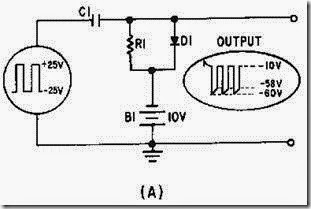
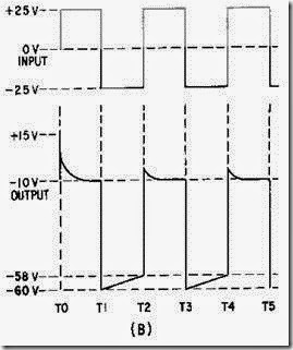
View (A) of figure 4-22 is the circuit of a negative clamper with negative bias. Again, with no input signal the capacitor charges to the battery voltage and the output is negative because the positive side of the battery is ground. The bottom of view (B) shows the output of the circuit. Study the figure carefully, and note the following important points. The peak-to-peak amplitude and shape of the output wave, for all practical purposes, are the same as that of the input wave. The output wave is clamped to -10 volts which is the value of the battery. Since this is a negative clamper, the upper extremity of the waveform touches the -10 volt reference line (and the rest of it lies below this voltage level).

clip_image033

Figure 4-22A.—Negative damper with negative bias.

clip_image035

Figure 4-22B.—Negative damper w ith negative bias.

Let’s review the important points of circuit operation. The capacitor is initially charged to -10 volts with no input signal. Applying Kirchhoff’s law we find that the +25 volt input signal and the 10-volt battery are series opposing. This series opposing forward biases D1 and the capacitor charges to -35 volts. The output voltage is equal to the sum of the capacitor voltage and the input voltage. Thus, the output voltage is -10 volts and the wave shape is clamped to -10 volts. With a -25 volt input, the charge maintained across C1 and the input are series aiding and provide a -60 volt output. C1 will discharge just before the next cycle begins and the input becomes positive. The +25 volt input signal and the approximately -23 volt charge remaining on C1 will forward bias D1 and the output will be clamped to the battery voltage. C1 will quickly charge to the input signal level. Thus, the output voltage varies between -10 and -60 volts and the wave shape is clamped to -10 volts.

Negative Clamper With Positive Bias

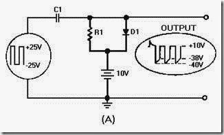
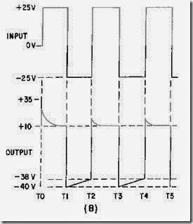
View (A) of figure 4-23 illustrates the circuit of a negative clamper with positive bias. With no input signal the capacitor charges to the battery voltage and the output is positive because the negative side of the battery is grounded. The output is illustrated in the bottom half of view (B). Study the figure carefully and note the following important points. The peak-to-peak amplitude and shape of the output waveform, for all practical purposes, are the same as that of the input. The output wave is clamped to +10 volts, the value of the battery. Since this is a negative clamper (cathode to ground), the top of the output wave touches the +10 volt reference line.

clip_image037

Figure 4-23A.—Negative clamper with positive bias.

clip_image039

Figure 4-23B.—Negative clamper with positive bias.

Let’s go over a summary of the circuit operation. With no input signal the capacitor charges to 10 volts. The +25 volt input signal forward biases D1. With the 10-volt battery and the input in series, the capacitor charges to -15 volts. The capacitor remains charged, for all practical purposes, since its discharge through R1 (very large) is almost negligible. The output voltage is equal to the algebraic sum of the capacitor voltage and the input voltage. The +25 volt input signal added to the -15 volt capacitor charge provides a +10 volt output. With a -25 volt input at T1, D1 is reverse-biased and the charge across C 1 adds to the input voltage to provide a -40 volt output. From T1 to T2, the capacitor loses only a small portion of its charge. At T2 the input signal is +25 volts and the input returns to +10 volts. The wave shape is negatively clamped to +10 volts by the battery.

We can say, then, that positive clamping sets the wave shape above (negative peak on) the reference level, and negative clamping places the wave shape below (positive peak on) the reference level.

Q6. What is the relative length of the time constant for the diode-capacitor combination in a damper (long or short)?

Q7. What is the relative length of the discharge time constant with respect to the charge time constant of a damper (long or short)?

Q8. A positive damper clamps which extremity of the output signal to 0 volts?

Q9. To which polarity does a positive damper with positive bins clamp the most negative extremity of the output waveform (positive or negative)?

Q10. What type damper (with bias) clamps the most negative extremity of the output waveform to a negative potential?

Q11. A negative damper damps which extremity of the output waveshape to 0 volts?

Q12. A negative damper with negative bias clamps the most positive extremity of the output wave shape to what polarity (positive or negative)?

Q13. What type of bias (positive or negative) is added to a negative damper for the most positive extremity of the wave shape to be clamped above 0 volts?

Q14. What would be the output of a negative clamper with a bias potential of 5 volts and an input voltage swing from +50 to 50 volts?


Wave shaping: common-base transistor clamper, shaping circuits and composition of nonsinusoidal waves.

COMMON-BASE TRANSISTOR CLAMPER

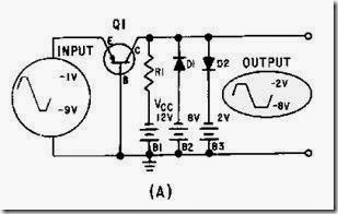
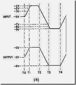
The common-base transistor clamper is similar to the dual diode limiter in figure 4-15, except for the addition of a transistor. In the previous clampers, we have clamped the output signal to a reference. In the transistor common-base clamper, we want to clamp the amplitude of the input to no more than nor less than certain values in the output. Also, we do not want phase inversion in the output. View (A) of figure 4-24 shows such a circuit. The transistor does not amplify the input and the output is not inverted. However, the two diode circuits serve to clamp the output between -2 volts and -8 volts, no matter what the varying input positive and negative extremes.

clip_image002

Figure 4-24A.—Common-base configuration clamper.

clip_image004

Figure 4-24B.—Common-base configuration clamper.

Look at view (B) as we continue. The input signal is a square-wave pulse type signal that varies in amplitude. Without an input signal, Q1 conducts and provides current through R1. This develops the output (collector to ground) potential which is assumed to be approximately -5 volts (VCC – ER1) for this discussion.

From T0 to T1 the output follows the input because of the increasing emitter-base forward bias. However, at T1 the collector voltage reaches -2 volts and D2 is forward biased. D2 conducts and limits the output to -2 volts (the value of B3). D2 conducts until T2 when the input decreases below -2 volts. At this time, D2 cuts off and the output again follows the input because of the decreasing forward bias on Q1. At T3 the input reaches -8 volts and forward biases D1. D1 conducts and any further increase (beyond -8 volts) of the input has no effect on the output. When the input returns to a value more positive than -8 volts, D1 cuts off and the output again follows the input. This circuit action is the same for all inputs. The output remains the same as the input except that both positive and negative extremes are clamped at -2 and -8 volts, respectively.

SHAPING CIRCUITS

Timing circuits and circuits which require a particular shape or "spike" of voltage, may use SHAPING circuits. Shaping circuits can be used to cause wave shapes, such as square waves, sawtooth waves, and trapezoidal waves, to change their shape. Shaping circuits may be either series RC or series RL circuits. The time constant is controlled in respect to the duration of the applied waveform. Notice that the wave shapes mentioned did not include the sine wave. These RC or RL shaping circuits do not change the shape of a pure sine wave.

The series RC and RL circuits electrically perform the mathematical operations of INTEGRATION and DIFFERENTIATION. Therefore, the circuits used to perform these operations are called INTEGRATORS and DIFFERENTIATORS. These names are applied to these circuits even though they do not always completely perform the operations of mathematical integration and differentiation.

COMPOSITION OF NONSINUSOIDAL WAVES

Pure sine waves are basic wave shapes from which other wave shapes can be constructed. Any waveform that is not a pure sine wave consists of two or more sine waves. Adding the correct frequencies at the proper phase and amplitude will form square waves, sawtooth waves, and other nonsinusoidal waveforms.

A waveform other than a sine wave is called a COMPLEX WAVE. You will see that a complex wave consists of a fundamental frequency plus one or more HARMONIC frequencies. The shape of a nonsinusoidal waveform is dependent upon the type of harmonics present as part of the waveform, their relative amplitudes, and their relative phase relationships. In general, the steeper the sides of a waveform, that is, the more rapid its rise and fall, the more harmonics it contains.

The sine wave which has the lowest frequency in the complex periodic wave is referred to as the FUNDAMENTAL FREQUENCY. The type and number of harmonics included in the waveform are dependent upon the shape of the waveform. Harmonics have two classifications — EVEN numbered and ODD numbered. Harmonics are always a whole number of times higher than the fundamental frequency and are designated by an integer (whole number). For example, the frequency twice as high as the fundamental frequency is the SECOND HARMONIC (or the first even harmonic).

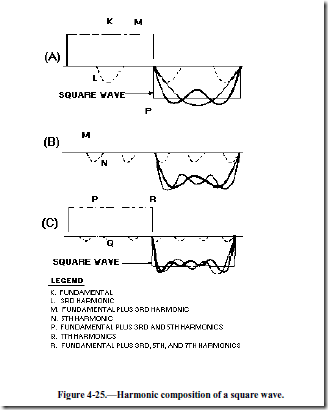
View (A) of figure 4-25 compares a square wave with sine waves. Sine wave K is the same frequency as the square wave (its fundamental frequency). If another sine wave (L) of smaller amplitude but three times the frequency (referred to as the third harmonic) is added to sine wave K, curve M is produced. The addition of these two waveforms is accomplished by adding the instantaneous values of both sine waves algebraically. Curve M is called the resultant. Notice that curve M begins to assume the shape of a square wave. Curve M is shown again in view (B).

image

As shown in view (B), when the fifth harmonic (curve N with its decreased amplitude) is added, the sides of the new resultant (curve P) are steeper than before. In view (C), the addition of the seventh harmonic (curve Q), which is of even smaller amplitude, makes the sides of the composite waveform (R) still steeper. The addition of more odd harmonics will bring the composite waveform nearer the shape of the perfect square wave. A perfect square wave is, therefore, composed of an infinite number of odd harmonics. In the composition of square waves, all the odd harmonics cross the reference line in phase with the fundamental.

A sawtooth wave, shown in figure 4-26, is made up of both even and odd harmonics. Notice that each higher harmonic is added in phase as it crosses the 0 reference in view (A), view (B), view (C), and view (D). The resultant, shown in view (D), closely resembles a sawtooth waveform.

clip_image007

Figure 4-26A.—Composition of a sawtooth wave.

clip_image009

Figure 4-26B.—Composition of a sawtooth wave.

clip_image011

Figure 4-26C.—Composition of a sawtooth wave.

clip_image013

Figure 4-26D.—Composition of a sawtooth wave.

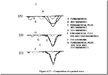
Figure 4-27 shows the composition of a peaked wave. Notice how the addition of each odd harmonic makes the peak of the resultant higher and the sides steeper. The phase relationship between the harmonics of the peaked wave is different from the phase relationship of the harmonics in the composition of the square wave. In the composition of the square wave, all the odd harmonics cross the

reference line in phase with the fundamental. In the peaked wave, harmonics such as the third, seventh, and so forth, cross the reference line 180 degrees out of phase with the fundamental; the fifth, ninth, and so forth, cross the reference line in phase with the fundamental.

image

Q15. What is the harmonic composition of a square wave? Q16. What is the peaked wave composed of?

Q17. What is the fundamental difference between the phase relationship of the harmonics of the square wave as compared to the harmonics of a peaked wave?


Wave shaping: limiters and series limiters.

WAVE SHAPING

LEARNING OBJECTIVES

Upon completion of this chapter you will be able to:

1. Explain the operation of series-limiter circuits.

2. Explain the operation of parallel-limiter circuits.

3. Describe the operation of a dual-diode limiter circuit.

4. Explain the operation of clamper circuits.

5. Explain the composition of nonsinusoidal waves.

6. Explain how RC and RL circuits are used as integrators.

7. Explain how RC and RL circuits are used as differentiators.

8. Explain the operation of a counting circuit.

9. Explain the operation of a step-by-step counter used as a frequency divider.

LIMITERS

As a technician, you will be confronted with many different types of LIMITING circuits. A LIMITER is defined as a device which limits some part of a waveform from exceeding a specified value. Limiting circuits are used primarily for wave shaping and circuit-protection applications.

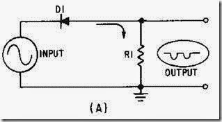
A limiter is little more than the half-wave rectifier you studied in NEETS, Module 6, Introduction to Electronic Emission, Tubes, and Power Supplies. By using a diode, a resistor, and sometimes a dc bias voltage, you can build a limiter that will eliminate the positive or negative alternations of an input waveform. Such a circuit can also limit a portion of the alternations to a specific voltage level. In this chapter you will be introduced to five types of limiters: SERIES-POSITIVE, SERIES-NEGATIVE, PARALLEL-POSITIVE, PARALLEL-NEGATIVE, and DUAL-DIODE LIMITERS. Both series- and

parallel-positive and negative limiters use biasing to obtain certain wave shapes. They will be discussed in this chapter.

The diode in these circuits is the voltage-limiting component. Its polarity and location, with respect to ground, are the factors that determine circuit action. In series limiters, the diode is in series with the output. In parallel limiters, the diode is in parallel with the output.

SERIES LIMITERS

You should remember, from NEETS, Module 7, Introduction to Solid-State Devices and Power Supplies, that a diode will conduct when the anode voltage is positive with respect to the cathode voltage. The diode will not conduct when the anode is negative in respect to the cathode. Keeping these two

simple facts in mind as you study limiters will help you understand their operation. Your knowledge of voltage divider action from NEETS, Module 1, Introduction to Matter, Energy, and Direct Current will also help you understand limiters.

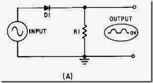
In a SERIES LIMITER, a diode is connected in series with the output, as shown in view (A) of figure 4-1. The input signal is applied across the diode and resistor and the output is taken across the resistor. The series-limiter circuit can limit either the positive or negative alternation, depending on the polarity of the diode connection with respect to ground. The circuit shown in figure 4-1, view (B), is a SERIES-POSITIVE LIMITER. Reversing D1 would change the circuit to a SERIES-NEGATIVE LIMITER.

clip_image002

Figure 4-1A.—Series-positive limiter.

clip_image004

Figure 4-1B.—Series-positive limiter.

Series-Positive Limiter

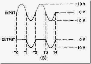
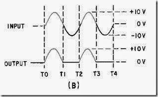
Let’s look at the series-positive limiter and its outputs in figure 4-1. Diode D1 is in series with the output and the output is taken across resistor R1. The input must be negative with respect to the anode of the diode to make the diode conduct. When the positive alternation of the input signal (T0 to T1) is applied to the circuit, the cathode is positive with respect to the anode. The diode is reverse biased and will not conduct. Since no current can flow, no output is developed across the resistor during the positive alternation of the input signal.

During the negative half cycle of the input signal (T1 to T2), the cathode is negative with respect to the anode. This causes D1 to be forward biased. Current flows through R1 and an output is developed.

The output during each negative alternation of the input is approximately the same as the input (-10 volts) because most of the voltage is developed across the resistor.

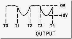
Ideally, the output wave shape should be exactly the same as the input wave shape with only the limited portion removed. When the diode is reverse biased, the circuit has a small amount of reverse current flow, as shown just above the 0-volt reference line in figure 4-2. During the limiting portion of the input signal, the diode resistance should be high compared to the resistor. During the time the diode is conducting, the resistance of the diode should be small as compared to that of the resistor. In other words, the diode should have a very high front-to-back ratio (forward resistance compared to reverse resistance). This relationship can be better understood if you study the effects that a front-to-back resistance ratio has on circuit output.

clip_image006

Figure 4-2.—Actual output of a series-positive limiter.

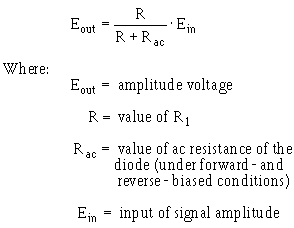
The following formula can be used to determine the output amplitude of the signal:

clip_image007

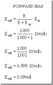
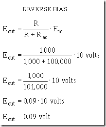
Let’s use the formula to compare the front-to-back ratio of the diode in the forward- and reverse- biased conditions.

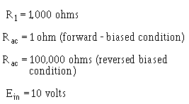
Given:

clip_image008

clip_image009

clip_image010

You can readily see that the formula comparison of the forward- and reverse-bias resistance conditions shows that a small amount of reverse current will flow during the limited portion of the input waveform. This small amount of reverse current will develop as the small positive voltage (0.09 volt) shown in figure 4-2 (T0 to T1 and T2 to T3). The actual amount of voltage developed will depend on the type of diode used. For the remainder of this chapter, we will use only idealized waveforms and disregard this small voltage.

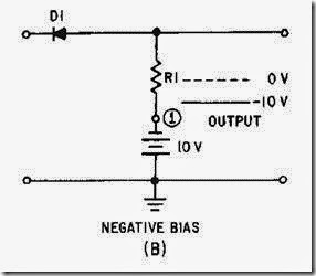
SERIES-POSITIVE LIMITER WITH BIAS.—In the series-positive limiter (figure 4-1, view (A)), the reference point at the bottom of resistor R1 is ground, or 0 volts. By placing a dc potential at point (1) in figure 4-3 (views (A) and (B)), you can change the reference point. The reference point changes by the amount of dc potential that is supplied by the battery. The battery can either aid or oppose the flow of current in the series-limiter circuit. POSITIVE BIAS (aiding) is shown in view (A) and NEGATIVE BIAS (opposing) is shown in view (B).

clip_image012

Figure 4-3A.—Positive and negative bias. POSITIVE BIAS.

clip_image014

Figure 4-3B.—Positive and negative bias. NEGATIVE BIAS.

When the dc aids forward bias, as in view (A), the diode conducts even with no signal applied. An input signal sufficiently positive to overcome the dc bias potential is required to reverse bias and cut off the diode.

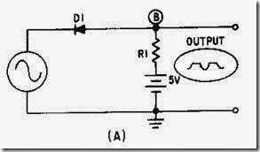
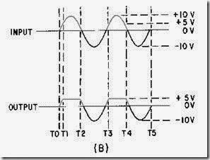
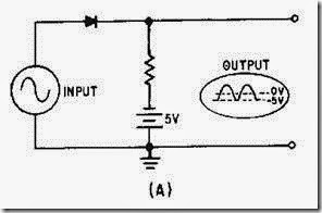
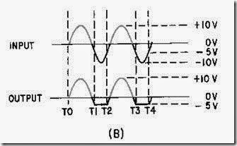
Let’s look at a series-positive limiter with positive bias as shown in figure 4-4, views (A) and (B). The diode will conduct until the input signal exceeds +5 at T1 on the positive alternation of the input signal. When the positive alternation exceeds +5 volts, the diode becomes reverse biased and limits the positive alternation of the output signal to +5 volts. This is because there is no current flow through resistor R1 and battery voltage is felt at point (B). The diode will remain reverse biased until the positive alternation of the input signal decreases to just under +5 volts at T2. At this time, the diode again becomes forward biased and conducts. The diode will remain forward biased from T2 to T3. During this period the negative alternation of the input is passed through the diode without being limited. From T3 to T4 the diode is again reverse biased and the output is again limited.

clip_image016

Figure 4-4A.—Series-positive limiter with positive bias.

clip_image018

Figure 4-4B.—Series-positive limiter with positive bias.

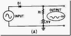
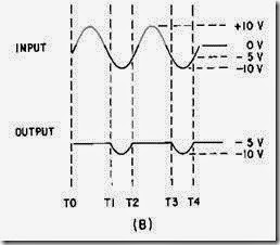
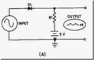
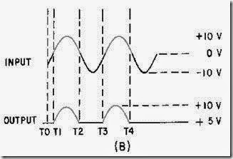
Now let’s look at what takes place when reverse bias is aided, as shown in figure 4-5, view (A). The diode is negatively biased with -5 volts from the battery. In view (B), compare the output to the input signal applied. From T0 to T1 the diode is reverse biased and limiting takes place. The output is at -5 volts (battery voltage) during this period. As the negative alternation increases toward -10 volts (T1), the cathode of the diode becomes more negative than the anode and is forward biased. From T1 to T2 the input signal is passed to the output. The diode remains forward biased until the negative alternation has decreased to -5 volts at T2. At T2 the cathode of the diode becomes more positive than the anode, and the diode is again reverse biased and remains so until T3.

clip_image020

Figure 4-5A.—Series-positive limiter with negative bias.

clip_image022

Figure 4-5B.—Series-positive limiter with negative bias.

Series-Negative Limiter

In view (A) of figure 4-6, the SERIES-NEGATIVE LIMITER limits the negative portion of the waveform, as shown in view (B). Let’s consider the input signal and determine how the output is produced. During T0 to T1 (view (B)), the anode is more positive than the cathode and the diode conducts. Current flows up through the resistor and the diode, and a positive voltage is developed at the output. The voltage across the resistor is essentially the same as the voltage applied to the circuit.

clip_image024

Figure 4-6A.—Series-negative limiter.

clip_image026

Figure 4-6B.—Series-negative limiter.

During T1 to T2 the anode is negative with respect to the cathode and the diode does not conduct. This portion of the output is limited because no current flows through the resistor.

As you can see, the only difference between series-positive and series-negative limiters is that the diode is reversed in the negative limiters.

SERIES-NEGATIVE LIMITER WITH BIAS.—View (A) of figure 4-7 shows a series-negative limiter with negative bias. The diode is forward biased and conducts with no input signal. In view (B) it will continue to conduct as the input signal swings first positive and then negative (but only to -5 volts) from T0 through T1. At T1 the input becomes negative with respect to the -5 volt battery bias. The diode becomes reverse biased and is cutoff until T2 when the anode again becomes positive with respect to the battery voltage (-5 volts) on the cathode. No voltage is developed in the output by R1 (no current flow) and the output is held at -5 volts from T1 to T2. With negative bias applied to a series-negative limiter, only a portion of the negative signal is limited.

clip_image028

Figure 4-7A.—Series-negative limiter with negative bias.

clip_image030

Figure 4-7B.—Series-negative limiter with negative bias.

Now let’s look at a series-negative limiter with positive bias, as shown in figure 4-8, view (A). Here we will remove all of the negative alternation and part of the positive alternation of the input signal. We have given a full explanation of the series-positive limiter, series-positive limiter with bias, series- negative limiter, and series-negative limiter with negative bias; therefore, you should have little difficulty understanding what is happening in the circuit in the figure.

clip_image032

Figure 4-8A.—Series-negative limiter with positive bins.

clip_image034

Figure 4-8B.—Series-negative limiter with positive bins.

The series-negative limiter with positive bias is different in only one aspect from the series-positive limiter with bias (figure 4-5) discussed earlier. The difference is that the diode is reversed and the output is of the opposite polarity.

Q1. Which portion of a sine-wave input is retained in the output of a series-positive limiter? Q2. Which portion of a sine-wave input is retained in the output of a series-negative limiter?

Q3. How can a series-positive limiter be modified to limit unwanted negative portions of the input signal?


Waveforms and wave generators: time-base generators.

TIME-BASE GENERATORS

Radar sets, oscilloscopes, and computer circuits all use sawtooth (voltage or current) waveforms. A sawtooth waveshape must have a linear rise. The sawtooth waveform is often used to produce a uniform, progressive movement of an electron beam across the face of an electrostatic cathode ray tube. This movement of the electron beam is known as a SWEEP. The voltage which causes this movement is known as SWEEP VOLTAGE and the circuit which produces this voltage is the SWEEP GENERATOR, or TIME-BASE GENERATOR. Most common types of time-base generators develop the sawtooth waveform by using some type of switching action with either the charge or discharge of an RC or RL circuit.

Sawtooth Wave

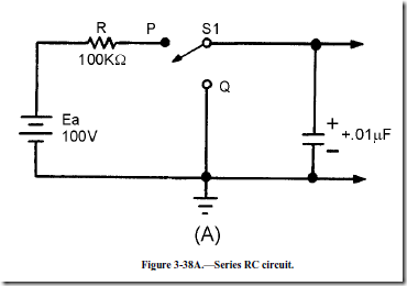
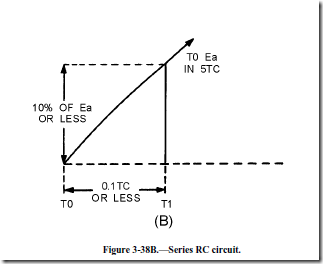
A sawtooth wave can be generated by using an RC network. Possibly the simplest sawtooth generator is that which is shown in figure 3-38, view (A). Assume that at T0 (view (B)), S1 is placed in position P. At the instant the switch closes, the applied voltage (Ea) appears at R. C begins to charge to E a through R. If S1 remains closed long enough, C will fully charge to Ea. You should remember from NEETS, Module 2, Alternating Current and Transformers, that a capacitor takes 5 time constants (5TC) to fully charge. As the capacitor charges to the applied voltage, the rate of charge follows an exponential curve. If a linear voltage is desired, the full charge time of the capacitor cannot be used because the exponential curve becomes nonlinear during the first time constant.
image

image

However, during the first 10 percent of the first time constant, the rate of voltage change across the capacitor is almost constant (linear). Suppose that S1 is placed in position P at T0, and C is allowed to charge for 0.1 time constant. This is shown as T0 to T1 in view (B). Notice that the rate of voltage change across C is nearly constant between T0 and T1. Now, assume that at T1 the switch is moved from position P to position Q. This shorts the capacitor, and it discharges very rapidly. If the switch is placed back in position P, the capacitor will start charging again.

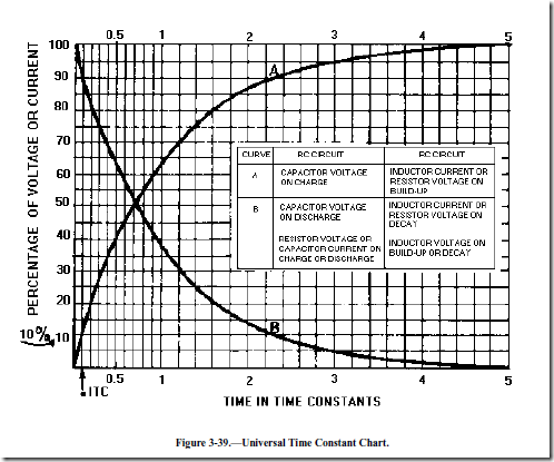
By selecting the sizes of R and C, you can have a time constant of any value you desire. Further, by controlling the time S1 remains closed, you can generate a sawtooth of any duration. Figure 3-39 is the Universal Time Constant Chart. Notice in the chart that if 1 time constant is 1,000 microseconds, S1 (figure 3-38, view (A )) can be closed no longer than 100 microseconds to obtain a reasonable linear sawtooth. In this example, C1 will charge to nearly 10 volts in 0.1 time constant.
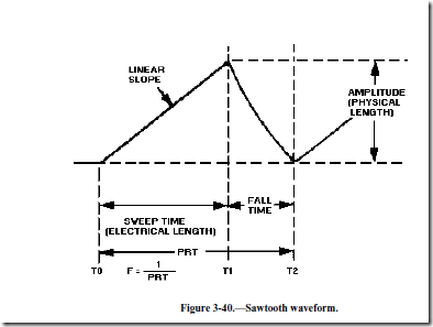
imageThe dimensions of the sawtooth waveform used in oscilloscopes need to be discussed before going any further. Figure 3-40 shows a sawtooth waveform with the various dimensions labeled. The duration of the rise of voltage (T0 to T1) is known as the SWEEP TIME or ELECTRICAL LENGTH. The electron beam of an oscilloscope moves across the face of the cathode ray tube during this sweep time. The amount of voltage rise per unit of time is referred to as the SLOPE of the waveform. The time from T1 to T2 is the capacitor discharge time and is known as FALL TIME or FLYBACK TIME. This discharge time is known as flyback time because during this period the electron beam returns, or "flys" back, from the end of a scanning line to begin the next line.
image

The amplitude of the rise of voltage is known as the PHYSICAL LENGTH. It is called physical length because the greater the peak voltage, the greater physical distance the beam will move. For example, the amount of voltage needed to move an electron beam 4 inches is twice the amount needed to move the beam 2 inches across the face of a given crt.

The voltage rise between T0 to T1 is the LINEAR SLOPE of the wave. The linearity of the rise of voltage is determined by the amount of time the capacitor is allowed to charge. If the charge time is kept short (10 percent or less of 1TC), the linearity is reasonably good.

As stated in the discussion of time-base generators, the waveform produced from any sawtooth generator must be linear. A LINEAR SAWTOOTH is one that has an equal change in voltage for an equal change in time. Referring to the Universal Time Constant Chart in figure 3-39, you can see that the most desirable part of the charge curve is the first one-tenth (0.1) of the first TC.

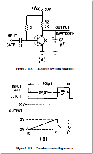
Figure 3-41, view (A), is a transistor sawtooth generator. In this figure R1 is a forward-biasing resistor for Q1, C1 is a coupling capacitor, and Q1 is serving as a switch for the RC network consisting of R2 and C2. With forward bias applied to Q1, the generator conducts at saturation, and its collector voltage (the output) is near 0 volts as indicated by the waveform in view (B). The charge felt by C1 is nearly 0. A negative gate is applied to the base of Q1 to cut off Q1 and allow C2 to charge. The length of time that the gate is negative determines how long Q1 will remain cut off and, in turn, how long C2 will be allowed to charge. The length of time that C2 is allowed to charge is referred to as the electrical length of the sawtooth that is produced.
image

The amplitude of the sawtooth that is produced is limited by the value of VCC that is used in the circuit. For example, if the voltage is 30 volts, and the capacitor (C2) is allowed to charge to 10 percent of 30 volts, then the amplitude of the sawtooth will be 3 volts (see figure 3-41, view (B)). If VCC is increased to 40 volts, C2 will charge to 10 percent of 40 volts and the output will increase in amplitude to 4 volts. Changing the value of V CC in the circuit changes the amplitude of the sawtooth waveform that is produced; amplitude determines the physical length. Since the number of time constants used in the circuit has not been changed, linearity does not change with a change in VCC.

The linear slope that is produced by the circuit is dependent on two variables; (1) the time constant of the RC circuit and (2) the gate length of the gate applied to the circuit. The circuit will produce a linear sawtooth waveshape if the components selected are such that only one-tenth of 1 TC or less is used. The GATE LENGTH is the amount of time that the gate is applied to the circuit and controls the time that the capacitor is allowed to charge. The value of R2 and C2 determines the time for 1 time constant (TC = RC). To determine the number of time constants (or the fraction of 1TC) used, divide the time for 1 time constant into the time that the capacitor is allowed to charge:

clip_image012

In figure 3-41, view (B), gate length is 500 microseconds and TC is the product of R2 (5 kilohms) and C2 (1 microfarad). The number of time constants is computed as follows:
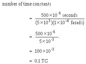
clip_image013

Therefore, 0.1TC is the length of time required to produce a linear rise in the sawtooth waveform.

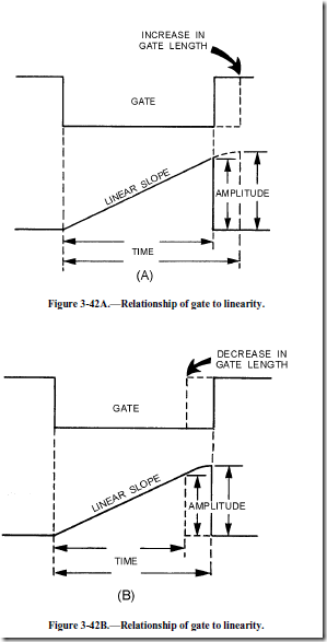
clip_image014

shows that an increase in gate length increases the number of time constants. An increase in the number of time constants decreases linearity. The reason is that C2 now charges to a greater percentage of the applied voltage, and a portion of the charge curve is being used that is less linear. The waveform in figure 3-42, view (A), shows an increase in amplitude (physical length), an increase in the time that C2 is allowed to charge (electrical length), and a decrease in linearity. If a smaller percentage of VCC is used, the gate length is decreased. As shown in view (B), this decreased gate length results in an increase in linearity, a decrease in the time that C2 is allowed to charge (electrical length), and a decrease in amplitude (physical length).
image

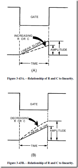
Changing the value of R and C in the circuit affects linearity since they control the time for 1 time constant. For example, if the value of C2 is increased in the circuit, as shown in figure 3-43, view (A), the time for 1 time constant increases and the number of time constants then decreases. With a decrease in the number of time constants, linearity increases. The reason is that a smaller percentage of VCC is used, and the circuit is operating in a more linear portion of the charge curve. Increasing the value of the TC (C2 or R2) decreases the amplitude of the sawtooth (physical length) because C2 now charges to a smaller percentage VCC for a given time. The electrical length remains the same because the length of time that C2 is allowed to charge has not been changed.
image

Decreasing the value of the TC (R2 or C2), as shown in figure 3-43, view (B), results in an increase in the number of time constants and therefore causes linearity to decrease. Anytime the number of time constants increases, the percentage of charge increases (see the Universal Time Constant Chart, figure 3- 39), and amplitude (physical length) increases. Without an increase in gate length, the time that C2 is allowed to charge through R2 remains the same; therefore, electrical length remains the same. Linearity is affected by gate length, the value of R, and the value of C; but is not affected by changing the value of VCC. Increasing the gate length decreases linearity, and decreasing gate length increases linearity. Increasing R or C in the circuit increases linearity, and decreasing R or C in the circuit decreases linearity.

The entire time of the sawtooth, from the time at which the capacitor begins charging (T0 in figure 3-41, view (B)) to the time when it starts charging again (T2), is known as the prt of the wave. The pulse repetition frequency of the sawtooth wave is:

clip_image023

UNIJUNCTION SAWTOOTH GENERATOR.—So far, you have learned in this chapter that a switch and an RC network can generate a sawtooth waveform. When using a unijunction transistor as the switch, a simple sawtooth generator looks like the circuit in figure 3-44, view (A); the output waveshapes are shown in view (B). You may want to review unijunction transistors in NEETS, Module 7, Introduction to Solid-State Devices and Power Supplies, chapter 3, before continuing.

clip_image025

Figure 3-44A.—Unijunction sawtooth generator. SCHEMATIC.

When the 20 volts is applied across B2 and B1, the n-type bar acts as a voltage- divider. A voltage of 12.8 volts appears at a point near the emitter. At the first instant, C1 has no voltage across it, so the output of the circuit, which is taken across the capacitor (C1), is equal to 0 volts. (The voltage across C1 is also the voltage that is applied to the emitter of the unijunction.) The unijunction is now reverse biased. After T0, C1 begins to charge toward 20 volts.

At T1, the voltage across the capacitor (the voltage on the emitter) has reached approximately 12.8 volts. This is the peak point for the unijunction, and it now becomes forward biased. With the emitter forward biased, the impedance between the emitter and B1 is just a few ohms. This is similar to placing a short across the capacitor. The capacitor discharges very rapidly through the low resistance of B1 to E.

As C1 discharges, the voltage from the emitter to B1 also decreases. Q1 will continue to be forward biased as long as the voltage across C1 is larger than the valley point of the unijunction.

At T2 the 3-volt valley point of the unijunction has been reached. The emitter now becomes reverse biased and the impedance from the emitter to B1 returns to a high value. Immediately after T2, Q1 is reverse biased and the capacitor has a charge of approximately 3 volts. C1 now starts to charge toward 20 volts as it did originally (just after T0). This is shown from T2 to T3 in figure 3-44, view (B).

clip_image027

Figure 3-44B.—Unijunction sawtooth generator. EMITTER WAVEFORM.

The circuit operation from now on is just a continuous repetition of the actions between T2 and T4. The capacitor charges until the emitter becomes forward biased, the unijunction conducts and C1 discharges, and Q1 becomes reverse biased and C1 again starts charging.

Now, let’s determine the linearity, electrical length, and amplitude of the output waveform. First, the linearity: To charge the circuit to the full 20 volts will take 5 time constants. In the circuit shown in figure 3-44, view (B), C1 is allowed to charge from T2 to T3. To find the percentage of charge, use the equation:
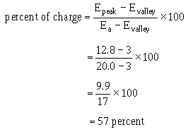
clip_image028

This works out to be about 57 percent and is far beyond the 10 percent required for a linear sweep voltage. The linearity is very poor in this example.

The electrical length (sweep time), which is measured from T2 to T3, can be found by multiplying RC times the number of time constants. Refer to the Universal Time Constant Chart (figure 3-39) again to find that 57 percent is 0.83TC. By multiplying 0.83 times R1C1, you will find that the electrical length is approximately 21 milliseconds:
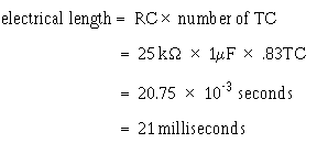
clip_image029

The physical length (amplitude) is determined by subtracting the valley point from the peak point. This is 9.8 volts in the example (12.8 volts – 3 volts).

For a sweep generator that produces a more linear output sawtooth waveform, refer to the circuit in figure 3-45, view (A). R1 and C1 form the RC time constant. Notice that the capacitor charges toward 35 volts (VE) in this circuit.

clip_image031

Figure 3-45A.—Improved unijunction sawtooth generator.

clip_image033

Figure 3-45B.—Improved unijunction sawtooth generator.

The output waveform is shown in figure 3-45, view (B). With a lower voltage applied from B1 to B2, the peak and valley points are closer together. Calculating the percentage of charge:
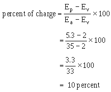
clip_image034

The linearity in this case is good. Using the Universal Time Constant Chart, a 10-percent charge amounts to 0.1 time constant. The electrical length is, again, RC times the number of time constants. With R1 at 300 kilohms and C1 at .005 microfarads, the time constant is 1,500 microseconds. One-tenth of a time constant is equal to 150 microseconds; so the electrical length is 150 microseconds. Prt is the electrical length plus the fall or flyback time. If C1 discharges from 5.3 volts to 2 volts in 15 microseconds, then the prt is 150 + 15, or 165 microseconds. The prf is about 6 kilohertz

clip_image035

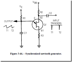
Some unijunction circuits are triggered to obtain a very stable prf. One method is to apply triggers to B2, as shown in figure 3-46. Negative triggers applied to B2 reduce the inter-base voltage enough to cause a forward bias condition in the emitter circuit. This cuts off the sweep and allows C1 to discharge through the B1-to-emitter circuit. Then, C1 recharges until the next trigger arrives and C1 discharges. Circuit operation and parameters are figured in the same manner as in the previous sawtooth circuits.
image

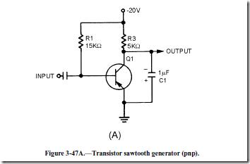
TRANSISTOR SAWTOOTH GENERATOR.—The next sawtooth generator uses a conventional pnp transistor, as shown in figure 3-47, view (A). This generator also uses an RC network, and the transistor provides the switching action.
image

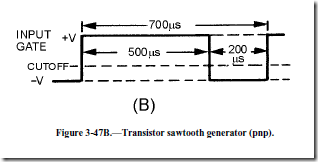
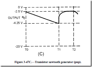
The waveforms for the circuit are shown in views (B) and (C). With no input signals, Q1 is biased near saturation by R1. The voltage across C1 is very low (-2.5 volts) because load resistor R3 drops most of the applied voltage. The transistor must be cut off to allow C1 to charge. To cut off Q1, a positive rectangular wave is used.
image

image

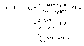
Since Q1 is a pnp transistor, a positive voltage must be used to drive it to cutoff. Figure 3-47, view (B), shows a rectangular wave input 500 microseconds long on the positive alternation. At T0, the positive gate applied to the base of Q1 cuts off Q1. This effectively removes the transistor from the circuit (opens the switch), and C1 charges through R3 toward 20 volts. Starting with a charge of -2.5 volts at T0, C1 charges (T0 to T1) for 500 microseconds to -4.25 volts at T1. Let’s determine the percent of charge:
clip_image044

This allows nearly a linear rise of voltage across C1.

Increasing the value of R3 or C1 increases the time constant. The capacitor will not charge to as high a voltage in the same period of time. Decreasing the width of the gate and maintaining the same time constant also prevents the capacitor from charging as much. With less charge on the capacitor, and the same voltage applied, linearity has been improved. Decreasing R3 or C1 or increasing gate width decreases linearity. Changing the applied voltage will change the charge on the capacitor. The percentage of charge remains constant; however, it does not affect linearity.

At T1, the positive alternation of the input gate ends, and Q1 returns to a forward-bias condition. A transistor that is near saturation has very low resistance, so C1 discharges rapidly between T1 and T2, as shown in figure 3-47, view (C). The capacitor discharges in less than 200 microseconds, the length of the negative alternation of the gate. The negative gate is made longer than the discharge time of the capacitor to ensure that the circuit has returned to its original condition.

From T1 to T2, the capacitor discharges and the circuit returns to its original condition, ready for another positive gate to arrive. The next positive gate arrives at T2 and the actions repeats.

The amplitude of the output sawtooth wave is equal to 1.75 volts (4.25 volts minus 2.5 volts). The electrical length is the same as the positive alternation of the input gate, or 500 microseconds. The prt is 700 microseconds (500 + 200) and the prf is 1/prt or 1,428 hertz.

Trapezoidal Sweep Generator

Normally, oscilloscopes and synchroscopes use ELECTROSTATIC DEFLECTION and, as the name implies, electrostatic fields move the electron beam. The need here is for a sawtooth voltage waveform.

Another method of electron beam deflection is ELECTROMAGNETIC DEFLECTION. Currents through a coil produce electromagnetic fields which position the beam of electrons. The electromagnetic system requires a sawtooth of current which increases at a linear rate. Because of the inherent characteristics of a coil, a sawtooth voltage does not cause a linear increase of current. A linear increase of current requires a TRAPEZOIDAL voltage waveform applied to a coil. This section discusses the generation of a trapezoidal wave.

Figure 3-48 shows a trapezoidal wave. The wave consists of a sharp, almost instantaneous jump in voltage followed by a linear rise to some peak value. The initial change in voltage at T0 is called a JUMP or STEP. The jump is followed by a linear sawtooth voltage rise. The time from the jump to the peak amplitude is the sum of the jump voltage and the sawtooth peak; where the peak value occurs is the electrical length. The peak voltage amplitude is the sum of the jump voltage and the sawtooth peak voltage. The waveshape can be considered a combination of a rectangular wave and a sawtooth wave.
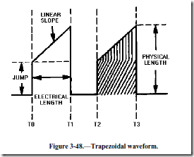
imageThe inductance and resistance of a coil form a series RL circuit. The voltage drop across this inductance and resistance must be added to obtain the voltage waveform required to produce a linear rise in current. A linear rise of current produces a linear rise of voltage across the resistance of the coil and a constant voltage drop across the inductance of the coil.

Assume figure 3-49, view (A), represents deflection coils. If we apply a voltage waveshape to the circuit, which will provide a square wave across inductor L, and a sawtooth across resistor R, then a linear current rise will result.

clip_image048

Figure 3-49A.—Series LR circuit.

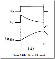
View (B) of figure 3-49 shows the waveforms when Ea is a square wave. Recall that the inductor acts as an open circuit at this first instant. Current now starts to flow and develops a voltage across the resistor. With a square wave applied, the voltage across the inductor starts to drop as soon as any voltage appears across the resistor. This is due to the fact that the voltage across the inductor and resistor must add up to the applied voltage.
image

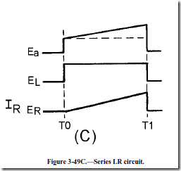
With Ea being a trapezoidal voltage, as shown in figure 3-49, view (C), the instant current flows, a voltage appears across the resistor, and the applied voltage increases. With an increasing applied voltage, the inductor voltage remains constant (EL) at the jump level and circuit current (I R) rises at a linear rate from the jump voltage point. Notice that if you add the inductor voltage (EL) and resistor voltage (ER) at any point between times T0 and T1, the sum is the applied voltage (Ea). The key fact here is that a trapezoidal voltage must be applied to a sweep coil to cause a linear rise of current. The linear rise of current will cause a uniform, changing magnetic field which, in turn, will cause an electron beam to move at a constant rate across a crt.
image

There are many ways to generate a trapezoidal waveshape. For example, the rectangular part could be generated in one circuit, the sawtooth portion in another, and the two combined waveforms in still a third circuit. A far easier, and less complex, way is to use an RC circuit in combination with a transistor to generate the trapezoidal waveshape in one stage.

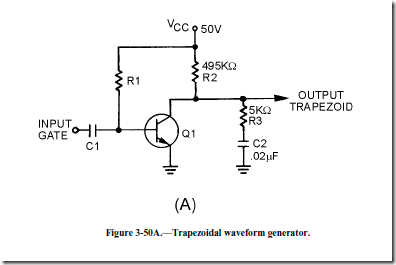
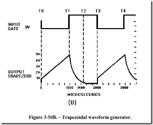
Figure 3-50, view (A), shows the schematic diagram of a trapezoidal generator. The waveshapes for the circuit are shown in view (B). R1 provides forward bias for Q1 and, without an input gate, Q1 conducts very hard (near saturation), C1 couples the input gate signal to the base of Q1. R2, R3, and C2 form the RC network which forms the trapezoidal wave. The output is taken across R3 and C2.
image


image

With Q1 conducting very hard, collector voltage is near 0 volts prior to the gate being applied. The voltage across R2 is about 50 volts. This means no current flows across R3, and C2 has no charge.

At T0, the negative alternation of the input gate is applied to the base of Q1, driving it into cutoff. At this time the transistor is effectively removed from the circuit. The circuit is now a series-RC network with 50 volts applied. At the instant Q1 cuts off, 50 volts will appear across the combination of R2 and R3 (the capacitor being a short at the first instant). The 50 volts will divide proportionally, according to the size of the two resistors. R2 then will have 49.5 volts and R3 will have 0.5 volt. The 0.5 volt across R3 (jump resistor) is the amplitude of the jump voltage. Since the output is taken across R3 and C2 in series, the output "jumps" to 0.5 volt.

Observe how a trapezoidal generator differs from a sawtooth generator. If the output were taken across the capacitor alone, the output voltage would be 0 at the first instant. But splitting the R of the RC network so that the output is taken across the capacitor and part of the total resistance produces the jump voltage.

Refer again to figure 3-50, view (A) and view (B). From T0 to T1, C2 begins charging toward 50 volts through R2 and R3. The time constant for this circuit is 10 milliseconds. If the input gate is 1,000 microseconds, the capacitor can charge for only 10 percent of 1TC, and the sawtooth part of the trapezoidal wave will be linear.

At T1, the input gate ends and Q1 begins to conduct heavily. C2 discharges through R3 and Q1. The time required to discharge C2 is primarily determined by the values of R3 and C2. The minimum discharge time (in this circuit) is 500 microseconds (5KW ´ .02µF ´ 5). At T2, the capacitor has discharged back to 0 volts and the circuit is quiescent. It remains in this condition until T3 when another gate is applied to the transistor.

The amplitude of the jump voltage was calculated to be 0.5 volt. The sawtooth portion of the wave is linear because the time, T0 to T1, is only 10 percent of the total charge time. The amplitude of the trapezoidal wave is approximately 5 volts. The electrical length is the same as the input gate length, or 1,000 microseconds. Linearity is affected in the same manner as in the sawtooth generator. Increasing R2 or C2, or decreasing gate width, will improve linearity. Changing the applied voltage will increase output amplitude, but will not affect linearity.

Linearity of the trapezoidal waveform, produced by the circuit in figure 3-50, view (A) and view (B) depends on two factors, gate length and the time constant of the RC circuit. Recall that these are the same factors that controlled linearity in the sawtooth generator. The formula developed earlier still remains true and enables us to determine what effect these factors have on linearity.

clip_image057

An increase in gate length results in an increase in the number of time constants and an increase in the percentage of charge that the capacitor will take on during this time interval. As stated earlier, if the number of time constants were to exceed 0.1, linearity would decrease. The reason for a decrease in linearity is that a greater percentage of VCC is used. The Universal Time Constant Chart (figure 3-39) shows that the charge line begins to curve. A decrease in gate length has the opposite effect on linearity in that it causes linearity to increase. The reason for this increase is that a smaller number of time constants are used and, in turn, a smaller percentage of the applied VCC is used.

Changing the value of resistance or capacitance in the circuit also affects linearity. If the value of C2 or R3 is increased, the time is increased for 1 time constant. An increase in the time for 1TC results in a decrease in the number of time constants required for good linearity. As stated earlier, a decrease in the number of time constants results in an increase in linearity (less than 0.1TC). In addition to an increase in jump voltage (larger value of R3) and a decrease in the amplitude (physical length) of the sawtooth produced by the circuit, electrical length remains the same because the length of the gate was not changed.

R2 has a similar effect on linearity because it is in series with R3. As an example, decreasing the value of R2 results in a decrease in linearity. The equation

clip_image057[1]

illustrates that by decreasing R (TC = RC), TC decreases and an increase in the number of time constants causes a decrease in linearity. Other effects are an increase in jump voltage and an increase in the amplitude (physical length) of the sawtooth.

Changing the value of VCC does not affect linearity. Linearity is dependent on gate length, R, and C. VCC does affect the amplitude of the waveform and the value of jump voltage that is obtained.

Q11. For an RC circuit to produce a linear output across the capacitor, the voltage across the capacitor may not exceed what percent of the applied voltage?

Q12. Increasing gate length in a sawtooth generator does what to linearity?

Q13. In a sawtooth generator, why is the transistor turned on for a longer time than the discharge time of the RC network?

Q14. What is added to a sawtooth generator to produce a trapezoidal wave?


Answers to questions and summary of waveforms and wave generators.

SUMMARY

This chapter has presented information on waveforms and wave generators. The information that follows summarizes the important points of this chapter.

A waveform which undergoes a pattern of changes, returns to its original pattern, and repeats that same pattern of changes is called a PERIODIC waveform.

Each completed pattern of a waveform is called a CYCLE.

clip_image002

A SQUARE WAVE is identified by, two alternations equal in time that are square in appearance. One alternation is called a PULSE. The time for one complete cycle is called the PULSE REPETITION TIME (prt). The number of times in one second that the cycle repeats itself is called PULSE REPETITION RATE (prr) or PULSE REPETITION FREQUENCY (prf). The length of the pulse measured in the figure (T0 to T1) is referred to as the PULSE WIDTH (pw). The left side of the pulse is referred to as the LEADING EDGE and the right side as the TRAILING EDGE.

clip_image004

A RECTANGULAR WAVE has two alternations that are unequal in time.

clip_image006

A SAWTOOTH WAVE has a linear increase in voltage followed by a rapid decrease of voltage at the end of the waveform.

clip_image008

A TRAPEZOIDAL WAVE looks like a sawtooth wave sitting on top of a square wave. The leading edge is called the JUMP voltage.

clip_image010

A TRIGGER is a very narrow pulse used to turn on or off another circuit.

clip_image012

A MULTIVIBRATOR is used to generate a square or rectangular wave. A multivibrator is basically two amplifiers with regenerative feedback.

The ASTABLE MULTIVIBRATOR has no stable state. The transistors alternately switch from cutoff to saturation at a frequency determined by the RC time constants of the coupling circuits.

clip_image014

The MONOSTABLE MULTIVIBRATOR has one stable state. One transistor conducts while the other is cut off. An external trigger must be applied to change this condition.

clip_image016

The BISTABLE MULTIVIBRATOR has two steady states. It remains in one of the stable states until a trigger is applied. It then switches to the other stable state until another trigger is applied.

clip_image018

The bistable multivibrator is also known as a FLIP-FLOP. The two inputs are SET and CLEAR. The two outputs are "1" and "0." A trigger pulse on the set input will cause the "1" output (negative or positive voltage depending on the type transistor used). At the same time the "0" output will equal 0 volts. This is the SET state.

clip_image020

A CLEAR STATE of a flip-flop exists when the "1" output measures low voltage (or 0 volts) and the "0" output is high voltage. The flip-flop will flop to the CLEAR state only upon application of a trigger pulse to the CLEAR (C) input.

clip_image022

There is a third lead on some flip-flops. This lead is the TOGGLE (T) input. Every time a trigger pulse is applied to the (T) input, the flip-flop will change states.

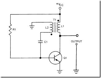
BLOCKING OSCILLATORS are used in applications which require a narrow pulse with sharp leading and trailing edges. They are used as TRIGGER GENERATORS or FREQUENCY DIVIDERS.

image

A SAWTOOTH GENERATOR voltage waveform has a linear change in voltage and a fast recovery time. The linear change in voltage is generated by taking the output from a capacitor. The sawtooth voltage waveform is used to provide electrostatic deflection in oscilloscopes.

clip_image026

A TRAPEZOIDAL GENERATOR voltage waveform is used to provide, a linear increase in current through a coil. A trapezoidal wave begins with a step or jump voltage, then a sawtooth wave. A trapezoidal wave of voltage is used in electromagnetic deflection display devices.

clip_image028

ANSWERS TO QUESTIONS Q1. THROUGH Q14.

A1. Multivibrator.

A2. Astable.

A3. Monostable.

A4. Bistable.

A5. RC coupling networks.

A6. One-shot.

A7. Two.

A8. Two.

A9. SET state. A10. Transformer.

A11. Ten percent.

A12. Decreases linearity.

A13. To allow the capacitor time to discharge. A14. A resistor.