Miniature/Micro miniature (2m) Repair Program and High-Reliability Soldering: Test Equipment and Repair Stations.

TEST EQUIPMENT

Microelectronic developments have had a great impact on the test equipment, tools, and facilities necessary to maintain systems using this technology. This section discusses, in general terms, the importance of these developments.

Early electronic systems could be completely checked-out with general-purpose electronic test equipment (GPETE), such as multimeters, oscilloscopes, and signal generators. Using this equipment to individually test the microelectronics components in one of today’s very complex electronic systems would be extremely difficult if not impossible. Therefore, improvements in system testing procedures have been necessary.

One such improvement in system testing is the design of a method that can test systems at various functional levels. This allows groups of components to be tested as a whole and reduces the time required to test components individually. One advantage of this method is that complete test plans can be written to provide the best sequencing of tests for wave shape or voltage outputs for each functional level. This method of testing has led to the development of special test sets, called AUTOMATED TEST EQUIPMENT (ATE). These test sets are capable of simulating actual operating conditions of the system being tested. Appropriate signal voltages are applied by the test set to the various functional levels of the system, and the output of each level is monitored. Testing sequences are prewritten and steps may be switched-in manually or automatically. The limits for each functional level are preprogrammed to give either a "go/no-go" indication or diagnose a fault to a component. A go/no-go indication means that a functional level either meets the test specifications (go) or fails to meet the specifications (no-go).

If a no-go indication is observed for a given function, the area of the system in which it occurs is then further tested. You can test the trouble area by using general purpose electronic test equipment and the troubleshooting manual for the system. General purpose electronic test equipment (GPETE) will be discussed later in this topic. (Effective fault isolation at this point depends on the experience of the technician and the quality of the troubleshooting manual.) After the fault is located, the defective part is then replaced or repaired, depending on the nature of the defect. At this stage, the defective part is usually a circuit card, a module, or a discrete part, such as a switch, relay, transistor, or resistor.

BUILT-IN TEST EQUIPMENT

One type of fault isolation that can be either on-line or off-line is BUILT-IN TEST EQUIPMENT (BITE). BITE is any device that is permanently mounted in the prime equipment (system); it is used only for testing the equipment or system in which it is installed either independently or in association with external test equipment. The specific types of BITE are too varied to discuss here, but may be as simple as a set of meters and switches or as complex as a computer-controlled diagnostic system.

ON-LINE TEST EQUIPMENT

Functional-level testing and modular design have been successfully applied to most electronic systems in use today; however, the trend toward increasing the number of subassemblies within a module by incorporating microelectronics will make this method of testing less and less effective.

The increased circuit density and packaging possible with microelectronic components makes troubleshooting and fault location difficult or, in some cases, impossible. The technician’s efforts must be aided if timely repairs to microelectronic systems are to be achieved. These repairs are particularly significant when considered in the light of the very stringent availability requirements for today’s systems. This dilemma has led to the present trend of developing both ON-LINE and OFF-LINE automatic test systems. The on-line systems are designed to continuously monitor performance and to automatically isolate faults to removable assemblies. Off-line systems automatically check removable assemblies and isolate faults to the component level.

Two on-line systems, the TEST EVALUATION AND MONITORING SYSTEM (TEAMS) and the CENTRALIZED AUTOMATIC TEST SYSTEM (CATS), are presently in production or under development by the Navy.

Test Evaluation and Monitoring System (TEAMS)

TEAMS is an on-line system that continuously monitors the performance of electronic systems and isolates faults to a removable assembly. This system is controlled by a computer using a test program on perforated or magnetic tape, cassettes, or disks. Displays are used to present the status of the equipment and to provide data with instructions for fault localization. Lights, usually an LED, are used to indicate which equipments are being tested and also which equipments are in an out-of-tolerance condition. A printer provides a read out copy of the test results. These results are used by maintenance personnel to isolate the fault in a removable assembly to a replaceable part.

Centralized Automatic Test System (CATS)

CATS is an on-line system that continuously monitors the performance of electronic systems, predicts system performance trends, and isolates faults to removable assemblies. CATS, however, is computer controlled and the instructions are preprogrammed in the computer memory. The status of the electronic system being monitored by CATS is presented in various forms. Information concerning a failed module is presented on a status- and fault-isolation indicator to alert the maintenance technician of the need for a replacement module. If equipment design does not permit module replacement, complete electrical schematics and fault-isolation procedures will be made available to the maintenance technician.

OFF-LINE TEST EQUIPMENT

The Navy has under development an advanced assembly tester designated Naval Electronics Laboratory Assembly Tester (NELAT). This tester is an off-line, general-purpose test system designed to check-out and isolate faults in electronic plug-in assemblies, modules, and printed circuit boards. Equipped with a complete range of instrumentation, the system allows testing to be accomplished automatically, semiautomatically, or manually. In the automatic mode, a complete range of stimuli generators and monitors are connected and switched by means of a microfilmed test program.

The NELAT incorporates modular electronic assemblies that will facilitate updating of the system. The system is designed for use aboard ship. When put into service, this tester will greatly improve the technician’s capability in the checkout and fault isolation of microelectronic assemblies.

Another important system for off-line testing is the Versatile Avionic Shop Test System (VAST). VAST is used in the aviation community for fault isolation in aviation electronics (avionics) equipment on ships and shore commands with aircraft INTERMEDIATE MAINTENANCE DEPARTMENTS (AIMDs). It is an automatic, high-speed, computer controlled, general-purpose test set that will isolate faults to the component level.

GENERAL-PURPOSE ELECTRONIC TEST EQUIPMENT (GPETE)

When no automatic means of accomplishing fault isolation is available, general-purpose electronic test equipment and good troubleshooting procedures is used; however, such fault diagnosis should be attempted only by experienced technicians. Misuse of electrical probes and test equipment may permanently damage boards or microelectronic devices attached to them. The proximity of leads to one another and the effects of interconnecting the wiring make the testing of boards extremely difficult; these factors also make drift or current leakage measurements practically impossible.

Boards that have been conformally coated are difficult to probe because the coating is often too thick to penetrate for a good electrical contact. These boards must be removed for electrical probe testing. Many boards, however, are designed with test points that can be monitored either with special test sets or general-purpose test equipment. Another method of obtaining access to a greater number of test points is to use extender cards or cables. The use of extender cards or cables makes these test points easier to check.

Special care should be exercised when probing integrated circuits; they are easily damaged by excessive voltages or currents, and component leads may be physically damaged. Precautions concerning the use of test equipment for troubleshooting equipments containing integrated circuits are similar to those that should be observed when troubleshooting equipment containing semiconductor or other voltage and current-sensitive devices.

Voltage and resistance tests of resistors, transistors, inductors, and so forth, are usually effective in locating complete failures or defects that exhibit large changes from normal circuit characteristics; however, these methods are time-consuming and sometimes unsuccessful. The suspect device often must be desoldered, removed from the circuit, and then retested to verify the fault. If the defect is not verified, the device must be resoldered to the board again. If this procedure has to be repeated several times, or if the board is conformally coated, the defect may never be located. In fact, the circuit may be further damaged by the attempt to locate the fault. For these reasons, the device should never be desoldered until all possible in-circuit tests are performed and the defect verified.

Q7. List the three groups of test equipment used for fault isolation in 2M repair. Q8. What test equipment continuously monitors electronic systems?

Q9. NELAT and VAST are examples of what type of test equipment?

REPAIR STATIONS

In addition to the requirements for special skills, the repair of 2M electronic circuits also requires special tools. Because these tools are delicate and expensive, they are distributed only to trained and certified 2M repair technicians.

2M repair stations are equipped with electrical and mechanical units, tools, and general repair materials. Such equipments are needed to make reliable repairs to miniature and microminiature component circuit boards.

Although most of the tools and equipments are common to both miniature and microminiature repair stations, several pieces of equipment are used solely with microminiature repair. Precision drill presses and stereoscopic-zoom microscopes are examples of microminiature repair equipment normally not found in a miniature repair station. A brief description of some of the tools and equipments and their uses will broaden your knowledge and understanding of 2M repair.

The 2M repair set consists of special electrical units, tools, and materials necessary to make high- reliability repairs to component circuitry. The basic repair set is made up of a repair station power unit, magnifier/light system, card holder, a high-intensity light, a Pana Vise, and a tool chest with specialized tools and materials. As mentioned previously, stations that have microminiature repair capabilities will include a stereoscopic-zoom microscope and precision drill press.

REPAIR STATION POWER UNIT

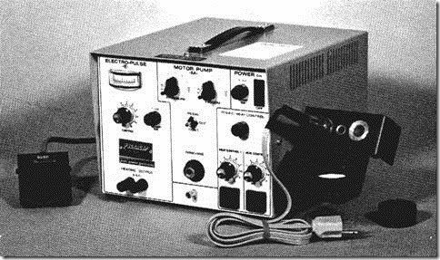
The repair station power unit is a standardized system that provides controlled soldering and desoldering of all types of solder joint configurations. The unit is shown in figure 2-1. Included in the control unit’s capabilities are:

clip_image002

Figure 2-1.—Repair station power unit.

  • · "Spike free" power switching for attached electrical hand tools to eliminate damage to electrostatic discharge components.
  • · Abrading, milling, drilling, grinding, and cutting using a flexible shaft, rotary-drive machine.

This allows the technician to remove conformal coatings, oxides, eyelets, rivets, damaged board

material, and damaged platings from assemblies.

  • · Lap flow solder connections and thermal removal of conformal coatings.
  • · Resistive and conductive tweezer heating for connector soldering applications.
  • · Thermal wire stripping for removing polyvinyl chloride (PVC) and other synethetic wire coverings.
Power Source

The basic unit houses the power supply, power level indicator, motor control switch, hand tool temperature controls, air pressure and vacuum controls with quick connect fittings, positive ground terminal, the mechanical power-drive for the rotary-drive machine, and a vacuum/pressure pump. A two- position foot pedal, to the left of the power unit in the illustration, allows hand-free operation for all ancillary (additional) handpieces. The first detent on the pedal provides power to the voltage heating outputs. The second detent activates the motor drive or vacuum/pressure pump.

Handpieces

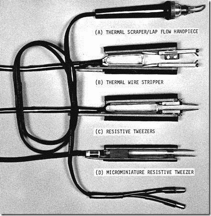
The handpieces used with the power unit are shown in figures 2-2 and 2-3. The lap flow handpiece, view (A) of figure 2-2, is used with the variable low-voltage power source. This handpiece allows removal of conformal coatings, release of sweat joints, and lap flow soldering capability. (Lap flow soldering will be discussed in topic 3.) The thermal wire stripper in view (B) is used to remove insulation from various sizes of wire easily and cleanly.

clip_image004

Figure 2-2.—Low voltage Handpiece.

clip_image006

Figure 2-3.—Motorized solder extrator.

The resistive tweezers, shown in view (C), are used for soldering components. Two sizes 176 views are provided to meet the needs of the technician. Both the thermal stripper and the resistive tweezers are used with the low-voltage power supply.

The solder extractor, shown in view (A) of figure 2-3, is connected to the variable high-voltage outlet. This handpiece allows airflow application (at controlled temperatures) of a vacuum or pressure to the selected area. Five sizes of extractor tips are provided, as shown in view (B). You can determine the one to be used by matching the tip with the circuit pad and the component being desoldered.

Soldering Irons

A soldering iron is shown in figure 2-4. This is connected to the 115-volt ac variable outlet of the power unit. You control the temperature by adjusting the voltage. The iron has replaceable tips. Chosen for their long life and good heat conductivity, soldering iron tips are high quality with iron-clad over copper construction. The tip shape and size and the heat range used are determined by the area and mass to be soldered.

clip_image008

Figure 2-4.—Soldering iron.

ROTARY-DRIVE MACHINE

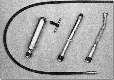
This variable-speed, rotary power drive adapts to standard diameter shank drill bits, ball mills, wheels, disks, brushes, and mandrels for most drilling and abrasive removal techniques (figure 2-5).

clip_image010

Figure 2-5.—Rotary-drive machine handpieces.

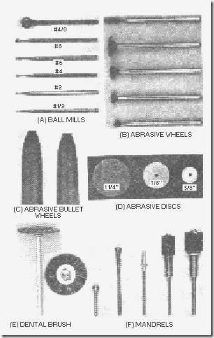
The accessories used with the rotary-drive tool are shown in views (A) through (F) of figure 2-6. Abrasive ball mills, wheels, discs, and brushes are either premounted on mandrels or can be mounted by the technician on the mandrels provided. These attachments are used for sanding and smoothing repaired areas, drilling holes, removing conformal coatings, and repairing burned or damaged areas. A chuck- equipped handpiece allows it to accept rotary tools with varying shank sizes.

clip_image011

Figure 2-6.—Rotary-drive machine accessories. BALL MILLS

CIRCUIT CARD HOLDER AND MAGNIFIER

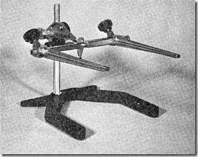
The circuit card holder is an adjustable, rotatable holder for virtually any size circuit card. Figure 2-7 shows the circuit card holder [view (A)] and the magnifier unit [view (B)]. The magnifier unit provides magnification when detail provided by a microscope is not required. The special lens allows the technician to view a rectangular area of over 14 square inches with low distortion, fine resolution, and excellent depth of field. The magnifier unit, which includes high intensity lamps, adapts to the vertical shaft of the circuit card holder.

clip_image013

Figure 2-7.—Card holder and magnifier.

HIGH-INTENSITY LIGHT

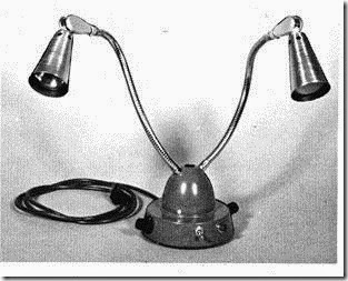
The high-intensity light provides a variable, high-intensity, portable light source over the work area. The two flexible arms permit both front and back lighting of the workpiece and provide a balanced light that eliminates shadows (figure 2-8).

clip_image015

Figure 2-8.—High intensity lamp.

The high-intensity light uses 115-volt, 60-hertz input power. One brightness knob controls a flood- type bulb, and the other knob controls a spot-type bulb.

PANA VISE

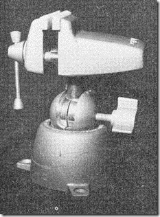
This nylon-jawed, multiposition vise can rotate and tilt. With this flexibility the technician can achieve any compound angle for holding a workpiece during assembly, modification, or repair (figure 2-9).

clip_image017

Figure 2-9.—Pana Vise.

HAND TOOLS

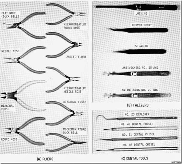
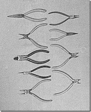
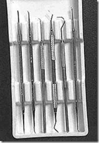
Figure 2-10, views (A) through (C), shows some representative types of hand tools used in 2M repair procedures.

clip_image019

Figure 2-10.—Pliers, tweezers, and dental tools.

Pliers

In view (A), the figure shows the pliers preferred for 2M repair procedures. These precision pliers have a long and useful life if handled and cared for properly. The flush-cutting pliers are used to cut various sizes of wire and component leads. The needlenose, roundnose, and flatnose pliers are used for forming, looping, and bending wires and component leads. They are also used for gripping components and leads during removal or installation.

clip_image021

Figure 2-10a.—Pliers.

Tweezers

View (B) shows tweezers contained in the 2M repair set. The top two pairs of tweezers are used to hold small components during installation and repair procedures. The other pairs are anti-wicking tweezers used to tin and solder stranded wire leads.

Dental Tools

View (C) shows some of the dental tools contained in the 2M repair set. They are used for picking, chipping, abrading, mixing, and smoothing various conformal coatings used on printed circuit boards and other general pcb repair techniques.

clip_image023

Figure 2-10c.—Dental tools.

Eyelet-Setting Tools

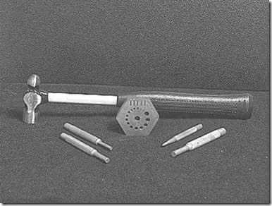
Among the repair procedures required of the 2M repair technician is the replacement of eyelets. Eyelets must sometimes be replaced because of the damage caused by incorrect repair procedures or complete failure of a printed circuit board. Figure 2-11 illustrates the tools used to replace these eyelets. Eyelets will be discussed in topic 3.

clip_image025

Figure 2-11.—Eyelet-setting tools.

MISCELLANEOUS TOOLS AND SUPPLIES

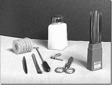
An assortment of some of the miscellaneous items used in 2M repair are shown in figure 2-12. A variety of brushes, files, scissors, thermal shunts, and consumables, such as solder wick, are included.

Even though all the items are not used in every repair procedure, it is extremely important that they be available for use should the need arise.

clip_image027

Figure 2-12.—Miscellaneous tools and supplies.

SAFETY EQUIPMENT

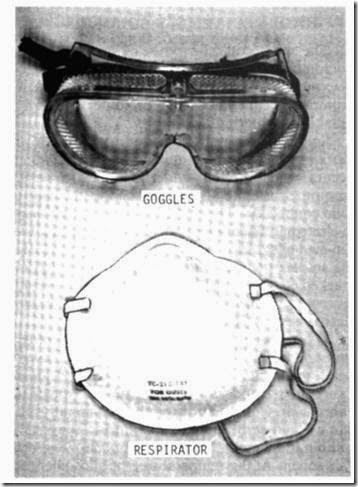
The nature of 2M repair requires items to be included in the tool kit for the personal safety of the technicians. The goggles and respirator illustrated in figure 2-13 have been approved for use by the technician. These should be worn at all times where dust, chips, fumes, and other hazardous substances are generated as a result of drilling, grinding, or other repair procedures.

clip_image029

Figure 2-13.—Safety equipment.

STEREOSCOPIC-ZOOM MICROSCOPE

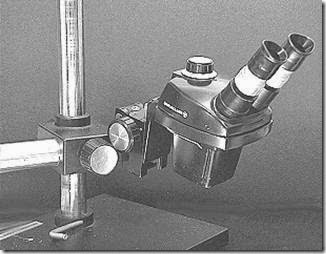
The stereoscopic-zoom microscope provides a versatile optical viewing system. This viewing system is used in the fault detection, fault isolation, and repair of complex microminiature circuit boards and components. Figure 2-14 shows the microscope mounted on an adjustable stand. The microscope has a minimum of 3.5X and a maximum of 30X magnification to detect hairline cracks in conductor runs and stress cracks in solder joints.

clip_image031

Figure 2-14.—Stereoscopic zoom microscope.

TOOL CHEST

The tool chest (not shown), provides storage space for the electronic repair hand tools, dental tools, abrasive wheels, solder and solder wicks, eyelets, abrasive disks, ball mills, various burrs, and other consumables used with the repair procedures. The chest is portable, lockable, and has variously sized drawers for convenience.

REPLACEMENT PARTS

Replacement parts are provided with the 2M repair set to ensure the technician has the capability to maintain the equipment properly. Actual preventive and corrective maintenance procedures, as well as data on additional spare parts and ordering information, are found in the technical manual for the 2M repair set equipment.

REPAIR STATION FACILITIES

To be effective, 2M electronic component repair must be performed under proper environmental conditions. Repair facility requirements, whether afloat or ashore, include adequate lighting, ventilation, noise considerations, work surface area, ESD (electrostatic discharge) protection, and adequate power availability. The recommended environmental conditions are discussed below. With the exception of requirements imposed by the Naval Environmental Health Center and other authorities for ship and shore work conditions, each activity tailors the requirements to meet local needs.

LIGHTING

The recommended lighting for a work surface is 100 footcandles from a direct lighting source. Light- colored overheads and bulkheads and off-white or pastel workbench tops are used to complement the lighting provided.

VENTILATION

Fumes from burning flux, coating materials, grinding dust, and cleaning solvents require adequate ventilation. The use of toxic, flammable substances, solvents, and coating compounds requires a duct system that vents gasses and vapors. This type of system must be used to prevent contamination often

found in closed ventilation systems. This need is particularly important aboard ship. Vented hoods, ducts, or installations that are vented outside generally meet the minimum standards set by the Naval Environmental Health Center.

NOISE CONSIDERATIONS

Noise in the work area during normal work periods must be no greater than the acceptable level approved for each activity involved. Because the work is tedious and tiring, noise levels should be as low as possible. Ear protectors are required to be worn when a noise level exceeds 85 dB. Ear protectors should also be worn anytime the technician feels distracted by, or uncomfortable with, the noise level.

WORK SURFACE AREA

Work stations should have a minimum work surface of at least 60-inches wide and 30-inches deep. Standard Navy desks are excellent for this purpose. Standard shipboard workbenches are acceptable; however, off-white or pastel-colored heat-resistant tops should be installed on the workbenches. Chairs should be the type with backs and without arms. They should be comfortably padded and of the proper height to match the work surface height. Drawers or other suitable tool storage areas are usually provided.

ELECTROSTATIC DISCHARGE SENSITIVE DEVICE (ESDS) CAPABILITY

A 2M work station should be capable of becoming a static-free work station. This is specified in the Department of Defense Standard, Electrostatic DISCHARGE Control Program for Protection of Electrical and Electronic Parts, Assemblies, and Equipment. ESD will be discussed in greater detail in topic 3.

POWER REQUIREMENTS

No special power source or equipment mounting is required. The 2M repair equipment operates on 115-volt, 60-hertz power. A 15-ampere circuit is sufficient and six individual power receptacles should be available.

HIGH-RELIABILITY SOLDERING

The most common types of miniature and microminiature repair involve the removal and replacement of circuit components. The key to these repairs is a firm knowledge of solder and high- reliability soldering techniques.

Solder is a metal alloy used to join two or more metals with a metallic bond. The bonding occurs when molten solder dissolves a small amount of the metals and then cools to form a solid connection. The solder most commonly used in electronic assemblies is an alloy of tin and lead. Tin-lead alloys are identified by their percentage in the solder; the tin content is given first. Solder marked 60/40 is an alloy of 60 percent tin and 40 percent lead. The two most common alloys used in electronics are 60/40 and 63/37.

The melting temperature of tin-lead solder varies depending on the percentage of each metal. Lead melts at a temperature of 621 degrees Fahrenheit, and tin melts at 450 degrees Fahrenheit. Combinations of the two metals melt into a liquid at different temperatures. The 63/37 combination melts into a liquid at 361 degrees Fahrenheit. At this temperature, the alloy changes from a solid directly to a liquid with no plastic or semiliquid state. An alloy with such a sharp changing point is called a EUTECTIC ALLOY.

As the percentages of tin and lead are varied, the melting temperature increases. Alloy of 60/40 melts at 370 degrees Fahrenheit, and alloy of 70/30 melts at approximately 380 degrees Fahrenheit. Alloys, other than eutectic, go through a plastic or semiliquid state in their heating and cooling stages. Solder joints that are disturbed (moved) during the plastic state will result in damaged connections. For this reason, 63/37 solder is the best alloy for electronic work. Solder with 60/40 alloy is also acceptable, but it goes into a plastic state between 361 and 370 degrees Fahrenheit. When soldering joints with 60/40 alloy, you must exercise extreme care to prevent movement of the component during cooling.

USE OF FLUX IN SOLDER BONDING

Reliable solder connections can only be accomplished with clean surfaces. Using solvents and abrasives to clean the surfaces to be soldered is essential if you are to achieve good solder connections. In almost all cases, however, this cleaning process is insufficient because oxides form rapidly on heated metal surfaces. The rapid formation of oxides creates a nonmetallic film that prevents solder from contacting the metal. Good metal-to-metal contact must be obtained before good soldering joints may take place. Flux removes these surface oxides from metals to be soldered and keeps them removed during the soldering operation. Flux chemically breaks down surface oxides and causes the oxide film to loosen and break free from the metals being soldered.

Soldering fluxes are divided into three classifications or groups: CHLORIDE FLUX (commonly called ACID), ORGANIC FLUX, and ROSIN FLUX. Each flux has characteristics specific to its own group. Chloride fluxes are the most active of the three groups. They are effective on all common metals except aluminum and magnesium. Chloride fluxes, however, are NOT suitable for electronic soldering because they are highly corrosive, electrically conductive, and are difficult to remove from the soldered joint.

Organic fluxes are nearly as active as chloride fluxes, yet are less corrosive and easier to remove than chloride fluxes. Also, these fluxes are NOT satisfactory for electronic soldering because they must be removed completely to prevent corrosion.

Rosin fluxes ARE ideally suited to electronic soldering because of their molecular structure. The most common flux used in electronic soldering is a solution of pure rosin dissolved in suitable solvent. This solution works well with the tin- or solder-dipped metals commonly used for wires, lugs, and connectors. While inert at normal temperatures, rosin fluxes break down and become highly active at soldering temperatures. In addition, rosin is nonconductive.

Most electronic solder, in wire form, is made with one or more cores of rosin flux. When the joint or connection is heated and the wire solder is applied to the joint (not the iron), the flux flows onto the surface of the joint and removes the oxide. This process aids the wetting action of the solder. With enough heat the solder flows and replaces the flux. Insufficient heat results in a poor connection because the solder does not replace the flux.

Q10. Stereoscopic-zoom microscopes and precision drill presses are normally associated with what type of repair station?

Q11. Solder used in electronic repair is normally an alloy of what two elements? Q12. In soldering, what alloy changes directly from a solid state to a liquid state? Q13. Flux aids in soldering by removing what from surfaces to be soldered?

Q14. What type(s) of flux should never be used on electronic equipment?


Answers to Questions and Summary of Miniature/Micro miniature (2m) Repair Program and High-Reliability Soldering.

SUMMARY

This topic has presented information on the Miniature and Microminiature 2M Repair Program and high-reliability soldering. The information that follows summarizes the important points of this topic.

The MINIATURE/MICROMINIATURE (2M) REPAIR PROGRAM provides training, tools and equipment, and certification for 2M repair personnel.

CERTIFICATION of technicians ensures the capability of high-quality, high-reliability repairs. The three SM&R codes for maintenance of electronic devices are: DEPOT (D),

INTERMEDIATE (I), and ORGANIZATIONAL (O).

SM&R CODE D MAINTENANCE is characterized by extensive facilities and highly trained personnel. Code D activities are capable of the most complex type repairs.

CODE I activities provide direct support for user activities. This includes calibration, repair, and emergency manufacture of nonavailable parts.

CODE O maintenance is the responsibility of the user activity. It includes preventive maintenance and minor repairs.

ON-LINE TEST EQUIPMENT continuously monitors system performance and isolates faults to removable assemblies.

OFF-LINE TEST EQUIPMENT evaluates removable assemblies outside of the equipment and isolates faults to the component level.

FAULT ISOLATION USING GENERAL-PURPOSE ELECTRONIC TEST EQUIPMENT

(GPETE) should only be attempted by experienced technicians.

2M REPAIR STATIONS are equipped according to the level of repairs to be accomplished.

ALLOYS, such as solder, which change directly from a solid state to a liquid are called eutectic alloys.

SOLDER with a tin/lead ratio of 63/37 is preferred for electronic work. A ratio of 60/40 is also acceptable.

ROSIN or RESIN FLUXES are the only fluxes to be used in electronic work.

ANSWERS TO QUESTIONS Q1. THROUGH Q14.

A1. Chief of Naval Operations (CNO).

A2. Naval Sea Systems Command (NAVSEASYSCOM) and Naval Air Systems Command (NAVAIRSYSCOM).

A3. Microminiature component repair.

A4. Microminiature repair technician.

A5. Depot, Intermediate, and Organizational.

A6. Organizational.

A7. On-line, off-line, and General Purpose Electronic Test Equipment (GPETE).

A8. On-line.

A9. Off-line.

A10. Microminiature repair station.

A11. Tin and lead.

A12. Eutectic.

A13. Oxides.

A14. Chloride or (acid) and organic.


Answers to Questions and Summary of Microelectronics.

SUMMARY

This topic has presented information on the development and manufacture of microelectronic devices. The information that follows summarizes the important points of this topic.

VACUUM-TUBE CIRCUITS in most modern military equipment are unacceptable because of size, weight, and power use.

Discovery of the transistor in 1948 marked the beginning of MICROELECTRONICS.

The PRINTED CIRCUIT BOARD (pcb) reduces weight and eliminates point-to-point wiring.

clip_image002

The INTEGRATED CIRCUITS (IC) consist of elements inseparably associated and formed on or within a single SUBSTRATE.

ICs are classified as three types: MONOLITHIC, FILM, and HYBRID.

The MONOLITHIC IC, called a chip or die, contains both active and passive elements.

clip_image003

FILM COMPONENTS are passive elements, either resistors or capacitors.

HYBRID ICs are combinations of monolithic and film or of film and discrete components, or any combination thereof. They allow flexibility in circuits.

clip_image005

Rapid development has resulted in increased reliability and availability, reduced cost, and higher element density.

LARGE-SCALE (lsi) and VERY LARGE-SCALE INTEGRATION (vlsi) allow thousands of elements in a single chip.

MONOLITHIC ICs are produced by the diffusion or epitaxial methods.

DIFFUSED elements penetrate the substrate, EPITAXIAL do not.

clip_image007

ISOLATION is a production method to prevent unwanted interaction between elements within a chip.

THIN-FILM ELEMENTS are produced through EVAPORATION or CATHODE SPUTTERING techniques.

THICK-FILM ELEMENTS are screened onto the substrate.

The most common types of packages for ICs are TO, FLAT PACK, and DUAL INLINE.

clip_image009

FLIP CHIPS and BEAM-LEAD CHIPS are techniques being developed to eliminate bonding wires and to improve packaging.

clip_image011

clip_image013

Large DIPs are being used to package lsi and vlsi. They can be produced with up to 64 pins and are designed to fulfill a specific need.

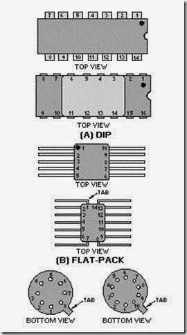
Viewed from the tops, DIPS and FLAT-PACK LEADS are numbered counterclockwise from the reference mark.

Viewed from the bottom, TO-5 LEADS are numbered clockwise from the tab.

clip_image015

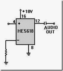
Numbers and letters on schematics and ICs identify the TYPE OF IC.

clip_image017

Knowledge of TERMINOLOGY used in microelectronics and of packaging concepts will aid you in becoming an effective technician.

STANDARD TERMINOLOGY has been adopted by the Navy to ease communication.

MICROELECTRONICS is that area of technology associated with electronic systems designed with extremely small parts or elements.

A MICROCIRCUIT is a small circuit which is considered as a single part composed of elements on or within a single substrate.

clip_image018

A MICROCIRCUIT MODULE is an assembly of microcircuits or a combination of microcircuits and discrete components packaged as a replaceable unit.

MINIATURE ELECTRONICS are card assemblies and modules composed exclusively of discrete electronic components.

SYSTEM PACKAGING refers to the design of a system, taking into account environmental and electronic characteristics, access, and maintainability.

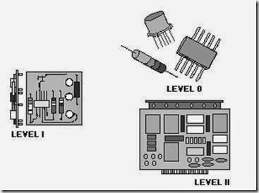
PACKAGING LEVELS 0 to IV are used to identify assemblies within a system. Packaging levels are as follows:

LEVEL 0-Nonrepairable parts (resistors, diodes, and so forth.)

LEVEL I -Submodules attached to circuit cards.

LEVEL II -Circuit cards and MOTHER BOARDS.

clip_image020

LEVEL III – Drawers.

clip_image022

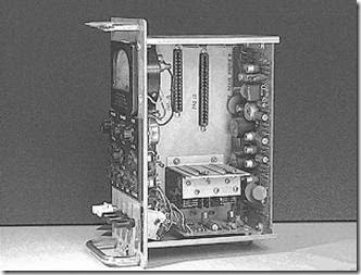
LEVEL IV – Cabinets.

clip_image024

The most common METHODS OF INTERCONNECTION are the conventional pcb, the multilayer pcb, and modular assemblies.

clip_image026

Three methods of interconnecting circuitry in multilayer printed circuit boards are the

CLEARANCE-HOLE, the PLATED-THROUGH-HOLE, and LAYER BUILD-UP.

MODULAR ASSEMBLIES were devised to achieve high circuit density. Modular assemblies have progressed from CORDWOOD MODULES through

MICROMODULES. Micromodules consist of film components and discrete components to integrated and hybrid circuitry.

ENVIRONMENTAL FACTORS to be considered are temperature, humidity, shock, vibration, and rf interference.

clip_image028

ELECTRICAL FACTORS are overcome by using shielding and ground planes and by careful placement of components.

clip_image030

ANSWERS TO QUESTIONS Q1. THROUGH Q50.

A1. Size, weight, and power consumption. A2. The transistor and solid-state diode.

A3. Technology of electronic systems made of extremely small electronic parts or elements. A4. The Edison Effect.

A5. Transformers, capacitors, and resistors.

A6. "Rat’s nest" appearance and unwanted interaction, such as capacitive and inductive effects. A7. Rapid repair of systems and improved efficiency.

A8. Differences in performance of tubes of the same type. A9. Eliminate heavy chassis and point-to-point wiring. A10. Components soldered in place.

A11. Cordwood module.

A12. Elements inseparably associated and formed in or on a single substrate. A13. Monolithic, film, and hybrid.

A14. Monolithic ICs contain active and passive elements. Film ICs contain only passive elements.

A15. Combination of monolithic ICs and film components. A16. 1,000 to 2,000.

A17. Circuit design, component placement, suitable substrate, and depositing proper materials on substrate.

A18. Complex.

A19. Control patterns of materials on substrates. A20. Glass or ceramic.

A21. Crystal is sliced into wafers. Then ground and polished to remove any surface defect. A22. Diffusion; epitaxial growth.

A23. Diffusion penetrates substrate; epitaxial does not. A24. Electrical separation of elements.

A25. Evaporation and cathode sputtering. A26. Screening.

A27. Combination of monolithic and film elements. A28. Circuit flexibility.

A29. Protect the IC from damage; make handling easier. A30. TO, flat pack, DIP.

A31. Flip-chip, beam lead. A32. Left.

A33. Counterclockwise. A34. Reference mark. A35. Clockwise.

A36. Identify the type of IC. A37. Communication. A38. Integrated circuits. A39. Miniature.

A40. Level 0. A41. Level I. A42. Level II.

A43. Conventional printed circuit boards, multilayer printed circuit boards and modular assemblies. A44. Clearance hole, plated-through hole, and layer build-up.

A45. Difficulty of repair of internal connections. A46. Cordwood modules.

A47. Procurement specifications. A48. Military Standards.

A49. Equipment designers (planners).

A50. Ground planes, shielding, component placement.


Miniature/Micro miniature (2m) Repair Program and High-Reliability Soldering.

MINIATURE/MICROMINIATURE (2M) REPAIR PROGRAM AND HIGH-RELIABILITY SOLDERING

LEARNING OBJECTIVES

Upon completion of this topic, the student will be able to:

1. State the purpose and need for training and certification of 2M repair technicians.

2. Explain the maintenance levels at which maintenance is performed.

3. Identify the specialized and general test equipment used in fault isolation.

4. Recognize the specialized types of tools used and the importance of repair facilities.

5. Explain the principles of high-reliability soldering.

INTRODUCTION

As mentioned in topic 1, advances in the field of microelectronics are impressive. With every step forward in production development, a corresponding step forward must be made in maintenance and repair techniques.

This topic will teach you how the Navy is coping with the new technology and how personnel are trained to carry out the maintenance and repair of complex equipment. The program discussed in this topic is up to date at this time, but as industry advances, so must the capabilities of the technician.

MINIATURE AND MICROMINIATURE (2M) ELECTRONIC REPAIR PROGRAM

Training requirements for miniature and microminiature repair personnel were developed under guidelines established by the Chief of Naval Operations. The Naval Sea Systems Command (NAVSEA) developed a program which provides for the proper training in miniature and microminiature repair. This program, NAVSEA Miniature/Microminiature (2M) Electronic Repair, authorizes and provides proper tools and equipment and establishes a personnel certification program to maintain quality repair.

The Naval Air Systems Command has developed a similar program specifically for the aviation community. The two programs are patterned after the National Aeronautics and Space Administration (NASA) high-reliability soldering studies and have few differences other than the administrative chain of command. For purposes of this topic, we will use the NAVSEA manual for reference.

The 2M program covers all phases of miniature and microminiature repair. It establishes the training curriculum for repair personnel, outlines standards of workmanship, and provides guidelines for specific repairs to equipment, including the types of tools to use. This part of the program ensures high-reliability repairs by qualified technicians.

Upon satisfactory completion of a 2M training course, a technician will be CERTIFIED to perform repairs. The CERTIFICATION is issued at the level at which the technician qualifies and specifies what type of repairs the technician is permitted to perform. The two levels of qualification for technicians are MINIATURE COMPONENT REPAIR and MICROMINIATURE COMPONENT REPAIR. Miniature

component repair is limited to discrete components and single- and double-sided printed circuit boards, including removal and installation of most integrated circuit devices. Microminiature component repair consists of repairs to highly complex, densely packaged, multilayer printed circuit boards. Sophisticated repair equipment is used that may include a binocular microscope.

To ensure that a technician is maintaining the required qualification level, periodic evaluations are conducted. By inspecting and evaluating the technician’s work, certification teams ensure that the minimum standards for the technician’s level of qualification are met. If the standards are met, the technician is recertified; if not, the certification is withheld pending retraining and requalification. This portion of the program ensures the high-quality, high-reliability repairs needed to meet operational requirements.

Q1. Training requirements for (2M) repair personnel were developed under guidelines established by what organization?
Q2. What agencies provide training, tools, equipment, and certification of the 2M system?

Q3. To perform microminiature component repair, a 2M technician must be currently certified in what area?

Q4. Multilayer printed circuit board repair is the responsibility of what 2M repair technician?

LEVELS OF MAINTENANCE

Effective maintenance and repair of microelectronic devices require one of three levels of maintenance. Level-of-repair designations called SOURCE, MAINTENANCE, and RECOVERABILITY CODES (SM&R) have been developed and are assigned by the Chief of Naval Material. These codes are D for DEPOT LEVEL, I for INTERMEDIATE LEVEL, and O for ORGANIZATIONAL LEVEL.

DEPOT-LEVEL MAINTENANCE.

SM&R Code D maintenance is the responsibility of maintenance activities designated by the systems command (NAVSEA, NAVAIR, NAVELEX). This code augments stocks of serviceable material. It also supports codes I and O activities by providing more extensive shop facilities and equipment and more highly skilled technicians. Code D maintenance includes repair, modification, alteration, modernization, and overhaul as well as reclamation or reconstruction of parts, assemblies, subassemblies, and components. Finally, it includes emergency manufacture of nonavailable parts. Code D maintenance also provides technical assistance to user activities and to code I maintenance organizations. Code D maintenance is performed in shops, located in shipyards and shore-based facilities, including contractor maintenance organizations.

INTERMEDIATE-LEVEL MAINTENANCE

SM&R code I maintenance, performed at mobile shops, tenders or shore-based repair facilities (SIMAS) provides direct support to user organizations. Code I maintenance includes calibration, repair, or replacement of damaged or unserviceable parts, components, or assemblies, and emergency manufacture of nonavailable parts. It also provides technical assistance to ships and stations.

ORGANIZATIONAL-LEVEL MAINTENANCE

SM&R code O maintenance is the responsibility of the activity who owns the equipment. Code O maintenance consists of inspecting, servicing, lubricating, adjusting, and replacing parts, minor assemblies, and subassemblies.

An INTEGRATED LOGISTICS SUPPORT PLAN (ILSP) determines the maintenance level for electronic assemblies, modules, and boards for each equipment assigned to an activity. The ILSP codes the items according to the normal maintenance capabilities of that activity. This results in two additional repair-level categories – NORMAL and EMERGENCY.

Normal Repairs

Generally, 2M repairs are performed at the level set forth in the maintenance plan and specified by the appropriate SM&R coding for each board or module. Therefore, normal repairs include all repairs except organizational-level repair of D- and I-coded items and intermediate-level repair of D-coded items.

Emergent/Emergency Repairs

In the NAVSEA 2M Electronic Repair Program, emergent/emergency repairs are those arising unexpectedly. They may require prompt repair action to restore a system or piece of equipment to operating condition where normal repairs are not authorized. These Code O repairs on boards or modules are normally SM&R-coded for Code D repairs. Emergent/emergency 2M repairs may be performed only to meet an urgent operational commitment as directed by the operational commander.

SOURCE, MAINTENANCE, AND RECOVERABILITY (SM&R) CODES

The Allowance Parts List (APL) is a technical document prepared by the Navy for specific equipment/system support. This document lists the repair parts requirements for a ship having the exact equipment/component. To determine the availability of repair parts, the 2M technician must be familiar with these documents. SM&R codes, found in APLs, determine where repair parts can be obtained, who is authorized to make the repair, and at what maintenance level the item may be recovered or condemned.

Q5. What are the three levels of maintenance?

Q6. Maintenance performed by the user activity is what maintenance level?


Microelectronics: Interconnections In Printed Circuit Boards, Modular Assemblies, Environmental Considerations and Electrical Considerations.

INTERCONNECTIONS IN PRINTED CIRCUIT BOARDS

As electronic systems become more complex, interconnections between components also becomes more complex. As more components are added to a given space, the requirements for interconnections become extremely complicated. The selection of conductor materials, insulator materials, and component physical size can greatly affect the performance of the circuit. Poor choices of these materials can contribute to poor signals, circuit noise, and unwanted electrical interaction between components. The three most common methods of interconnection are the conventional pcb, the multilayer pcb, and the modular assembly. Each of these will be discussed in the following sections.

Conventional Printed Circuit Board

Printed circuit boards were discussed earlier in topic 1. You should recall that a conventional pcb consists of glass-epoxy insulating base on which the interconnecting pattern has been etched. The board may be single- or double-sided, depending on the number of components mounted on it. Figures 1-37 and 1-38 are examples of conventional printed circuit boards.

Multilayer Printed Circuit Board.

The multilayer printed circuit board is emerging as the solution is interconnection problems associated with high-density packaging. Multilayer boards are used to:

  • · reduce weight
  • · conserve space in interconnecting circuit modules
  • · eliminate costly and complicated wiring harnesses
  • · provide shielding for a large number of conductors
  • · provide uniformity in conductor impedance for high-speed switching systems
  • · allow greater wiring density on boards

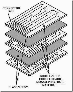
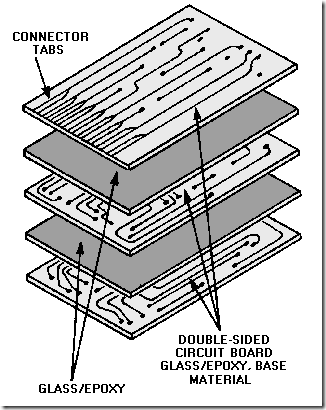
Figure 1-39 illustrates how individual boards are mated to form the multilayer unit. Although all multilayer boards are similarly constructed, various methods can be used to interconnect the circuitry from layer to layer. Three proven processes are the clearance-hole, plated-through hole, and layer build- up methods.

clip_image001

Figure 1-39.—Multilayer pcb.

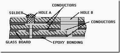
CLEARANCE-HOLE METHOD.—In the CLEARANCE-HOLE method, a hole is drilled in the copper island (terminating end) of the appropriate conductor on the top layer. This provides access to a conductor on the second layer as shown by hole A in figure 1-40. The clearance hole is filled with solder to complete the connection. Usually, the hole is drilled through the entire assembly at the connection site. This small hole is necessary for the SOLDER-FLOW PROCESS used with this interconnection method.

clip_image003

Figure 1-40.—Clearance-hole interconnection.

Conductors located several layers below the top are connected by using a STEPPED-DOWN HOLE PROCESS. Before assembly of a three-level board, a clearance hole is drilled down to the first layer to be interconnected. The first layer to be interconnected is predrilled with a hole smaller than those drilled in layers 1 and 2; succeeding layers to be connected have progressively smaller clearance holes. After assembly, the exposed portion of the conductors are interconnected by filling the stepped-down holes with solder, as shown by hole B in figure 1-40. The larger the number of interconnections required at one point, the larger must be the diameter of the clearance holes on the top layer. Large clearance holes on the top layer allow less space for components and reduce packaging density.

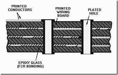
PLATED-THROUGH-HOLE METHOD.—The PLATED-THROUGH-HOLE method of

interconnecting conductors is illustrated in figure 1-41. The first step is to temporarily assemble all the layers into their final form. Holes corresponding to required connections are drilled through the entire

assembly and then the unit is disassembled. The internal walls of those holes to be interconnected are plated with metal which is 0.001 inch thick. This, in effect, connects the conductor on the board surface

through the hole itself. This process is identical to that used for standard printed circuit boards. The boards are then reassembled and permanently bonded together with heat and pressure. All the holes are plated through with metal.

clip_image005

Figure 1-41.—Plated through-hole interconnection.

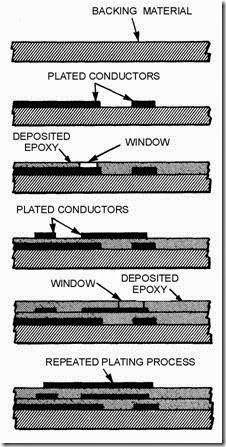
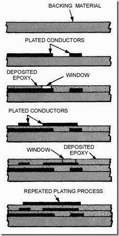
LAYER BUILD-UP METHOD.—With the LAYER BUILD-UP method, conductors and insulation layers are alternately deposited on a backing material, as shown in figure 1-42. This method produces copper interconnections between layers and minimizes the thermal expansion effects of dissimilar materials. However, reworking the internal connections in built-up layers is usually difficult, if not impossible.

clip_image007

Figure 1-42.—Layer build-up technique.

Advantages and Disadvantages of Printed Circuit Boards

Some of the advantages and disadvantages of printed circuit boards were discussed earlier in this topic. They are strong, lightweight, and eliminate point-to-point wiring. Multilayer printed circuit boards allow more components per card. Entire circuits or even subsystems may be placed on the same card. However, these cards do have some drawbacks. For example, all components are wired into place, repair of cards requires special training and/or special equipment, and some cards cannot be economically repaired because of their complexity (these are referred to as THROWAWAYS).

MODULAR ASSEMBLIES

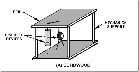
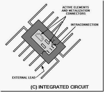
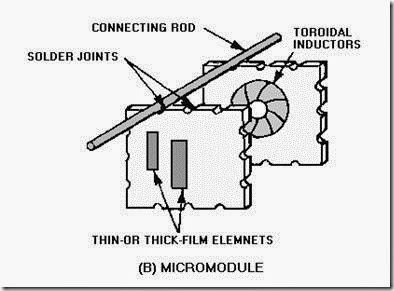
The MODULAR-ASSEMBLY (nonrepairable item) approach was devised to achieve ultra-high density packaging. The evolution of this concept, from discrete components to microelectronics, has progressed through various stages. These stages began with cordwood assemblies and functional blocks and led to complete subsystems in a single package. Examples of these configurations are shown in figure 1-43, view (A), view (B), and view (C).

clip_image008

Figure 1-43A.—Evolution of modular assemblies. CORDWOOD.

clip_image010

Figure 1-43B.—Evolution of modular assemblies. MICROMODULE.

clip_image012

Figure 1-43C.—Evolution of modular assemblies. INTEGRATED-CIRCUIT.

Cordwood Modules.

The cordwood assembly, shown in view (A) of figure 1-43, was designed and fabricated in various forms and sizes, depending on user requirements. This design was used to reduce the physical size and increase the component density and complexity of circuits through the use of discrete devices. However, the use of the technique was somewhat limited by the size of available discrete components used.

Micromodules

The next generation assembly was the micromodule. Designers tried to achieve maximum density in this design by using discrete components, thick- and thin-film technologies, and the insulator substrate principle. The method used in this construction technique allowed for the efficient use of space and also provided the mechanical strength necessary to withstand shock and vibration.

Semiconductor technology was then improved further with the introduction of the integrated circuit. The flat-pack IC form, shown in view (C), emphasizes the density and complexity that exists with this technique. This technology provides the means of reducing the size of circuits. It also allows the reduction of the size of systems through the advent of the lsi circuits that are now available and vlsi circuits that are being developed by various IC manufacturers.

Continuation of this trend toward microminiaturization will result in system forms that will require maintenance personnel to be specially trained in maintenance techniques to perform testing, fault isolation, and repair of systems containing complex miniature and microminiature circuits.

Q43. What are the three most common methods of interconnections?

Q44. Name the three methods of interconnecting components in multilayer printed circuit boards. Q45. What is one of the major disadvantages of multilayer printed circuit boards?

Q46. What was the earliest form of micromodule?

ENVIRONMENTAL CONSIDERATIONS

The environmental requirements of each system design are defined in the PROCUREMENT SPECIFICATION. Typical environmental requirements for an IC, for example, are shown in table 1-1. After these system requirements have been established, components, applications, and packaging forms are considered. This then leads to the most effective system form.

image

In the example in table 1-1, the environmental requirements are set forth as MILITARY STANDARDS for performance. The actual standard for a particular factor is in parentheses. To meet each of these standards, the equipment or component must perform adequately within the test guidelines. For example, to pass the shock test, the component must withstand a shock of 250 to 600 Gs (force of gravity). During vibration testing, the component must withstand vibrations of 5 to 15 cycles per second for 0.06 day, or about 1 1/2 hours; 16 to 25 cycles for 1 hour; and 26 to 33 cycles for 1/2 hour. Rf interference between 30 hertz and 40 gigahertz must not affect the performance of the component. Temperature and humidity factors are self-explanatory.

When selecting the most useful packaging technique, the system designer must consider not only the environmental and electrical performance requirements of the system, but the maintainability aspects as well. The system design will, therefore, reflect performance requirements of maintenance and repair personnel.

ELECTRICAL CONSIDERATIONS

The electrical characteristics of a component can sometimes be adversely affected when it is placed in a given system. This effect can show up as signal distortion, an improper timing sequence, a frequency shift, or numerous other types of unwanted interactions. Techniques designed to minimize the effects of system packaging on component performance are incorporated into system design by planners. These techniques should not be altered during your maintenance. Several of the techniques used by planners are discussed in the following sections.

Ground Planes and Shielding.

At packaging levels I and II, COPPER PLANES with voids, where feed-through is required, can be placed anywhere within the multilayer board. These planes tend to minimize interference between circuits and from external sources.

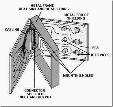
At other system levels, CROSS TALK (one signal interfering with another), rf generation within the system, and external interference are suppressed through the use of various techniques. These techniques

are shown in figure 1-44. As shown in the figure, rf shielding is used on the mating surfaces of the package, cabling is shielded, and heat sinks are provided.

clip_image013

Figure 1-44.—Ground planes and shielding.

Interconnection and Intraconnections

To meet the high-frequency characteristics and propagation timing required by present and future systems, the device package must not have excessive distributed capacitance and/or inductance. This type of packaging is accomplished in the design of systems using ICs and other microelectronic devices by using shorter leads internal to the package and by careful spacing of complex circuits on printed circuit boards. To take advantage of the inherent speed of the integrated circuit, you must keep the signal propagation time between circuits to a minimum. The signal is delayed approximately 1 nanosecond per foot, so reducing the distance between circuits as much as possible is necessary. This requires the use of structures, such as high-density digital systems with an emphasis on large-scale integration, for systems in the future. Also, maintenance personnel should be especially concerned with the spacing of circuits, lead dress, and surface cleanliness. These factors affect the performance of high-speed digital and analog circuits.

Q47. In what publication are environmental requirements for equipment defined?

Q48. In what publication would you find guidelines for performance of military electronic parts? Q49. Who is responsible for meeting environmental and electrical requirements of a system? Q50. What methods are used to prevent unwanted component interaction?


Microelectronics: Microelectronic System Design Concepts, Terminology and System Packaging.

MICROELECTRONIC SYSTEM DESIGN CONCEPTS

You should understand the terminology used in microelectronics to become an effective and knowledgeable technician. You should be familiar with packaging concepts from a maintenance standpoint and be able to recognize the different types of assemblies. You should also know the electrical and environmental factors that can affect microelectronic circuits. In the next section of this topic we will define and discuss each of these areas.

TERMINOLOGY

As in any special electronics field, microelectronics terms and definitions are used to clarify communications. This is done so that everyone involved in microelectronics work has the same knowledge of the field. You can imagine how much trouble you would have remembering 10 or more different names and definitions for a resistor. If standardization didn’t exist for the new terminology, you would have far more trouble understanding microelectronics. To standardize terminology in microelectronics, the Navy has adopted several definitions with which you should become familiar. These definitions will be presented in this section.

Microelectronics

Microelectronics is that area of electronics technology associated with electronics systems built from extremely small electronic parts or elements. Most of today’s computers, weapons systems, navigation systems, communications systems, and radar systems make extensive use of microelectronics technology.

Microcircuit

A microcircuit is not what the old-time technician would recognize as an electronic circuit. The old- timer would no longer see the familiar discrete parts (individual resistors, capacitors, inductors, transistors, and so forth). Microelectronic circuits, as discussed earlier, are complete circuits mounted on a substrate (integrated circuit). The process of fabricating microelectronic circuits is essentially one of building discrete component characteristics either into or onto a single substrate. This is far different from soldering resistors, capacitors, transistors, inductors, and other discrete components into place with wires and lugs. The component characteristics built into microcircuits are referred to as ELEMENTS rather than discrete components. Microcircuits have a high number of these elements per substrate compared to a circuit with discrete components of the same relative size. As a matter of fact, microelectronic circuits often contain thousands of times the number of discrete components. The term HIGH EQUIVALENT CIRCUIT DENSITY is a description of this element-to-discrete part relationship. For example, suppose you have a circuit with 1,000 discrete components mounted on a chassis which is 8 ´ 10 ´ 2 inches. The equivalent circuit in microelectronics might be built into or onto a single substrate which is only 3/8 x 1 x 1/4 inch. The 1,000 elements of the microcircuit would be very close to each other (high density) by comparison to the distance between discrete components mounted on the large chassis. The elements within the substrate are interconnected on the single substrate itself to perform an electronic function. A microcircuit does not have any discrete components mounted on it as do printed circuit boards, circuit card assemblies, and modules composed exclusively of discrete component parts.

Microcircuit Module

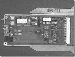
Microcircuits may be used in combination with discrete components. An assembly of microcircuits or a combination of microcircuits and discrete conventional electronic components that performs one or more distinct functions is a microcircuit module. The module is constructed as an independently packaged, replaceable unit. Examples of microcircuit modules are printed circuit boards and circuit card assemblies. Figure 1-35 is a photograph of a typical microcircuit module.

clip_image002

Figure 1-35.—Microcircuit module.

Miniature Electronics

Miniature electronics includes miniature electronic components and packages. Some examples are printed circuit boards, printed wiring boards, circuit card assemblies, and modules composed exclusively of discrete electronic parts and components (excluding microelectronic packages) mounted on boards, assemblies, or modules. MOTHER BOARDS, large printed circuit boards with plug-in modules, are considered miniature electronics. Cordwood modules also fall into this category. Miniature motors, synchros, switches, relays, timers, and so forth, are also classified as miniature electronics.

Recall that microelectronic components contain integrated circuits. Miniature electronics contain discrete elements or parts. You will notice that printed circuit boards and circuit card assemblies are mentioned in more than one definition. To identify the class (microminiature or miniature) of the unit, you must first determine the types of components used.

Q37. Standardized terms improve what action between individuals?

Q38. Microcircuit refers to any component containing what types of elements?

Q39. Components made up exclusively of discrete elements are classified as what type of electronics?

SYSTEM PACKAGING

When a new electronics system is developed, several areas of planning require special attention. An area of great concern is that of ensuring that the system performs properly. The designer must take into account all environmental and electrical factors that may affect the system. This includes temperature, humidity, vibration, and electrical interference. The design factor that has the greatest impact on you, as the technician, is the MAINTAINABILITY of the system. The designer must take into account how well you will be able to locate problems, identify the faulty components, and make the necessary repairs. If a system cannot be maintained easily, then it is not an efficient system. PACKAGING, the method of enclosing and mounting components, is of primary importance in system maintainability.

Levels of Packaging

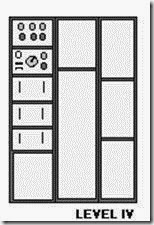
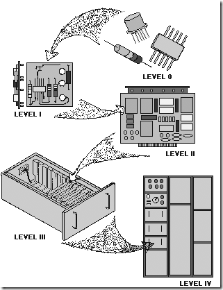
For the benefit of the technician, system packaging is usually broken down to five levels (0 to IV). These levels are shown in figure 1-36.

clip_image003

Figure 1-36.—Packaging levels.

LEVEL 0.—Level 0 packaging identifies nonrepairable parts, such as integrated circuits, transistors, resistors, and so forth. This is the lowest level at which you can perform maintenance. You are limited to simply replacing the faulty element or part. Depending on the type of part, repair might be as simple as plugging in a new relay. If the faulty part is an IC, special training and equipment will be required to accomplish the repair. This will be discussed in topic 2.

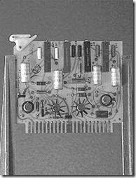
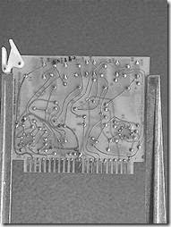
LEVEL I.—This level is normally associated with small modules or submodules that are attached to circuit cards or mother boards. The analog-to-digital (A/D) converter module is a device that converts a signal that is a function of a continuous variable (like a sine wave) into a representative number sequence in digital form. The A/D converter in figure 1-37 is a typical Level I component. At this level of

maintenance you can replace the faulty module with a good one. The faulty module can then be repaired at a later time or discarded. This concept significantly reduces the time equipment is inoperable.

clip_image005

Figure 1-37.—Printed circuit board (pcb).

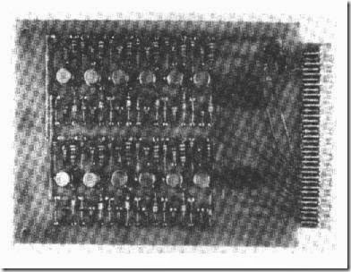
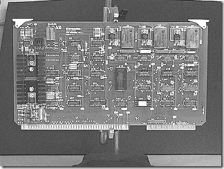
LEVEL II.—Level II packaging is composed of large printed circuit boards and/or cards (mother boards). Typical units of this level are shown in figures 1-37 and 1-38. In figure 1-38 the card measures 15 ´ 5.25 inches. The large dual inline packages (DIPs) are 2.25 inches x 0.75 inch. Other DIPs on the pcb are much smaller. Interconnections are shown between DIPs. You should also be able to locate a few discrete components. Repair consists of removing the faulty DIP or discrete component from the pcb and replacing it with a new part. Then the pcb is placed back into service. The removed part may be a level 0 or I part and would be handled as described in those sections. In some cases, the entire pcb should be replaced.

clip_image007

Figure 1-38.—Printed circuit board (pcb).

LEVEL III.—Drawers or pull-out chassis are level III units, as shown in figure 1-36. These are designed for accessibility and ease of maintenance. Normally, circuit cards associated with a particular subsystem will be grouped together in a drawer. This not only makes for an orderly arrangement of subsystems but also eliminates many long wiring harnesses. Defective cards are removed from such drawers and defective components are repaired as described in level II.

LEVEL IV.—Level IV is the highest level of packaging. It includes the cabinets, racks, and wiring harnesses necessary to interconnect all of the other levels. Other pieces of equipment of the same system classified as level IV, such as radar antennas, are broken down into levels 0 to III in the same manner.

During component troubleshooting procedures, you progress from level IV to III to II and on to level 0 where you identify the faulty component. As you become more familiar with a system, you should be able to go right to the drawer or module causing the problem.

Q40. Resistors, capacitors, transistors, and the like, are what level of packaging? Q41. Modules or submodules attached to a mother board are what packaging level? Q42. What is the packaging level of a pcb?