solid-state relay:,What It Does,Advantages,Disadvantages,How It Works,Variants,Instantaneous versus Zero Crossing,NC and NO Modes,Packaging,Solid-State Analog Switch,Values,How to Use It and What Can Go Wrong.

solid-state relay

A solid-state relay is less-commonly referred to by its acronym, SSR. It is sometimes regarded as an optocoupler, but in this encyclopedia the two components have separate entries. An optocoupler is a relatively simple device consisting of a light source (usually an LED) and a light sensor, in one package. It is used primarily for isolation rather than to switch a high current. A solid-state relay can be thought of as a substitute for an electromagnetic relay, usually has additional components in its package, and is intended to switch currents of at least 1A.

A component that works like a solid-state relay but only switches a 5V (or lower) logic signal may be referred to as a switch, even though it is entirely solid-state. This type of component is included in this entry because it functions so similarly to a solid-state relay.

What It Does

A solid-state relay (SSR) is a semiconductor package that emulates an electromagnetic re– lay (see Volume 1). It switches power on or off between its output terminals in response to a smaller current and voltage between its input terminals. Variants can switch AC or DC and may be controlled by AC or DC. An SSR functions as a SPST switch, and is available in normally open or normally closed versions. SSRs that function as an SPDT switch are relatively unusual and actual- ly contain more than one SSR.

No single schematic symbol has been adopted to represent a solid-state relay, but some alter- natives are shown in Figure 4-1:

Top

An unusually detailed depiction of an SSR that switches DC current using MOSFETS. Symbols for this device often omit the diodes

on the output side and may simplify the MOSFET symbols.

Bottom left

An SSR that uses an internal triac to switch

AC. The box labeled 0x indicates that this is a zero-crossing relay, meaning that it switches when alternating voltage crosses the 0V level from positive to negative or neg- ative to positive.

Bottom right

A generic SSR, showing a symbol for a nor- mally open relay, although whether it is de- signed for AC or DC is unclear.

Advantages

• Great reliability and long life.

• No physical contacts that are vulnerable to arcing and erosion or (under extreme con- ditions) that could weld themselves together.

• Very fast response, typically 1µs on and 0.5µs off.

• Very low power consumption on the input side, as low as 5mA at 5VDC. Many solid-state relays can be driven directly from logic chips.

• Lack of mechanical noise.

• No contact bounce; a clean output signal.

• No coil that would introduce back EMF into the circuit.

• Safe with flammable vapors, as there is no sparking of contacts.

• Often smaller than a comparable electro- magnetic relay.

• Insensitive to vibration.

• Safer for switching high voltages, as there is complete internal separation between input and output.

• Some variants work with input control vol- tages as low as 1.5VDC. Electromagnetic re- lays typically require at least 3VDC (or more, where larger relays are required to switch higher currents).

Disadvantages

• Less efficient; its internal impedance intro- duces a fixed-value voltage drop on the out- put side (although this may be negligible when switching higher voltages).

• Generates waste heat in its “on” mode, in ac- cordance with the voltage drop.

• Passes some leakage current (usually meas- ured in microamps) on the output side when the relay is supposed to be “off.”

• A DC solid-state relay usually requires obser- vation of polarity on the output side. An electromagnetic relay does not.

• Brief voltage spikes on the input side, which would be ignored by a slower electromag- netic relay, may trigger a solid-state relay.

• More vulnerable than an electromagnetic relay to surges and spikes in the current that is switched on the output side.

clip_image005

Figure 4-1. Schematic symbols for solid-state relays have not been standardized. See text for details.

How It Works

Almost all modern SSRs contain an internal LED (light-emitting diode, see Chapter 22) which is switched on by the control input. Infrared light from the LED is detected by a sensor consisting of one or more phototransistors or photodiodes. In a relay that controls DC current, the sensor usually switches a MOSFET (see Volume 1) or an SCR (silicon-controlled rectifier—see Chapter 1). In relays that control AC current, a triac (see Chapter 3) controls the output. Because the input side and the output side of the SSR are linked only by a light signal, they are electrically isolated from each other.

The MOSFETs require so little power, it can be provided entirely by light falling on an array of 20 or more photodiodes inside the SSR package.

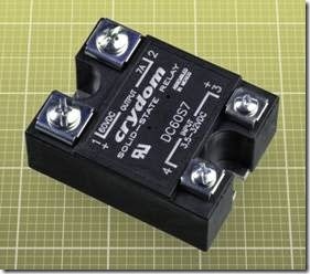
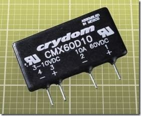
Typical solid-state relays are shown in Figures 4-2 and 4-3.

clip_image008

Figure 4-2. A solid-state relay capable of switching up to 7A DC. See text for a detailed description.

The Crydom DC60S7 accepts a control voltage ranging from 3.5VDC to 32VDC, with a typical in- put current of less than 3mA. Maximum turn-on time is 0.1ms and maximum turn-off time is 0.3ms. This relay can switch up to 7A and tolerates a surge of up to twice that current. It imposes a voltage drop of as much as 1.7VDC, which can become a drawback when switching voltages that are significantly lower than its maximum 60VDC. The electronics are sealed in thermally conductive epoxy, mounted on a metal plate ap- proximately 1/8” thick which can be screwed down onto an additional heat sink.

The Crydom CMX60D10 tolerates a more limited range of control voltages (3VDC to 10VDC) and requires a higher input current of 15mA at 5VDC. However, its very low maximum on-state resistance of 0.018Ω imposes a much smaller voltage drop of less than 0.2 volts when passing 10A. This results in less waste heat and enables a single- inline package (SIP) without a heat sink. The

CMX60D10 weighs 0.4 ounces, as opposed to the 3 ounces of the DC60S7. Relays from other manufacturers use similar packaging and have similar specifications.

clip_image010

Figure 4-3. A solid-state relay capable of switching up to 10A. Its lower internal resistance results in less waste heat and enables a smaller package. See text for a detailed description.

Variants

Many solid-state relays have protective components built into the package, such as a varistor on the output side to absorb transients. Check datasheets carefully to determine how much protection from external components may be necessary when switching an inductive load.

Instantaneous versus Zero Crossing

A zero crossing SSR is one that (a) switches AC current and (b) will not switch “on” until the instant when the AC voltage crosses through 0V. The advantages of this type are that it does not have to be built to switch such a high current, and creates minimal voltage spike when the switching occurs.

All SSRs that are designed to switch AC will wait for the next voltage zero crossing before switching to their “off” state.

NC and NO Modes

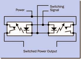
Solid-state relays are SPST devices, but different models may have a normally closed or normally open output. If you require double-throw operation, two relays can be combined, one normally closed, the other normally open. See Figure 4-4. A few manufacturers combine a normally closed relay and a normally open relay in one package, to emulate a SPDT relay.

clip_image013

Figure 4-4. A normally closed solid-state relay can be paired with a normally open solid-state relay to emulate a SPDT switch. This combination is available in a single package from some manufacturers.

Packaging

High-current solid-state relays are often pack- aged with screw terminals and a metal base that is appropriate for mating with a heat sink. Some are sold with heat sinks integrated. Spade terminals and crimp terminals may be optional. The Crydom DC60S7 shown in Figure 4-2 is an example. This type of package may be referred to as industrial mount.

Lower-current solid-state relays (5A or less), and those with a very low output resistance, may be packaged with single-inline pins for through- hole mounting in circuit boards.

Solid-State Analog Switch

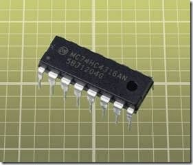
DIP packaging may be used for solid-state relays that are designed for compatibility with the low voltages and currents of logic chips. This type of component may be referred to simply as a switch. The 74HC4316 is an example, pictured in Figure 4-5.

clip_image015

Figure 4-5. This DIP package contains four “switches” that function as solid-state relays but are restricted to low voltages and currents, compatible with logic chips. See text for details.

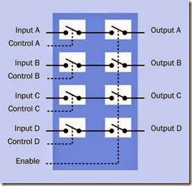
Typically the control voltage and the switched voltage are limited between +7V and −7V, with a maximum output current of 25mA. Each internal switch has its own Control pin, while an additional Enable pin forces all switches into an “off” state if its logic state is high. The simplified functionality of this component is illustrated in Figure 4-6, without showing internal optical isolation.

The “on” resistance of each internal pathway will be approximately 200Ω when the component is powered with +5VDC on the positive side and 0VDC on the negative side. This resistance drops to 100Ω if the negative power supply is -5VDC.

If all of the outputs from the chip are shorted together, it functions as a multiplexer (see Chap- ter 16). In fact, this type of switch component is often listed in catalogs as a multiplexer, even though it has other applications.

Because the component tolerates equal and opposite input voltages, it is capable of switching AC.

clip_image017

Figure 4-6. The functionality of a chip containing four solid-state analog switches. A high state on a Control pin closes its associated switch. The Enable pin must be held low for normal operation; a high Enable state forces all the switches into the “off” position. If the outputs are tied together, this component can function as a multiplexer.

Values

Industrial-mount solid-state relays typically can switch currents ranging from 5A to 500A, with 50A being very common. The higher-current re- lays mostly require DC control voltage; 4V to 32V are typical, although some versions can go much higher. They contain an SCR or triac to switch AC.

Smaller solid-state relays in SIP, DIP, or surface- mount packages often use MOSFETs on the out- put side, and are often capable of switching up to 2A or 3A. Some can switch either AC or DC, depending on the way the output is wired. The LED on the input side may require as little as 3mA to 5mA for triggering.

How to Use It

Solid-state relays find their primary uses in telecommunications equipment, industrial control systems and signalling, and security systems.

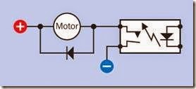
The component is very simple externally. Power on the input side can come from any source capable of delivering the voltage and current specified by the manufacturer, and any device that doesn’t exceed maximum current rating can be connected to the output side, so long as provision is made for suppressing back-EMF from an inductive load, as shown in Figure 4-7. Often a solid-state relay can be substituted directly for an electromagnetic relay, without modifying the circuit.

clip_image019

Figure 4-7. Use of a diode around an inductive load, to protect a solid-state relay from back-EMF.

Solid-state relays are heat sensitive, and their rating for switching current will diminish as their temperature increases. Manufacturer datasheets will provide specific guidance. Using a heat sink will greatly improve the performance. Bear in mind that the relay generates heat continuously while it is in its “on” mode—about 1 watt per ampere.

Because it requires so little current on the input side (typically no more than 15mA), a solid-state relay can usually be driven directly by chips such as microcontrollers that would not be able to ac- tivate an equivalent electromagnetic relay.

Applications may take advantage of the solid- state relay’s reliability, immunity to vibration, lack of contact sparking, freedom from coil- induced surges on the input side, and lack of contact bounce on the output side. A solid-state relay is ideal within digital equipment that is sensitive to power spikes. It may switch a fuel pump that handles volatile, flammable liquids, or a wastewater pump in a basement subject to flooding (where long-term zero-maintenance re- liability is necessary, and contact corrosion could be a risk in electromagnetic relays). Small solid- state relays can switch motors in robots or appliances where vibration is common, and are often used in arcade games.

What Can Go Wrong
Overheating Caused by Overloading

Relays must be derated when used at operating temperatures above the typical 20 or 25º C for which their specification applies. In other words, the sustained operating current must be reduced, usually by an amount such as 20% to 30% for each 10-degree increase in ambient temperature. Failure to observe this rule may result in failure of the component. Burnout may also occur if a high-current solid-state relay is used without a heat sink, or the heat sink isn’t big enough, or thermal compound is not applied be- tween the solid-state relay and the heat sink.

Overheating Caused by Bad Terminal Contact

If the screw terminals on the output side of a high-current solid-state relay are not tightened sufficiently, or if there is a loose spade terminal, or if a crimped connection isn’t crimped tightly enough, the poor contact will create electrical resistance, and at high currents, the resistance will create heat, which can cause the solid-state relay to overheat and burn out.

Overheating Caused by Changing Duty Cycle

If a high-current solid-state relay is chosen for an application where it is in its “on” state only half the time, but the application changes during product development so that the solid-state re- lay is in its “on” state almost all the time, it will have to dissippate almost twice as much heat. Any time the duty cycle is changed, heat should be considered. The possibility of the relay being used in an unconventional or unexpected manner should also be considered.

Overheating Caused by Component Crowding

Overheating increases dramatically when components are tightly crowded. At least 2cm (3/4”) should be allowed between components.

Overheating in Dual Packaging When a package contains two solid-state relays, the additive effects of the heat created by each of them must be considered.

Reverse-Voltage Burnout

Because a solid-state relay is more sensitive to back-EMF than an electromagnetic relay, greater care should be used to protect it from reverse voltage when switching inductive loads. A protection diode should be used, and a snubber can be added between its output terminals, if it is not included inside the relay package.

Low Voltage Output Current May Not Work

Unlike electromagnetic relays, solid-state relays require some voltage on the output side to en- able their internal operation. If there is no volt- age, or only a very low voltage, the SSR may not respond to an input. The minimum voltage required on the output side is usually specified in a datasheet.

To test a solid-state relay, apply actual voltages on input and output sides and use a load such as an incandescent light bulb. Merely applying a meter on the output side, set to measure continuity, may not provide sufficient voltage to en- able the relay to function, creating the erroneous impression that it has failed.

Inability to Measure AC Output When a multimeter is used to test continuity across the output of an AC-switching solid-state relay of zero-crossing specification, the meter

will generate enough voltage to prevent the solid-state relay from finding zero voltage across its output terminals, and consequently the solid- state relay won’t switch its output.

Relay Turns On but Won’t Turn Off When a solid-state relay controls a relatively high-impedance load such as a small solenoid

(see Volume 1) or a neon bulb (see Chapter 19), the relay may switch the device on but will seem unable to switch it off. This is because the leakage current of the solid-state relay, in its “off” state, may be just enough to maintain the load in its “on” state.

If an SSR containing a triac is used erroneously to switch DC, it will not be able to switch off the current.

Relays in Parallel Won’t Work

Two solid-state relays usually cannot be used in parallel to switch twice as much current. Because of small manufacturing variances, one relay will switch on a moment before the other. When the first relay is on, it will divert the load current away from the second relay. The second relay needs a small amount of current on its output side, to function. Without any current, it will not switch on. This means the first relay will pass the total current without any help from the second relay, and will probably burn out, while the second re- lay does nothing.

Output Device Doesn’t Run at Full Power

A solid-state relay imposes a voltage reduction on its output side. This will be a fixed amount, not a percentage. When switching 110V, this difference may be negligible; when switching 12V, it may deliver only 10.5V, which represents enough of a drop to cause a motor or a pump to run noticeably more slowly. The internal switching de- vice inside the relay (MOSFET, triac, SSR, or bipolar transistor) will largely determine the voltage drop. Check the manufacturer’s datasheet before using the relay.

Solid-State Relays and Safety Disconnects

Because a solid-state relay always allows some leakage in its “off” state, it can still deliver a shock when used to switch high voltages. For this reason, it may not be suitable in a safety disconnect.


triac:What It Does,Symbol Variants,How It Works,Quadrants,Threshold, Latching, and Holding Current,Triac Testing,Breakover Voltage,Switching AC,Triac Triggered by a Diac and Other Triac Drivers.

triac

A triac is a gate-triggered type of thyristor. Its name was probably derived from the phrase “triode for AC,” and because it is not an acronym, it is not usually capitalized.

A thyristor is defined here as a semiconductor having four or more layers of p-type and n-type silicon. Because the thyristor predated integrated circuits, and in its basic form consists of a single multilayer semiconductor, it is categorized as a discrete component in this encyclopedia. When a thyristor is combined with other components in one pack- age (as in a solid-state relay) it is considered to be an integrated circuit.

Other types of thyristor are the SCR (silicon-controlled rectifier) and the diac, each of which has its own entry in this encyclopedia.

Thyristor variants that are not so widely used, such as the gate turn-off thyristor (GTO) and silicon-controlled switch (SCS), do not have entries here.

What It Does

The triac is ubiquitous in AC dimmers for incandescent lamps. It is also used to control the speed of AC motors and the output of resistive heating elements. It is a type of thyristor which contains five segments of p-type and n-type silicon and has three leads, one of them attached to a gate that can switch a bidirectional flow of current between the other two. Its name was originally a trademark, generally thought to be derived from the phrase “triode for AC.” A triode was a common type of vacuum tube when thyristors were first introduced in the 1950s.

By comparison, a diac is a thyristor with only two leads, allowing current to flow in either direction when the component reaches a breakover volt- age. Its name was probably derived from the phrase “diode for AC.” It is often used in conjunction with a triac.

An SCR (silicon-controlled rectifier) is a thyristor that resembles a triac, as it has three leads, one of them a gate. However, it only allows current to flow in one direction.

Symbol Variants

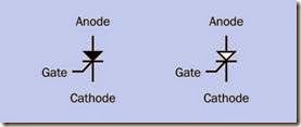
The schematic symbol for a triac, shown in Figure 3-1, resembles two diodes joined together, one of them inverted relative to the other. While a triac does not actually consist of two di- odes, it is functionally similar, and can pass cur- rent in either direction.

clip_image005

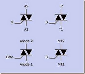
Figure 3-1. The schematic symbol for a triac, with four naming conventions that are used for its leads. The different conventions do not indicate any functional difference.

An appended bent line represents the gate. The labels for the other two leads are not standardized, and can be referred to as A1 and A2 (for Anode 1 and Anode 2), or T1 and T2 (for Terminal 1 and Terminal 2), or MT1 and MT2 (for Main Terminal 1 and Main Terminal 2). The choice of terms does not indicate any functional difference. In this encyclopedia entry, A1 and A2 are used.

The A1 terminal (or T1, or MT1) is always shown closer to the gate than A2 (or T2, or MT2). This distinction is important because although the triac can pass current in either direction, its behavior is somewhat asymmetrical.

• Voltages are expressed relative to terminal A1 (or T1, or MT1, if those terms are used).

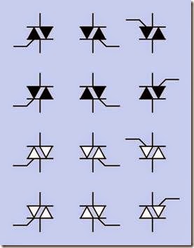
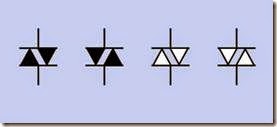
The schematic symbol may be reflected or rotated, the black triangles may have open centers, and the placement of the bent line representing the gate may vary. However, terminal A1 is always nearer to the gate than terminal A2.

Figure 3-2 shows 12 of the 16 theoretical possibilities. All of these variants are functionally identical. Occasionally the symbol has a circle around it, but this style is now rare.

clip_image007

Figure 3-2. Interchangeable variants of the schematic symbol for a triac.

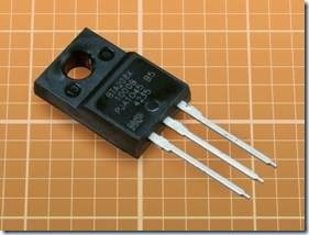
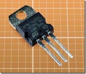
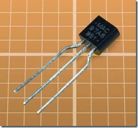
Triacs with various characteristics are shown in Figures 3-3, 3-4, and 3-5.

clip_image009

Figure 3-3. The BTA208X-1000B triac can conduct 8A continuous on-state current RMS, and withstands peak off-state voltage of up to 1,000V. This is a “snubberless” triac.

clip_image011

Figure 3-4. The BTB04-600SL triac can conduct 4A con- tinuous on-state current RMS, and withstands peak off- state voltage of up to 600V.

clip_image013

Figure 3-5. The MAC97A6 triac can conduct 0.8A contin- uous on-state current RMS, and withstands peak off-state voltage of up to 400V.

How It Works

When no gate voltage is applied, the triac remains in a passive state and will block current in either direction between A1 and A2, although a very small amount of leakage typically occurs. If the gate potential becomes sufficiently positive or negative relative to terminal A1, current can begin to flow between A1 and A2 in either direction. This makes the triac ideal for controlling AC.

Quadrants

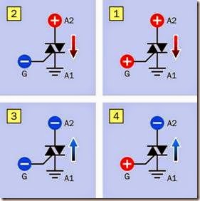
While a gate voltage is applied, four operating modes are possible. In each case, A1 is the reference (which can be thought of as being held at a neutral ground value). Because the triac is con- ducting AC, voltages above and below ground will occur. The four modes of operation are often referred to as four quadrants, and are typically arranged as shown in Figure 3-6.

In some reference sources (especially education- al text books), current is shown with an arrow indicating a flow of electrons moving from negative to positive. Because the type of current flow is often undefined, diagrams should be interpreted carefully. In this encyclopedia, current is always shown flowing from a more-positive location to a more-negative location.

Quadrant 1 (upper right)

A2 is more positive than A1, and the gate is more positive than A1. Conventional current (positive to negative) will flow from A2 to A1. (This behavior is very similar to that of an SCR.)

Quadrant 2 (upper left)

A2 is more positive than A1, and the gate is more negative than A1. Once again, conventional current (positive to negative) will flow from A2 to A1.

Quadrant 3 (lower left)

A2 is more negative than A1, and the gate is more negative than A1. Conventional cur- rent is reversed from A1 to A2.

Quadrant 4 (lower right)

A2 is more negative than A1, but the gate is more positive than A1. Conventional current is reversed from A1 to A2.

• Note that two positive symbols or two negative symbols in Figure 3-6 do not mean that both locations are of equal voltage. They simply mean that these

locations are at potentials that are sig- nificantly different from A1.

Threshold, Latching, and Holding Current

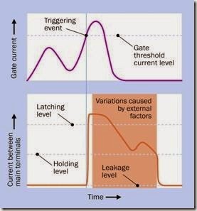
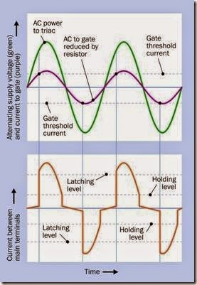
Figure 3-7 shows the relationship between the gate threshold current, the latching current, and holding current. In the upper half of the figure, gate current is shown fluctuating until it crosses the threshold level. This establishes current flow between the main terminals, shown in the lower half of the figure. Prior to this moment, a very small amount of leakage current occurred (shown in the figure, but not to scale).

In this hypothetical scenario, the triac starts passing current between external components—and the current exceeds the latching level. Consequently, gate current can diminish to zero, and the triac remains conductive. However, when external factors cause the current between the main terminals to diminish below the holding level, the triac abruptly ceases to be conductive, and current falls back to the leakage level.

clip_image016

Figure 3-6. The “quadrants” of triac behavior. Positive and negative symbols indicate which terminal is “more positive” or “more negative” than A1. The ground symbol represents a potential midway between positive and negative. See text for details.

Suppose that gate current increases gradually. When it reaches the gate threshold current of the triac, the component starts conducting between A1 and A2. If the current between A1 and A2 rises above the value known as the latching current, it will continue to flow, even if gate current disap-pears completely.

If the self-sustaining current through the triac gradually diminishes, while there is no voltage applied to the gate, conduction between the main terminals will stop spontaneously when it falls below a level known as the holding current. This behavior is similar to that of an SCR. The triac now returns to its original state, blocking current until the gate triggers it again.

The triac is sufficiently sensitive to respond to rapid fluctuations, as in 50Hz or 60Hz AC.

clip_image018

Figure 3-7. The relationship between gate current of a tri- ac and the current between its main terminals. See text for details.

Unlike a bipolar transistor, a triac is either “on” or “off” and does not function as a current amplifier. When it has been triggered, the impedance between A1 and A2 is low enough for heat dis- sipation to be manageable even at relatively high power levels.

Triac Testing

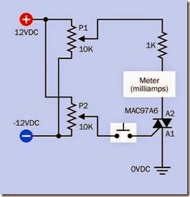
Figure 3-8 shows a circuit which can demonstrate the conductive behavior of a triac. For simplicity, this circuit is DC powered. In a real application, the triac is almost always used with AC.

clip_image020

Figure 3-8. A test circuit to show the behavior of a triac when varying positive and negative potentials are applied to the gate and to the A2 terminal, relative to A1.

Note that this circuit requires at least a +12VDC and -12VDC power supply (higher values may al- so be used). The ground symbol represents a midpoint voltage of 0VDC, applied to terminal A1 of the triac, which is an MAC97A6 or similar. If a dual-voltage power supply is unavailable, the gate of the triac can be connected directly to +12VDC, omitting potentiometer P2; but in this case, only two operating modes of the triac can be demonstrated by turning potentiometer P1.

Each potentiometer functions as a voltage divider between the positive and negative sides of the power supply. P1 applies a positive or negative voltage to A2, relative to A1. P2 applies a positive or negative voltage to the gate, relative to A1.

If the test begins with both potentiometers at the top ends of their range, A1 and G both have a positive potential relative to A1, so that the triac is now in quadrant 1 of its operating modes. Pressing the pushbutton should cause it to start conducting current limited by the 1K resistor, and the meter should change from measuring 0mA to around 12mA. If the pushbutton is re- leased, the triac should continue to conduct cur- rent, because 12mA is above this triac’s latching level. If P1 is slowly moved toward the center of its range, the current diminishes, ceasing when it falls below the holding level. If P1 is now moved back to the top of its range, the current will not resume until the triac is retriggered with the pushbutton.

The test can be repeated with P1 at the top of its range and P2 at the bottom of its range, to op- erate the triac in quadrant 2; P1 at the bottom of its range and P2 at the bottom of its range, to operate the triac in quadrant 3; and P1 at the bottom of its range and P2 at the top of its range, to operate the triac in quadrant 4. The function- ality should be the same in each case. The push- button will initiate a flow of current, which will diminish when P1 is turned toward the center of its range.

In any of these quadrants, P2 can be turned slowly toward the center of its range while the push- button is pressed repeatedly. This will allow empirical determination of the gate threshold cur- rent for this triac. The meter, measuring milliamps, will measure the current if it is inserted between the wiper of the potentiometer and the gate of the triac.

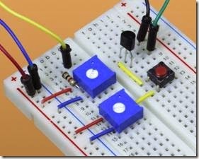
The test circuit is shown installed on a bread- board in Figure 3-9. In this photograph, the red and blue wires at left supply +12VDC and -12VDC relative to the black ground wire at top right. The yellow and green wires connect with a meter set to measure milliamps. The red button is a tactile switch, while the MAC97A6 triac is just above it

and to the left. The square blue 10K trimmers are set to opposite ends of their scales, so that the meter will show current flowing when the tactile switch is pressed.

clip_image022

Figure 3-9. A breadboarded triac test circuit.

Breakover Voltage

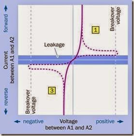
If a much higher voltage is applied to A2, the triac can be forced to conduct current without any triggering voltage being applied to the gate. This occurs when the potential between A1 and A2 reaches the triac’s breakover voltage, although the component is not designed to be used this way. The concept is illustrated in Figure 3-10, which can be compared with the behavior of an SCR illustrated in Figure 1-8 and the behavior of a diac shown in Figure 2-5. While the term break- down voltage defines the minimum reverse volt- age required to force a diode to conduct, break- over voltage refers to the minimum forward volt- age that has this effect. Because a triac is de- signed to conduct in both directions, it can be thought of as having a breakover voltage in both directions.
In Figure 3-10, the numbers in yellow squares are the quadrants referred to in Figure 3-6. The solid curve represents current flow if a triggering volt- age is applied to the gate while a positive or negative potential is applied to A2, relative to A1. If the gate is not triggered while the voltage between A1 and A2 gradually increases, the dashed section of the curve illustrates the outcome when the component reaches breakover voltage. Although this may not damage the triac, the component becomes uncontrollable.

• In normal usage, the voltage between A1 and A2 should not be allowed to reach break- over level.

clip_image024

Figure 3-10. The solid curve shows current passing be- tween A1 and A2 in a hypothetical triac, for varying voltages, while triggering voltage is applied to the gate. The dashed curve assumes that no triggering voltage is applied to the gate. The numbers in yellow squares are the quadrants of triac operation.

Switching AC

“Switching” AC with a triac means interrupting each pulse of current so that only a portion of it is conducted through to the load. Usually this is done with the triac functioning in quadrants 1 and 3. In quadrant 3, the polarity of the flow be- tween A1 and A2 is opposite to that in quadrant 1, and the gate voltage is also reversed. This enables a relatively simple circuit to control the duration of each half-cycle passing through the triac. The theory of this circuit is shown in Figure 3-11.

clip_image026

Figure 3-11. To moderate the power of AC current, a triac can block a section of each AC pulse.

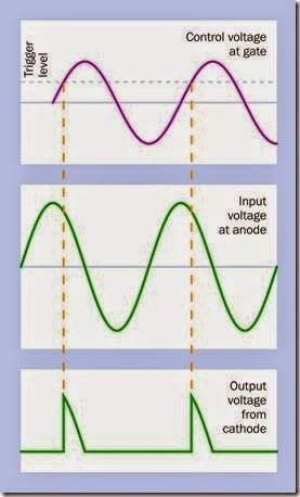
The upper section of Figure 3-11 shows alternating voltage to the triac in green. The purple curve represents the gate current of the triac, reduced by a variable resistor. (The figure is for conceptual purposes only; the alternating power supply voltage and the fluctuating gate current cannot actually share the same vertical scale of a graph.)

Figure 3-11 can be compared with Figure 3-7, except that the negative threshold level for the gate is now shown as well as the positive threshold level. Remember, either a positive or negative voltage can activate the gate.

In Figure 3-11, initially the triac is nonconductive. As time passes, the gate current reaches the threshold level, and this triggering event enables current to flow between the main terminals of the triac, as shown in the lower part of the figure.

This current exceeds the latching level, so it continues to flow, even though the gate current diminishes below its threshold level. Finally the current between the main terminals falls below the holding level, at which point the triac stops conducting. It waits for the next triggering event, which occurs as the power supply swings to negative.

This simple system blocks a section of each AC pulse, which will vary in length depending how much current is allowed to flow through the gate. Because the blocking process occurs rapidly, we notice only the reduced overall power passing through the triac (in terms of the brightness of a light, the heat emitted by a resistive element, or the speed of a motor).

Unfortunately, there is a problem in this scenario: the triac does not quite behave symmetrically. Its gate threshold level for positive current is not exactly equal and opposite to its gate threshold level for negative current. The upper part of Figure 3-11 shows this flaw in the differing vertical offsets of the positive and negative thresh- olds from the central zero line.

The result is that negative AC pulses through the triac are shorter than positive pulses. This asym- metry produces harmonics and noise that can feed back into power supply wiring, interfering with other electronic equipment. The actual dis- parities in gate response, in each quadrant of operation for two triacs, are shown in Figure 3-12.

clip_image028

Figure 3-12. Because the internal structure of a triac is asymmetrical, it requires a different trigger current in each of its operating quadrants. This table, derived from a Littelfuse technical briefing document, shows the ratio of the minimum trigger current in quadrants 2, 3, and 4 relative to quadrant 1.

See Figure 1-14 for a graph illustrating phase control in the SCR. See “Phase Control” for a dis- cussion of phase in AC waveforms generally.

Triac Triggered by a Diac

The problem of asymmetrical triggering can be overcome if the triac is triggered with a voltage pulse generated by another component that does behave symmetrically. The other component is almost always a diac, which is another type of thyristor. Unlike an SCR or a triac, it has no gate. It is designed to be pushed beyond its breakover voltage, at which point it latches and will continue to conduct until current flowing through it diminishes below its holding level. See Chapter 2 for more information about the diac.

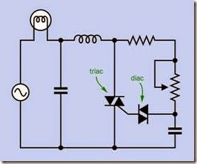
In Figure 3-13, the diac is shown to the right of the triac, and is driven by a simple RC network consisting of a fixed resistor, a potentiometer, and a capacitor. (In an actual application, the RC network may be slightly more complex.) The ca- pacitor takes a small amount of time to charge during each half-cycle of AC. The length of this delay is adjusted by the potentiometer, and de- termines the point in each AC half-cycle when the voltage to the diac reaches breakover level. Because the delay affects the phase of the AC, this adjustment is known as phase control.

As the voltage exceeds breakover level, the diac starts to pass current through to the gate of the triac, and triggers it. The holding level of the diac is lower than its latching level, so it continues to pass current while the capacitor discharges and the voltage diminishes. When the current falls below the holding level, the diac stops conduct- ing, ready for the next cycle. Meanwhile, the triac continues to pass current until the AC voltage dips below its holding level. At this point, the triac becomes nonconductive until it is triggered again.

This chopped waveform will still create some harmonics, which are suppressed by the coil and capacitor at the left side of the circuit in Figure 3-13.

clip_image030

Figure 3-13. A minimal schematic showing typical opera- tion of a triac, with a diac supplying pulses to the triac gate. The potentiometer adjusts the delay created by the capacitor.

Other Triac Drivers

It is possible, although unusual, to drive a triac from a source other than a diac.

Simple on-off control can be achieved by using a special optocoupler such as the MOC3162 by Fairchild Semiconductor. This emits a switching signal to a triac only when the AC voltage passes through zero. A zero cross circuit is desirable be- cause it creates much less interference. The use of an optocoupler helps to isolate the triac from other components.(((“zero cross circuit”))

Phase control can be achieved using an opto- coupler such as the H11L1, which can be driven by rectified but unsmoothed AC after it passes through a Zener diode to limit the voltage. The output from the optocoupler is logic-compatible and can be connected with the input to a timer such as the 555, set to one-shot mode. Each pulse from the timer passes through another optocou- pler such as the MOC3023, which uses an internal LED to trigger the gate of a triac.

Yet another possibility is to use the programmed output from a microcontroller, through an opto- coupler, to control the gate of a triac. An online search for the terms “microcontroller” and “triac” will provide some additional suggestions.

Charge Storage

While switching AC, the internal charge between A1 and A2 inside the triac requires time to dissipate before the reverse voltage is applied; other- wise, charge storage occurs, and the component may start to conduct continuously. For this reason, the triac is normally restricted to relatively low frequencies such as domestic 60Hz AC power.

When a triac controls a motor, the phase lag be- tween voltage and current associated with an inductive load can interfere with the triac’s need for a transitional moment between a positive and negative voltage cycle. In a datasheet, the term commutating dv/dt defines the rate of rise of opposite polarity voltage that the triac can with- stand without locking into a continuous-on state.

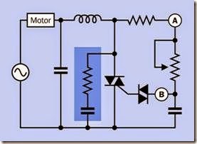
An RC snubber network is often wired in parallel with A1 and A2 to control the rise time of voltage to the triac, as shown within the darker blue rec- tangle in Figure 3-14, where a resistor and ca- pacitor have been added just to the left of the triac. The highest resistance and lowest capaci- tance, consistent with trouble-free operation, should be chosen. Typical values are 47Ω to 100Ω for the resistor, and 0.01µF to 0.1µF for the capacitor.

Variants

clip_image032

Figure 3-14. To prevent a triac from locking itself into a continuous-on state while driving an inductive load such as a motor, a snubber circuit can be added (shown here as a resistor and capacitor in the darker blue rectangle to the left of the triac).

A snubberless triac, as its name implies, is de- signed to drive an inductive load without need for a snubber circuit. An example is the STMicroelectronics BTA24. Datasheets for this type of component impose some limits that may be stricter than for a generic triac.

Values

Surface-mount triacs are typically rated between 2A to 25A of switched AC current (RMS), the higher-current versions being as large as 10mm square. The necessary gate trigger voltage may range from 0.7V to 1.5V. Through-hole packages may be capable of slightly higher currents (up to 40A), with gate trigger voltages of 1V to 2.5V being common.

Triacs are available in through-hole and surface- mount packages.

Some components that are referred to as triacs actually contain two SCR components of opposite polarity. The “alternistor” range from Littel- fuse is an example. The SCR will tolerate faster voltage rise times than a conventional triac, and is more suitable for driving inductive loads such as large motors.

As noted previously, the majority of triacs are restricted to relatively low frequency switching, 60Hz being very common.

Abbreviations in datasheets are likely to include:

• VDRM or VRRM Peak repetitive reverse off-state voltage. The maximum reverse voltage that the component will withstand in its “off” state without experiencing damage or al- lowing current to pass.

• VTM The maximum voltage difference be- tween A1 and A2, measured with a short pulse width and low duty cycle.

• VGT Gate trigger voltage necessary to pro- duce the gate trigger current.

• IDRM Peak repetitive blocking current (i.e., maximum leakage).

• IGM Maximum gate current.

• IGT Minimum gate trigger current.

• IH Holding current.

• IL Latching current.

• IT(RMS) On-state RMS current. The maximum value passing through the component on a continuous basis.

• ITSM Maximum non-repetitive surge current. Specified at a stated pulse width, usually 60 Hz.

• TC Case temperature, usually expressed as an acceptable range.

• TJ Operating junction temperature, usually expressed as an acceptable range.

What Can Go Wrong

Like other semiconductors, a triac is heat sensi- tive. Usual precautions should be taken to allow sufficient ventilation and heat sinking, especially when components are moved from an open pro- totyping board to an enclosure in which crowd- ing is likely.

Unexpected Triggering Caused by Heat

On a datasheet, a value for triggering current is valid only within a recommended temperature range. A buildup of heat can provoke unexpec- ted triggering.

Low-Temperature Effects

Significantly higher gate current will be required by a triac operating at low temperatures. It is quite possible that the component will need twice as much current at 25º C compared with 100º C, junction temperature. If the triac receives insufficient current, it will not turn on.

Wrong Type of Load

If an incandescent lamp is replaced with a flu- orescent light or LED area lighting, a pre- existing triac may no longer work as a dimmer. Fluorescent lamps will have some inductance, and may also provide a capacitive load, either of which will interfere with the normal behavior of a triac.

The light output of an LED varies very differently compared with the light output of an incandescent bulb, in response to reduction in power. Therefore an LED should be dimmed using pulse- width modulation that is appropriate for its out- put characteristics. A triac is generally not suitable.

Wrongly Identified Terminals

A triac is often thought of as a symmetrical de- vice, because it is designed to switch AC current using either positive or negative voltage at the gate. In reality, its behavior is asymmetrical, and if it is installed “the wrong way around” it may function erratically or not at all.

Failure to Switch Off

As already noted (see “Charge Storage” on page 23), a triac will tend to suffer from charge stor- age if there is insufficient time between the end of one half-cycle and the beginning of the next. A component that works with a resistive load may cease to function if it is used, instead, to power an inductive load.


triac:What It Does,Symbol Variants,How It Works,Quadrants,Threshold, Latching, and Holding Current,Triac Testing,Breakover Voltage,Switching AC,Triac Triggered by a Diac and Other Triac Drivers.

triac

A triac is a gate-triggered type of thyristor. Its name was probably derived from the phrase “triode for AC,” and because it is not an acronym, it is not usually capitalized.

A thyristor is defined here as a semiconductor having four or more layers of p-type and n-type silicon. Because the thyristor predated integrated circuits, and in its basic form consists of a single multilayer semiconductor, it is categorized as a discrete component in this encyclopedia. When a thyristor is combined with other components in one pack- age (as in a solid-state relay) it is considered to be an integrated circuit.

Other types of thyristor are the SCR (silicon-controlled rectifier) and the diac, each of which has its own entry in this encyclopedia.

Thyristor variants that are not so widely used, such as the gate turn-off thyristor (GTO) and silicon-controlled switch (SCS), do not have entries here.

What It Does

The triac is ubiquitous in AC dimmers for incandescent lamps. It is also used to control the speed of AC motors and the output of resistive heating elements. It is a type of thyristor which contains five segments of p-type and n-type silicon and has three leads, one of them attached to a gate that can switch a bidirectional flow of current between the other two. Its name was originally a trademark, generally thought to be derived from the phrase “triode for AC.” A triode was a common type of vacuum tube when thyristors were first introduced in the 1950s.

By comparison, a diac is a thyristor with only two leads, allowing current to flow in either direction when the component reaches a breakover volt- age. Its name was probably derived from the phrase “diode for AC.” It is often used in conjunction with a triac.

An SCR (silicon-controlled rectifier) is a thyristor that resembles a triac, as it has three leads, one of them a gate. However, it only allows current to flow in one direction.

Symbol Variants

The schematic symbol for a triac, shown in Figure 3-1, resembles two diodes joined together, one of them inverted relative to the other. While a triac does not actually consist of two di- odes, it is functionally similar, and can pass cur- rent in either direction.

clip_image005

Figure 3-1. The schematic symbol for a triac, with four naming conventions that are used for its leads. The different conventions do not indicate any functional difference.

An appended bent line represents the gate. The labels for the other two leads are not standardized, and can be referred to as A1 and A2 (for Anode 1 and Anode 2), or T1 and T2 (for Terminal 1 and Terminal 2), or MT1 and MT2 (for Main Terminal 1 and Main Terminal 2). The choice of terms does not indicate any functional difference. In this encyclopedia entry, A1 and A2 are used.

The A1 terminal (or T1, or MT1) is always shown closer to the gate than A2 (or T2, or MT2). This distinction is important because although the triac can pass current in either direction, its behavior is somewhat asymmetrical.

• Voltages are expressed relative to terminal A1 (or T1, or MT1, if those terms are used).

The schematic symbol may be reflected or rotated, the black triangles may have open centers, and the placement of the bent line representing the gate may vary. However, terminal A1 is always nearer to the gate than terminal A2.

Figure 3-2 shows 12 of the 16 theoretical possibilities. All of these variants are functionally identical. Occasionally the symbol has a circle around it, but this style is now rare.

clip_image007

Figure 3-2. Interchangeable variants of the schematic symbol for a triac.

Triacs with various characteristics are shown in Figures 3-3, 3-4, and 3-5.

clip_image009

Figure 3-3. The BTA208X-1000B triac can conduct 8A continuous on-state current RMS, and withstands peak off-state voltage of up to 1,000V. This is a “snubberless” triac.

clip_image011

Figure 3-4. The BTB04-600SL triac can conduct 4A con- tinuous on-state current RMS, and withstands peak off- state voltage of up to 600V.

clip_image013

Figure 3-5. The MAC97A6 triac can conduct 0.8A contin- uous on-state current RMS, and withstands peak off-state voltage of up to 400V.

How It Works

When no gate voltage is applied, the triac remains in a passive state and will block current in either direction between A1 and A2, although a very small amount of leakage typically occurs. If the gate potential becomes sufficiently positive or negative relative to terminal A1, current can begin to flow between A1 and A2 in either direction. This makes the triac ideal for controlling AC.

Quadrants

While a gate voltage is applied, four operating modes are possible. In each case, A1 is the reference (which can be thought of as being held at a neutral ground value). Because the triac is con- ducting AC, voltages above and below ground will occur. The four modes of operation are often referred to as four quadrants, and are typically arranged as shown in Figure 3-6.

In some reference sources (especially education- al text books), current is shown with an arrow indicating a flow of electrons moving from negative to positive. Because the type of current flow is often undefined, diagrams should be interpreted carefully. In this encyclopedia, current is always shown flowing from a more-positive location to a more-negative location.

Quadrant 1 (upper right)

A2 is more positive than A1, and the gate is more positive than A1. Conventional current (positive to negative) will flow from A2 to A1. (This behavior is very similar to that of an SCR.)

Quadrant 2 (upper left)

A2 is more positive than A1, and the gate is more negative than A1. Once again, conventional current (positive to negative) will flow from A2 to A1.

Quadrant 3 (lower left)

A2 is more negative than A1, and the gate is more negative than A1. Conventional cur- rent is reversed from A1 to A2.

Quadrant 4 (lower right)

A2 is more negative than A1, but the gate is more positive than A1. Conventional current is reversed from A1 to A2.

• Note that two positive symbols or two negative symbols in Figure 3-6 do not mean that both locations are of equal voltage. They simply mean that these

locations are at potentials that are sig- nificantly different from A1.

Threshold, Latching, and Holding Current

Figure 3-7 shows the relationship between the gate threshold current, the latching current, and holding current. In the upper half of the figure, gate current is shown fluctuating until it crosses the threshold level. This establishes current flow between the main terminals, shown in the lower half of the figure. Prior to this moment, a very small amount of leakage current occurred (shown in the figure, but not to scale).

In this hypothetical scenario, the triac starts passing current between external components—and the current exceeds the latching level. Consequently, gate current can diminish to zero, and the triac remains conductive. However, when external factors cause the current between the main terminals to diminish below the holding level, the triac abruptly ceases to be conductive, and current falls back to the leakage level.

clip_image016

Figure 3-6. The “quadrants” of triac behavior. Positive and negative symbols indicate which terminal is “more positive” or “more negative” than A1. The ground symbol represents a potential midway between positive and negative. See text for details.

Suppose that gate current increases gradually. When it reaches the gate threshold current of the triac, the component starts conducting between A1 and A2. If the current between A1 and A2 rises above the value known as the latching current, it will continue to flow, even if gate current disap-pears completely.

If the self-sustaining current through the triac gradually diminishes, while there is no voltage applied to the gate, conduction between the main terminals will stop spontaneously when it falls below a level known as the holding current. This behavior is similar to that of an SCR. The triac now returns to its original state, blocking current until the gate triggers it again.

The triac is sufficiently sensitive to respond to rapid fluctuations, as in 50Hz or 60Hz AC.

clip_image018

Figure 3-7. The relationship between gate current of a tri- ac and the current between its main terminals. See text for details.

Unlike a bipolar transistor, a triac is either “on” or “off” and does not function as a current amplifier. When it has been triggered, the impedance between A1 and A2 is low enough for heat dis- sipation to be manageable even at relatively high power levels.

Triac Testing

Figure 3-8 shows a circuit which can demonstrate the conductive behavior of a triac. For simplicity, this circuit is DC powered. In a real application, the triac is almost always used with AC.

clip_image020

Figure 3-8. A test circuit to show the behavior of a triac when varying positive and negative potentials are applied to the gate and to the A2 terminal, relative to A1.

Note that this circuit requires at least a +12VDC and -12VDC power supply (higher values may al- so be used). The ground symbol represents a midpoint voltage of 0VDC, applied to terminal A1 of the triac, which is an MAC97A6 or similar. If a dual-voltage power supply is unavailable, the gate of the triac can be connected directly to +12VDC, omitting potentiometer P2; but in this case, only two operating modes of the triac can be demonstrated by turning potentiometer P1.

Each potentiometer functions as a voltage divider between the positive and negative sides of the power supply. P1 applies a positive or negative voltage to A2, relative to A1. P2 applies a positive or negative voltage to the gate, relative to A1.

If the test begins with both potentiometers at the top ends of their range, A1 and G both have a positive potential relative to A1, so that the triac is now in quadrant 1 of its operating modes. Pressing the pushbutton should cause it to start conducting current limited by the 1K resistor, and the meter should change from measuring 0mA to around 12mA. If the pushbutton is re- leased, the triac should continue to conduct cur- rent, because 12mA is above this triac’s latching level. If P1 is slowly moved toward the center of its range, the current diminishes, ceasing when it falls below the holding level. If P1 is now moved back to the top of its range, the current will not resume until the triac is retriggered with the pushbutton.

The test can be repeated with P1 at the top of its range and P2 at the bottom of its range, to op- erate the triac in quadrant 2; P1 at the bottom of its range and P2 at the bottom of its range, to operate the triac in quadrant 3; and P1 at the bottom of its range and P2 at the top of its range, to operate the triac in quadrant 4. The function- ality should be the same in each case. The push- button will initiate a flow of current, which will diminish when P1 is turned toward the center of its range.

In any of these quadrants, P2 can be turned slowly toward the center of its range while the push- button is pressed repeatedly. This will allow empirical determination of the gate threshold cur- rent for this triac. The meter, measuring milliamps, will measure the current if it is inserted between the wiper of the potentiometer and the gate of the triac.

The test circuit is shown installed on a bread- board in Figure 3-9. In this photograph, the red and blue wires at left supply +12VDC and -12VDC relative to the black ground wire at top right. The yellow and green wires connect with a meter set to measure milliamps. The red button is a tactile switch, while the MAC97A6 triac is just above it

and to the left. The square blue 10K trimmers are set to opposite ends of their scales, so that the meter will show current flowing when the tactile switch is pressed.

clip_image022

Figure 3-9. A breadboarded triac test circuit.

Breakover Voltage

If a much higher voltage is applied to A2, the triac can be forced to conduct current without any triggering voltage being applied to the gate. This occurs when the potential between A1 and A2 reaches the triac’s breakover voltage, although the component is not designed to be used this way. The concept is illustrated in Figure 3-10, which can be compared with the behavior of an SCR illustrated in Figure 1-8 and the behavior of a diac shown in Figure 2-5. While the term break- down voltage defines the minimum reverse volt- age required to force a diode to conduct, break- over voltage refers to the minimum forward volt- age that has this effect. Because a triac is de- signed to conduct in both directions, it can be thought of as having a breakover voltage in both directions.
In Figure 3-10, the numbers in yellow squares are the quadrants referred to in Figure 3-6. The solid curve represents current flow if a triggering volt- age is applied to the gate while a positive or negative potential is applied to A2, relative to A1. If the gate is not triggered while the voltage between A1 and A2 gradually increases, the dashed section of the curve illustrates the outcome when the component reaches breakover voltage. Although this may not damage the triac, the component becomes uncontrollable.

• In normal usage, the voltage between A1 and A2 should not be allowed to reach break- over level.

clip_image024

Figure 3-10. The solid curve shows current passing be- tween A1 and A2 in a hypothetical triac, for varying voltages, while triggering voltage is applied to the gate. The dashed curve assumes that no triggering voltage is applied to the gate. The numbers in yellow squares are the quadrants of triac operation.

Switching AC

“Switching” AC with a triac means interrupting each pulse of current so that only a portion of it is conducted through to the load. Usually this is done with the triac functioning in quadrants 1 and 3. In quadrant 3, the polarity of the flow be- tween A1 and A2 is opposite to that in quadrant 1, and the gate voltage is also reversed. This enables a relatively simple circuit to control the duration of each half-cycle passing through the triac. The theory of this circuit is shown in Figure 3-11.

clip_image026

Figure 3-11. To moderate the power of AC current, a triac can block a section of each AC pulse.

The upper section of Figure 3-11 shows alternating voltage to the triac in green. The purple curve represents the gate current of the triac, reduced by a variable resistor. (The figure is for conceptual purposes only; the alternating power supply voltage and the fluctuating gate current cannot actually share the same vertical scale of a graph.)

Figure 3-11 can be compared with Figure 3-7, except that the negative threshold level for the gate is now shown as well as the positive threshold level. Remember, either a positive or negative voltage can activate the gate.

In Figure 3-11, initially the triac is nonconductive. As time passes, the gate current reaches the threshold level, and this triggering event enables current to flow between the main terminals of the triac, as shown in the lower part of the figure.

This current exceeds the latching level, so it continues to flow, even though the gate current diminishes below its threshold level. Finally the current between the main terminals falls below the holding level, at which point the triac stops conducting. It waits for the next triggering event, which occurs as the power supply swings to negative.

This simple system blocks a section of each AC pulse, which will vary in length depending how much current is allowed to flow through the gate. Because the blocking process occurs rapidly, we notice only the reduced overall power passing through the triac (in terms of the brightness of a light, the heat emitted by a resistive element, or the speed of a motor).

Unfortunately, there is a problem in this scenario: the triac does not quite behave symmetrically. Its gate threshold level for positive current is not exactly equal and opposite to its gate threshold level for negative current. The upper part of Figure 3-11 shows this flaw in the differing vertical offsets of the positive and negative thresh- olds from the central zero line.
The result is that negative AC pulses through the triac are shorter than positive pulses. This asym- metry produces harmonics and noise that can feed back into power supply wiring, interfering with other electronic equipment. The actual dis- parities in gate response, in each quadrant of operation for two triacs, are shown in Figure 3-12.

clip_image028

Figure 3-12. Because the internal structure of a triac is asymmetrical, it requires a different trigger current in each of its operating quadrants. This table, derived from a Littelfuse technical briefing document, shows the ratio of the minimum trigger current in quadrants 2, 3, and 4 relative to quadrant 1.

See Figure 1-14 for a graph illustrating phase control in the SCR. See “Phase Control” for a dis- cussion of phase in AC waveforms generally.

Triac Triggered by a Diac

The problem of asymmetrical triggering can be overcome if the triac is triggered with a voltage pulse generated by another component that does behave symmetrically. The other component is almost always a diac, which is another type of thyristor. Unlike an SCR or a triac, it has no gate. It is designed to be pushed beyond its breakover voltage, at which point it latches and will continue to conduct until current flowing through it diminishes below its holding level. See Chapter 2 for more information about the diac.

In Figure 3-13, the diac is shown to the right of the triac, and is driven by a simple RC network consisting of a fixed resistor, a potentiometer, and a capacitor. (In an actual application, the RC network may be slightly more complex.) The ca- pacitor takes a small amount of time to charge during each half-cycle of AC. The length of this delay is adjusted by the potentiometer, and de- termines the point in each AC half-cycle when the voltage to the diac reaches breakover level. Because the delay affects the phase of the AC, this adjustment is known as phase control.

As the voltage exceeds breakover level, the diac starts to pass current through to the gate of the triac, and triggers it. The holding level of the diac is lower than its latching level, so it continues to pass current while the capacitor discharges and the voltage diminishes. When the current falls below the holding level, the diac stops conduct- ing, ready for the next cycle. Meanwhile, the triac continues to pass current until the AC voltage dips below its holding level. At this point, the triac becomes nonconductive until it is triggered again.

This chopped waveform will still create some harmonics, which are suppressed by the coil and capacitor at the left side of the circuit in Figure 3-13.

clip_image030

Figure 3-13. A minimal schematic showing typical opera- tion of a triac, with a diac supplying pulses to the triac gate. The potentiometer adjusts the delay created by the capacitor.

Other Triac Drivers

It is possible, although unusual, to drive a triac from a source other than a diac.

Simple on-off control can be achieved by using a special optocoupler such as the MOC3162 by Fairchild Semiconductor. This emits a switching signal to a triac only when the AC voltage passes through zero. A zero cross circuit is desirable be- cause it creates much less interference. The use of an optocoupler helps to isolate the triac from other components.(((“zero cross circuit”))

Phase control can be achieved using an opto- coupler such as the H11L1, which can be driven by rectified but unsmoothed AC after it passes through a Zener diode to limit the voltage. The output from the optocoupler is logic-compatible and can be connected with the input to a timer such as the 555, set to one-shot mode. Each pulse from the timer passes through another optocou- pler such as the MOC3023, which uses an internal LED to trigger the gate of a triac.

Yet another possibility is to use the programmed output from a microcontroller, through an opto- coupler, to control the gate of a triac. An online search for the terms “microcontroller” and “triac” will provide some additional suggestions.

Charge Storage

While switching AC, the internal charge between A1 and A2 inside the triac requires time to dissipate before the reverse voltage is applied; other- wise, charge storage occurs, and the component may start to conduct continuously. For this reason, the triac is normally restricted to relatively low frequencies such as domestic 60Hz AC power.

When a triac controls a motor, the phase lag be- tween voltage and current associated with an inductive load can interfere with the triac’s need for a transitional moment between a positive and negative voltage cycle. In a datasheet, the term commutating dv/dt defines the rate of rise of opposite polarity voltage that the triac can with- stand without locking into a continuous-on state.

An RC snubber network is often wired in parallel with A1 and A2 to control the rise time of voltage to the triac, as shown within the darker blue rec- tangle in Figure 3-14, where a resistor and ca- pacitor have been added just to the left of the triac. The highest resistance and lowest capaci- tance, consistent with trouble-free operation, should be chosen. Typical values are 47Ω to 100Ω for the resistor, and 0.01µF to 0.1µF for the capacitor.

Variants

clip_image032

Figure 3-14. To prevent a triac from locking itself into a continuous-on state while driving an inductive load such as a motor, a snubber circuit can be added (shown here as a resistor and capacitor in the darker blue rectangle to the left of the triac).

A snubberless triac, as its name implies, is de- signed to drive an inductive load without need for a snubber circuit. An example is the STMicroelectronics BTA24. Datasheets for this type of component impose some limits that may be stricter than for a generic triac.

Values

Surface-mount triacs are typically rated between 2A to 25A of switched AC current (RMS), the higher-current versions being as large as 10mm square. The necessary gate trigger voltage may range from 0.7V to 1.5V. Through-hole packages may be capable of slightly higher currents (up to 40A), with gate trigger voltages of 1V to 2.5V being common.

Triacs are available in through-hole and surface- mount packages.

Some components that are referred to as triacs actually contain two SCR components of opposite polarity. The “alternistor” range from Littel- fuse is an example. The SCR will tolerate faster voltage rise times than a conventional triac, and is more suitable for driving inductive loads such as large motors.

As noted previously, the majority of triacs are restricted to relatively low frequency switching, 60Hz being very common.

Abbreviations in datasheets are likely to include:

• VDRM or VRRM Peak repetitive reverse off-state voltage. The maximum reverse voltage that the component will withstand in its “off” state without experiencing damage or al- lowing current to pass.

• VTM The maximum voltage difference be- tween A1 and A2, measured with a short pulse width and low duty cycle.

• VGT Gate trigger voltage necessary to pro- duce the gate trigger current.

• IDRM Peak repetitive blocking current (i.e., maximum leakage).

• IGM Maximum gate current.

• IGT Minimum gate trigger current.

• IH Holding current.

• IL Latching current.

• IT(RMS) On-state RMS current. The maximum value passing through the component on a continuous basis.

• ITSM Maximum non-repetitive surge current. Specified at a stated pulse width, usually 60 Hz.

• TC Case temperature, usually expressed as an acceptable range.

• TJ Operating junction temperature, usually expressed as an acceptable range.

What Can Go Wrong

Like other semiconductors, a triac is heat sensi- tive. Usual precautions should be taken to allow sufficient ventilation and heat sinking, especially when components are moved from an open pro- totyping board to an enclosure in which crowd- ing is likely.

Unexpected Triggering Caused by Heat

On a datasheet, a value for triggering current is valid only within a recommended temperature range. A buildup of heat can provoke unexpec- ted triggering.

Low-Temperature Effects

Significantly higher gate current will be required by a triac operating at low temperatures. It is quite possible that the component will need twice as much current at 25º C compared with 100º C, junction temperature. If the triac receives insufficient current, it will not turn on.

Wrong Type of Load

If an incandescent lamp is replaced with a flu- orescent light or LED area lighting, a pre- existing triac may no longer work as a dimmer. Fluorescent lamps will have some inductance, and may also provide a capacitive load, either of which will interfere with the normal behavior of a triac.

The light output of an LED varies very differently compared with the light output of an incandescent bulb, in response to reduction in power. Therefore an LED should be dimmed using pulse- width modulation that is appropriate for its out- put characteristics. A triac is generally not suitable.

Wrongly Identified Terminals

A triac is often thought of as a symmetrical de- vice, because it is designed to switch AC current using either positive or negative voltage at the gate. In reality, its behavior is asymmetrical, and if it is installed “the wrong way around” it may function erratically or not at all.

Failure to Switch Off

As already noted (see “Charge Storage” on page 23), a triac will tend to suffer from charge stor- age if there is insufficient time between the end of one half-cycle and the beginning of the next. A component that works with a resistive load may cease to function if it is used, instead, to power an inductive load.


SCR:What It Does,How It Works,Switching Behavior,Internal Configuration,Breakdown and Breakover Voltage,SCR Concept Demoand AC Current Applications.

SCR

The acronym SCR is derived from silicon-controlled rectifier, which is a gate-triggered type of thyristor. A thyristor is defined here as a semiconductor having four or more alternating layers of p-type and n-type silicon. Because it predated integrated circuits, and in its basic form consists of a single multilayer semiconductor, a thyristor is considered to be a discrete component in this encyclopedia. When a thyristor is combined with other components in one package (as in a solid-state relay), it is considered to be an integrated circuit.

Other types of thyristor are the diac and triac, each of which has its own entry. Thyristor variants that are not so widely used, such as the gate turn-off thyristor (GTO) and silicon-controlled switch (SCS), do not have entries here.

What It Does

In the 1920s, the thyratron was a gas-filled tube that functioned as a switch and a rectifier. In 1956, General Electric introduced a solid-state version of it under the name thyristor. In both cases, the names were derived from the thyroid gland in the human body, which controls the rate of consumption of energy. The thyratron and, subsequently, the thyristor enabled control of large flows of current.

The SCR (silicon-controlled rectifier) is a type of thyristor, although the two terms are often used as if they are synonymous. Text that refers loosely to a thyristor may actually be discussing an SCR, and vice versa. In this encyclopedia, the SCR, di- ac, and triac are all considered to be variant types of thyristor.

An SCR is a solid-state switch that in many in- stances can pass high currents at high voltages.

Like a bipolar transistor, it is triggered by volt- age applied to a gate. Unlike the transistor, it al- lows the flow of current to continue even when the gate voltage diminishes to zero.

How It Works

This component is designed to pass current in one direction only. It can be forced to conduct in the opposite direction if the reversed potential exceeds its breakdown voltage, but this mistreatment is likely to cause damage.

By comparison, the diac and triac are designed to be bidirectional.

The SCR has three leads, identified as anode, cathode, and gate. Two functionally identical versions of the schematic symbol are shown in Figure 1-1. Early versions sometimes included a circle drawn around them, but this style has be- come obsolete. Care must be taken to distinguish

between the SCR symbol and the symbol that represents a programmable unijunction transistor (PUT), shown in Figure 1-2.

clip_image006

Figure 1-1. Two functionally identical schematic symbols for an SCR (silicon-controlled rectifier). The symbol on the left is more common.

clip_image008

Figure 1-2. The symbol shown here is for a programma- ble unijunction transistor (PUT). Care must be taken to distinguish it from the symbol for an SCR.

Switching Behavior

When the SCR is in its passive or nonconductive state, it will block current in either direction be- tween anode and cathode, although a very small amount of leakage typically occurs. When the SCR is activated by a positive voltage at the gate, current can now flow from anode to cathode, al- though it is still blocked from cathode to anode. When the flow reaches a level known as the latching current, the flow will continue even after the triggering voltage drops to zero. This behavior causes it to be known as a regenerative device.

If the current between anode and cathode starts to diminish while the gate voltage remains zero, the current flow will continue below the latching level until it falls below the value known as the holding current. The flow now ceases. Thus, the only way to end a flow of current that has been

initiated through an SCR is by reducing the flow or attempting to reverse it.

Note that the self-sustaining flow is a function of current rather than voltage.

Unlike a transistor, an SCR is either “on” or “off” and does not function as a current amplifier. Like a diode, it is designed to conduct current in one direction; hence the term rectifier in its full name. When it has been triggered, the impedance be- tween its anode and cathode is sufficiently low that heat dissipation can be managed even at high power levels.

The ability of SCRs to pass relatively large amounts of current makes them suitable for con- trolling the power supplied to motors and resistive heating elements. The fast switching response also enables an SCR to interrupt and abbreviate each positive phase of an AC waveform, to reduce the average power supplied. This is known as phase control.

SCRs are also used to provide overvoltage protection.

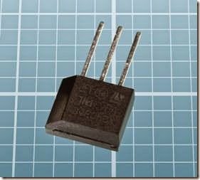
SCR packages reflect their design for a wide range of voltages and currents. Figure 1-3 shows an SCR designed for on-state current of 4A RMS (i.e., measured as the root mean square of the alternating current). Among its applications are small-engine ignition and crowbar overvoltage protection, so named because it shorts a power supply directly to ground, much like a crowbar being dropped across the terminals of a car battery (but hopefully with a less dramatic out- come). See Figure 1-15.

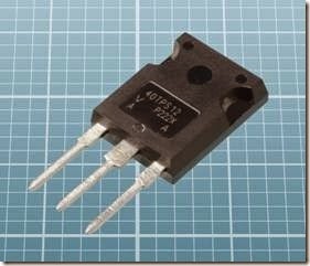
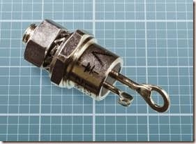
In Figure 1-4, the SCR can handle up to 800V repetitive peak off-state voltage and 55A RMS. Pos- sible applications include AC rectification, crow- bar protection, welding, and battery charging. The component in Figure 1-5 is rated for 25A and 50V repetitive peak off-state voltage. To assess the component sizes, bear in mind that the graph line spacing is 0.1”.

clip_image010

Figure 1-3. SCR rated for 400V repetitive off-state volt- age, no greater than 4A RMS.

clip_image012

Figure 1-4. SCR rated for 800V repetitive off-state volt- age, no greater than 55A RMS.

Internal Configuration

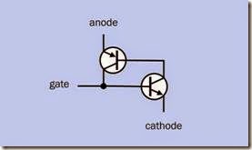
The function of an SCR can be imagined as being similar to that of a PNP transistor paired with an NPN transistor, as shown in Figure 1-6. In this simplified schematic, so long as zero voltage is applied to the “gate” wire, the lower (NPN) tran- sistor remains nonconductive. Consequently, the upper (PNP) transistor cannot sink current, and this transistor also remains nonconductive.

When voltage is applied to the “gate,” the lower transistor starts to sink current from the upper transistor. This switches it on. The two transistors now continue to conduct even if power to the “gate” is disconnected, because they have cre- ated a positive feedback loop.

clip_image015

Figure 1-5. Stud-packaged SCR rated for 50V repetitive off-state voltage, no greater than 25A RMS.

clip_image017

Figure 1-6. An SCR behaves similarly to an NPN and a PNP transistor coupled together.

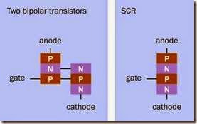
Figure 1-7 shows the same two transistors in simplified form as sandwiches of p-type and n-type silicon layers (on the left), and their combination in an SCR (on the right). Although the actual con- figuration of silicon segments is not as simple or as linear as this diagram suggests, the SCR can be described correctly as a PNPN device.

An SCR is comparable with an electromagnetic latching relay, except that it works much faster and more reliably.

clip_image019

Figure 1-7. The two transistors from the previous figure are shown here in simplified form as two stacks of p-type and n-type silicon layers. These layers are combined in an SCR, on the right.

Breakdown and Breakover Voltage

 The curves in Figure 1-8 illustrate the behavior of a hypothetical SCR, and can be compared with the curves shown for a diac in Figure 2-5 and atriac in Figure 3-10. Beginning with zero voltage applied between anode and cathode, and zero current flowing (i.e., at the center origin of the graph), if we apply a voltage at the anode that is increasingly negative relative to the cathode (i.e., we attempt to force the SCR to allow negative current flow), we see a small amount of leakage, indicated by the darker blue area (which is not drawn to scale). Finally the breakdown voltage is reached, at which point the negative potential overcomes the SCR and its impedance drops rap- idly, allowing a surge of current to flow, probably damaging it.

Alternatively, starting once again from the center, if we apply a voltage at the anode that is increasingly positive relative to the cathode, two consequences are possible. The dashed curve assumes that there is zero voltage at the gate, and shows that some leakage occurs until the applied potential at the anode reaches the break- over voltage, at which point the SCR allows a large current flow, which continues even when the voltage decreases.

clip_image021

Figure 1-8. The solid curve shows current passing be- tween the anode and cathode of a hypothetical SCR for varying voltages, while a triggering voltage is applied to the gate. The dashed curve assumes that no triggering voltage is applied to the gate.

In practice, the SCR is intended to respond to a positive gate voltage. Under these circumstances, its behavior is shown by the solid curve in the top-right quadrant in Figure 1-8. The SCR be- gins to conduct current without having to reach the breakover voltage at the anode.

• When used as it is intended, the SCR should not reach breakdown or breakover voltage levels.

SCR Concept Demo

In Figure 1-9, pushbutton S1 applies voltage to the gate of the SCR, which puts the SCR in self- sustaining conductive mode. When S1 is re- leased, the meter will show that current continues to pass between the anode and the cathode. The X0403DF SCR suggested for this circuit has a holding current of 5mA, which a 5VDC supply should be able to provide with the 1K resistor in the circuit. If necessary, this resistor can be reduced to 680Ω.

Now if pushbutton S2 is pressed, the flow is interrupted. When S2 is released, the flow will not resume. Alternatively, if pushbutton S3 is pressed while the SCR is conducting current, the flow is diverted around the SCR, and when the push- button is released, the flow through the SCR will not resume. Thus, the SCR can be shut down ei- ther by a normally closed pushbutton in series with it (which will interrupt the current), or a nor- mally open pushbutton in parallel with it (which will divert the current).

clip_image023

Figure 1-9. In this test circuit, S1 triggers the SCR, while S2 or S3 will stop it. See text for additional details.

The test circuit is shown installed on a bread- board in Figure 1-10. In this photograph, the red and blue wires supply a minimum of 5VDC. The two red buttons are tactile switches, the one at top left being S1 in the schematic while the one at bottom right is S3. The large switch with a rec- tangular button is S2; this is normally closed, and opens when pressed. The X0403DF SCR is just below it and to the right. The square blue trim- mer is set to the midpoint of its range.

AC Current Applications

If the SCR is used with alternating current, it stops conducting during each negative cycle, and is retriggered in each positive cycle. This suggests one of its primary applications, as a controllable rectifier that can switch rapidly enough to limit

the amount of current that passes through it during each cycle.

clip_image025

Figure 1-10. A breadboarded version of the SCR test circuit. The two red buttons correspond with S1 and S3 in the schematic, while the large rectangular button at top right opens S2. See text for details.

Variants

SCRs are available in surface-mount, through- hole, and stud packages, to handle increasing currents and voltages. Some special-purpose SCRs can control currents of hundreds of amps, while high-power SCRs are used to switch thou- sands of amps at more than 10,000V in power distribution systems. They are too specialized for inclusion in this encyclopedia.

Typical power ratings for SCRs in general use are summarized in the next section.

Values

Any SCR will impose a forward voltage drop, which typically ranges from around 1V to 2V, de- pending on the component.

Because SCRs are often used to modify AC wave- forms, the current that the component can pass is usually expressed as the root mean square (RMS) of its peak value.

Commonly Used Abbreviations

• VDRM Maximum repetitive forward voltage that may be applied to the anode while no voltage is applied to the gate (i.e., when the SCR is not in conductive mode).

• VRRM Maximum repetitive reverse voltage that may be applied to the anode while no voltage is applied to the gate (i.e., when the SCR is not in conductive mode).

• VTM Maximum on-state voltage while the SCR is in conductive mode. T indicates that this value changes with temperature.

• VGM Forward maximum gate voltage.

• VGT Minimum gate voltage required to trig- ger.

• VGD Maximum gate voltage that will not trig- ger.

• IDRM Peak repetitive forward blocking cur- rent (i.e., maximum leakage).

• IRRM Peak repetitive reverse blocking current (i.e., leakage in the off state).

• IGM Maximum forward gate current.

• IT(RMS) Maximum RMS current between anode and cathode while the SCR is in con- ductive mode. T indicates that this value changes with temperature.

• IT(AV) Maximum average current between anode and cathode while the SCR is in con- ductive mode. T indicates that this value changes with temperature.

• IGT Maximum gate current required to trigger.

• IH Typical holding current.

• IL Maximum latching current.

• TC Case temperature, usually expressed as an acceptable range.

• TJ Operating junction temperature, usually expressed as an acceptable range.

Surface-mount variants may tolerate maximum anode-cathode currents that typically range from 1A to 10A. Maximum voltages as high as 500V are allowed in some cases. Leakage in the “off” state may be as high as 0.5mA or as low as 5µA. Gate trigger voltage is likely to range from 0.8V to 1.5V, and trigger current of 0.2mA to 15mA is typical.

Through-hole variants may be packaged in TO-92 format (like discrete transistors) or, more commonly, in TO-220 format (like a typical 1A voltage regulator). They may be rated for a maximum of 5A up to 50A, depending on the component, with maximum voltages ranging from 50V to 500V. Leakage is similar to surface-mount variants. The gate trigger voltage is typically around 1.5V, and trigger current ranges from 25– 50mA.

A stud-type SCR may have a maximum 50A to 500A current rating, although some components are capable of tolerating even higher values. Maximum voltages of 50V to 500V are possible. Leakage is likely to be higher than in other for- mats, with 5mA to 30mA being common. The gate trigger voltage is typically 1.5 to 3V, and trigger current may range from around 50mA to 200mA.

How to Use It

Although other applications are possible, in practice SCRs have two main applications:

• Phase control, which interrupts each positive phase of an AC power supply. It can moderate the speed of a motor or the heat generated by a resistive load.

• Overvoltage protection. This can safeguard sensitive components in a circuit where there is a DC power supply.

SCRs are often incorporated in ground-fault circuit interruptors (although not usually as dis- crete components) and in automotive ignition systems.

Phase Control

Phase control is a convenient way to control or limit the AC power delivered to a load by abbreviating each pulse in the AC waveform. This is done by adjusting the gate voltage so that the SCR blocks the first part of each positive phase, then conducts the remainder, and then stops conducting below its holding level. The SCR will then block the reversed flow in the negative phase of the AC waveform, but an additional SCR with opposite polarity can be added.

This is a form of pulse-width modulation. It is highly efficient, as the effective internal resistance of the SCR is either very high or very low, and the component does not waste significant energy in the form of heat.

On a graph showing the fluctuating voltage of an AC waveform, a single cycle is customarily divided into four stages: (1) zero voltage, (2) maximum positive voltage, (3) zero voltage, (4) minimum negative voltage, all measurements being made between the live side of the supply and the neutral side of the supply.

The cycle then repeats. Its transitions are often referred to as phase angles of 0 degrees, 90 degrees, 180 degrees, and 270 degrees, as shown in Figure 1-11.

The fluctuating voltage in an AC power supply is proportional with the sine of the phase angle. This concept is illustrated in Figure 1-12. If an imaginary point (shown as a purple dot) is moving in a circular path counterclockwise at a constant speed, its vertical distance (shown in green) above or below the X axis (horizontal centerline) can represent an AC voltage corresponding with the angle (shown as purple arcs) of the circle radius to the point, each angle being measured from at the center relative to a start position at right on the X axis.

When an SCR is used for phase control, the point at which it starts to conduct may be anywhere from 0 to almost 180 degrees. This is achieved by diverting a small amount of the AC power into an RC network attached to the gate of the SCR, as shown in Figure 1-13. The capacitor in this schematic introduces a delay that can be varied by the potentiometer. This enables the SCR to be triggered even after the peak of the AC power signal. In Figure 1-14, the AC power is shown by the center (green) curve, and the slightly delayed, reduced voltage at the gate is shown by the upper, purple curve. When the gate voltage rises to the trigger level, it causes the SCR to be- gin conducting current, creating an abbreviated output shown in the bottom curve. In this way, triggering from an AC phase angle of 0 degrees to almost 180 degrees is possible. The phase angle where the SCR begins to allow conduction is known as the conduction angle.

If two SCRs with opposite polarity are placed in parallel with each other, they can be used to pro- vide phase control on both the positive-going and negative-going sections of an AC cycle. This configuration is used in high-powered devices. A triac is used for the same purpose with lower current.

Six SCRs may be used to control three-phase power.

Overvoltage Protection

The tolerance of an SCR for high current makes it suitable for use in a crowbar voltage limiting circuit.

In Figure 1-15, the SCR does not conduct current (other than a small amount of leakage) until the Zener diode senses a voltage above the maxi- mum level considered safe. The diode then al- lows power to reach the gate of the SCR. Its im- pedance drops immediately, and the resulting surge of current trips the fuse. After the cause of the overvoltage condition is corrected, the fuse can be replaced and the circuit may resume functioning.

A capacitor is included so brief spikes in the power supply will be passed to ground without triggering the SCR. A resistor of around 100Ω ensures that the gate voltage of the SCR remains near zero during normal operation. When the Zener diode starts to conduct current, the resistor acts as a voltage divider with the diode, so that sufficient voltage reaches the SCR to activate it.

This circuit may be unsuitable for low-voltage power supplies, because the Zener diode has to be chosen with a high enough rating to prevent small power fluctuations from tripping it. Bearing in mind that the real triggering voltage of the diode may be at least plus-or-minus 5% of its rated voltage, the diode may have to be chosen with at least a 6V rating in a 5V circuit, and it may not be activated until the voltage is actually 6.5V. This may be insufficient to protect the components being used with the power supply.

clip_image027

Figure 1-11. An AC waveform is customarily measured in degrees of phase angle.

What Can Go Wrong

Like other semiconductors, an SCR can be adversely affected by excessive heat. Usual precautions should be taken to allow sufficient ventilation and heat sinking, especially when components are moved from an open prototyping board to an enclosure in which crowding is likely.

Unexpected Triggering Caused by Heat

On a datasheet, the values for triggering current and holding current are valid only within a recommended temperature range. A buildup of heat can provoke unexpected triggering.

Unexpected Triggering Caused by Voltage

A very rapid increase in forward voltage at the anode can induce a triggering voltage in the gate by capacitive coupling. As a result, the SCR can trigger itself without any external application of gate voltage. This is sometimes known as dv/dt triggering. If necessary, a snubber circuit can be added across the anode input to prevent sudden voltage transitions.

clip_image030

Figure 1-12. The fluctuating voltage of an AC power sup- ply (shown as vertical green lines) is proportional with the sines of the angles (purple arcs) in this diagram. The angles are referred to as phase angles.

Confusion of AC and DC Ratings

 The on-state current for an SCR is averaged only over the width of each pulse that the SCR actually conducts. It is not time-averaged over an entire AC cycle, and it will be different again from a DC rating. Care must be taken to match the current rating with the way in which the component will actually be used.

Maximum Current versus Conduction Angle

Current-carrying capability will be very significantly affected by the length of the duty cycle when the SCR is being used to abbreviate each positive AC pulse. When the SCR imposes a 120- degree conduction angle, it may be able to handle twice the average on-state current as when it is imposing a 30-degree conduction angle. The manufacturer’s datasheet should include a graphical illustration of this relationship. If an SCR is chosen for a high conduction angle, and the angle is later reduced, overheating will result, and damage is likely.

clip_image032

Figure 1-13. In this schematic, an SCR is used to apply phase control, adjusting the power that passes through a load.

Confusing Symbols

When reading a schematic, unfortunate errors can result from failure to distinguish between the symbol for a programmable unijunction transistor (PUT) and the symbol for an SCR. The characteristics of a PUT are described in Volume 1 of this encyclopedia.

clip_image034

Figure 1-14. If the AC power applied to the anode of an SCR (center) is reduced in voltage and delayed slightly by an RC network, it can trigger the SCR (top), causing it to pass only an abbreviated segment of each positive AC pulse (bottom).

clip_image036

Figure 1-15. In this schematic, an SCR is used to provide crowbar overvoltage protection for sensitive components.


diac:What It Does,Symbol Variants,How It Works,Switching AC,Variants,Values,What Can Go Wrong,Unexpected Triggering Caused by Heat,Low-Temperature Effects and Manufacturing Tolerances.

diac

A diac is a self-triggering type of thyristor. Its name is said to be derived from the phrase “diode for AC,” and because it is not an acronym, it is not usually capitalized.

A thyristor is defined here as a semiconductor having four or more layers of p-type and n-type silicon. Because the thyristor predated integrated circuits, and in its basic form consists of a single multilayer semiconductor, it is categorized as a discrete component in this encyclopedia. When a thyristor is combined with other components in one pack- age (as in a solid-state relay) it is considered to be an integrated circuit.

Other types of thyristor are the SCR (silicon-controlled rectifier) and the triac, each of which has its own entry in this encyclopedia.

Thyristor variants that are not so widely used, such as the gate turn-off thyristor (GTO) and

silicon-controlled switch (SCS), do not have entries here.

What It Does

The diac is a bidirectional thyristor with only two terminals. It blocks current until it is subjected to sufficient voltage, at which point its impedance drops very rapidly. It is primarily used to trigger a triac for purposes of moderating AC power to an incandescent lamp, a resistive heating element, or an AC motor. The two leads on a diac have identical function and are interchangeable.

By comparison, a triac and an SCR are thyristors with three leads, one of them being referred to as the gate, which determines whether the com- ponent becomes conductive. A triac and a diac allow current to flow in either direction, while an SCR always blocks current in one direction.

Symbol Variants

The schematic symbol for a diac, shown in Figure 2-1, resembles two diodes joined togeth- er, one of them inverted relative to the other. Functionally, the diac is comparable with a pair of Zener diodes, as it is intended to be driven be- yond the point where it becomes saturated. Be- cause its two leads are functionally identical, they do not require names to differentiate them. They are sometimes referred to as A1 and A2, in rec- ognition that either of them may function as an anode; or they may be identified as MT1 and MT2, MT being an acronym for “main terminal.”

clip_image005

Figure 2-1. Symbol variants to represent a diac. All four are functionally identical.

The symbol may be reflected left to right, and the black triangles may have open centers. All of these variants mean the same thing. Occasion- ally the symbol has a circle around it, but this style is now rare.

When only a moderate voltage is applied (usually less than 30V) the diac remains in a passive state and will block current in either direction, al- though a very small amount of leakage typically occurs. When the voltage exceeds a threshold known as its breakover level, current can flow, and the diac will continue to conduct until the current falls below its holding level.

A sample diac is shown in Figure 2-2.

clip_image007

Figure 2-2. Because a diac is not intended to pass significant current, it is typically packaged in a small format. The graph squares in the photograph each measure 0.1”.

How It Works

Figure 2-3 shows a circuit that demonstrates the conductive behavior of a diac.

clip_image010

Figure 2-3. A test circuit to demonstrate the behavior of a diac. See text for details.

When the pushbutton is held down, current from the positive side of the AC supply flows through the diode and the 470K resistor to the capacitor. The diac is not yet conductive, so the capacitor accumulates a potential that can be monitored with the volt meter. After about 30 seconds, the charge on the capacitor reaches 32V. This is the breakover voltage for this particular diac, so it becomes conductive. The positive side of the capacitor can now discharge through the diac and the 1K series resistor to ground.

If the pushbutton is released at this moment, the meter will show that the capacitor discharges to a potential below the holding level of the diac. The capacitor now stops discharging because the diac has ceased being conductive.

If the pushbutton is held down constantly, the meter will show the capacitor charging and then discharging through the diac repeatedly, so that the circuit behaves as a relaxation oscillator. The 1K series resistor is included to protect the diac from excessive current. If a standard quarter-watt resistor is used, it should not become unduly warm because current passes through it only intermittently.


• Because this circuit uses 115VAC, basic pre- cautions should be taken. The fuse should not be omitted, the capacitor should be rat- ed for at least 50V, and the circuit should not be touched while it is connected to the pow- er source. Breadboarding a circuit using this voltage requires caution and experience, as wires can easily come loose, and compo- nents can be touched accidentally while they are live.

Figure 2-4 shows the test circuit on a breadboard. The red and blue leads at the top of the photo- graph are from a fused 115VAC power supply. The live side of the supply passes through a diode to a pushbutton switch that has a rectangular black cap. A 470K resistor connects the other side of the switch to the positive side of a 100µF elec- trolytic capacitor, and also to the diac (small blue component). A 1K resistor connects the other end of the diac back to the negative side of the capacitor, which is grounded. The yellow and blue wires leaving the photograph at the left are connected with a volt meter, which is not shown.

clip_image014

Figure 2-4. A breadboarded version of the diac test cir- cuit. See text for details.

The behavior of a diac is also illustrated in Figure 2-5, which can be compared with the curves in Figures 3-10 and 1-8, depicting the behavior of a triac and an SCR respectively.

clip_image012

Figure 2-5. The curve shows current passing through a diac when various voltages are applied.

Switching AC

The diac cannot function as a switch, because it lacks the third terminal which is found in a triac, an SCR, or a bipolar transistor. However, it is well suited to drive the gate of a triac, because the behavior of a diac is symmetrical in response to opposite voltages, while the triac is not. If an AC voltage applied to a diac is adjusted with a po- tentiometer in an RC circuit, the diac will pass along a portion of each positive or negative pulse, and will delay it by a brief amount of time determined by the value of the capacitor in the RC circuit and the setting of the potentiometer. This is known as phase control, as it controls the phase angle at which the diac allows current to flow.

See Figure 3-13 for a schematic showing a diac driving a triac. See Figures 1-14 and 3-11 for graphs illustrating phase control. See “Phase Control” for a discussion of phase in AC wave- forms.

Variants

Diacs are available in through-hole and surface- mount formats. Because they are not intended to handle significant current, no heat sink is included.

A sidac behaves very similarly to a diac, its name being derived from “silicon diode for alternating current.” Its primary difference from generic di- acs is that it is designed to reach its breakover voltage at a higher value, typically 120VAC or 240VAC.

Values

When performing its function to trigger a triac, a diac is unlikely to pass more than 100mA.

The breakover voltage of a diac is usually be- tween 30V and 40V, with a few versions designed for up to 70V. When the diac starts to conduct, its on-state impedance is sufficient to reduce the voltage significantly, with 5V being a typical min- imum output voltage.

Although the rise time when a diac responds is very brief (around 1µs), the component is not ex- pected to run at a high frequency. It will normally be used with 50Hz or 60Hz AC to trigger a triac. For this reason, its repetitive peak on-state cur- rent is usually specified at no more than 120Hz.

Abbreviations in datasheets are likely to include:

• VBO Breakover voltage (sometimes may be specified as latching voltage, which for a diac is the same thing).

• VBO1 – VBO2 Breakover voltage symmetry. The hyphen is intended as a minus sign, so that this value is the maximum difference be- tween breakover voltage in each direction.

• VO Minimum output voltage.

• ITRM Repetitive peak on-state current.

• IBO Breakover current, usually the maximum required, and less than 20µA.

• IR Maximum leakage current, usually less than 20µA.

• TJ Operating junction temperature, usually expressed as an acceptable range.

What Can Go Wrong

Like other semiconductors, a diac is heat sensi- tive. Usual precautions should be taken to allow sufficient ventilation and heat sinking, especially when components are moved from an open pro- totyping board to an enclosure in which crowd- ing is likely.

Unexpected Triggering Caused by Heat

On a datasheet, a value for breakover current is valid only within a recommended temperature range. A buildup of heat can provoke unexpec- ted triggering.

Low-Temperature Effects

A higher breakover voltage will be required by a diac operating at low temperatures, although the variation is unlikely to be greater than plus- or-minus 2% within a normal operating range. Temperature has a much more significant effect on a triac.

Manufacturing Tolerances

The breakover voltage for a diac is not adjustable, and may vary significantly between samples of the component that are supposed to be identical. The diac is not intended to be used as a precision component. In addition, while its break- over voltage should be the same in either direction, a difference of plus-or-minus 2% is possible (1% in some components).


Huffman Trees.

Huffman Trees

Some useful definitions:

Code word: Encoding a text that comprises n characters from some alphabet by assigning to each of the text’s characters some sequence of bits. This bits sequence is called code word

Fixed length encoding: Assigns to each character a bit string of the same length.

Variable length encoding: Assigns code words of different lengths to different characters.

Problem:

How can we tell how many bits of an encoded text represent ith character?

We can use prefix free codes

Prefix free code: In Prefix free code, no codeword is a prefix of a codeword of another character.

• Binary prefix code :

o The characters are associated with the leaves of a binary tree.

o All left edges are labeled 0

o All right edges are labeled 1

o Codeword of a character is obtained by recording the labels on the simple path from the root to the character’s leaf.

o Since, there is no simple path to a leaf that continues to another leaf, no codeword can be a prefix of another codeword

Huffman algorithm:

• Constructs binary prefix code tree

• By David A Huffman in 1951.

• Huffman’s algorithm achieves data compression by finding the best variable length binary encoding scheme for the symbols that occur in the file to be compressed. Huffman coding uses frequencies of the symbols in the string to build a variable rate prefix code

o Each symbol is mapped to a binary string

o More frequent symbols have shorter codes

o No code is a prefix of another code

• Huffman Codes for Data Compression achieves 20-90% Compression

Construction:

Step 1: Initialize n one-node trees and label them with the characters of the alphabet.

Record the frequency of each character in its tree’s root to indicate the tree’s weight. (More generally the weight of a tree will be equal to the sum of the frequencies in the tree’s leaves)

Step 2: Repeat the following operation until a single tree is obtained.

“Find two trees with smallest weight. Make them the left and right sub-tree of a new tree and record the sum of their weights in the root of the new tree as its weight”

Example:

Construct a Huffman code for the following data:

image

image


Dijkstra’s Algorithm – to find Single Source Shortest Paths.

Dijkstra’s Algorithm

– to find Single Source Shortest Paths

Some useful definitions:

Shortest Path Problem: Given a connected directed graph G with non-negative weights on the edges and a root vertex r, find for each vertex x, a directed path P (x) from r to x so that the sum of the weights on the edges in the path P (x) is as small as possible.

Algorithm

• By Dutch computer scientist Edsger Dijkstra in 1959.

• Solves the single-source shortest path problem for a graph with nonnegative edge weights.

• This algorithm is often used in routing.

E.g : Dijkstra’s algorithm is usually the working principle behind link-state routing protocols

ALGORITHM Dijkstra(G, s)

//Input: Weighted connected graph G and source vertex s

//Output: The length Dv of a shortest path from s to v and its penultimate vertex Pv for every vertex v in V

//initialize vertex priority in the priority queue Initialize (Q)

for every vertex v in V do

image

image

The method

Dijkstra’s algorithm solves the single source shortest path problem in 2 stages.

Stage 1: A greedy algorithm computes the shortest distance from source to all other nodes in the graph and saves in a data structure.

Stage 2 : Uses the data structure for finding a shortest path from source to any vertex v.

  • At each step, and for each vertex x, keep track of a “distance” D(x) and a directed path P(x) from root to vertex x of length D(x).

  •  Scan first from the root and take initial paths P( r, x ) = ( r, x ) with D(x) = w( rx ) when rx is an edge, D(x) = when rx is not an edge.

For each temporary vertex y distinct from x, set

D(y) = min{ D(y), D(x) + w(xy) }

Example:

Apply Dijkstra’s algorithm to find Single source shortest paths with vertex a as the source.

image

Solution:

Length Dv of shortest path from source (s) to other vertices v and Penultimate vertex Pv for every vertex v in V:

image

Conclusion:

• Doesn’t work with negative weights

• Applicable to both undirected and directed graphs

• Use unordered array to store the priority queue: Efficiency = Θ(n2)

• Use min-heap to store the priority queue: Efficiency = O(m log n)