encoder:What It Does,Schematic Symbol,Similar Devices,How It Works,Variants,Values,How to Use It,Cascaded Encoders and What Can Go Wrong.

encoder

In this encyclopedia, an encoder is a digital chip that converts a decimal-valued input into a binary-coded output.

The term “encoder” may alternatively refer to a rotational encoder (also known as a rotary encoder) which has a separate entry in Volume 1 of this encyclopedia. The term may also describe a code hopping encoder, which is an encryption device used in keyless entry systems for automobiles.

What It Does

An encoder is a logic chip that receives an input consisting of an active logical state on one of at least four input pins, which have decimal values from 0 upward in increments of 1. The encoder converts the active pin number into a binary value represented by logic states on at least two output pins. This behavior is opposite to that of a decoder.

Encoders are identified in terms of their inputs and outputs. For example:

• 4-to-2 encoder (four input pins, two output pins)

• 8-to-3 encoder (eight input pins, three out- put pins)

• 16-to-4 encoder (sixteen input pins, four out- put pins)

In the early days of computing, encoders processed interrupts. This application is now rare, and relatively few encoder chips are still being manufactured. However, they are still useful in small devices—for example, if a large number of inputs must be handled by a microcontroller that has insufficient pins to receive data from each individually.

Schematic Symbol

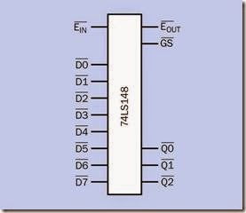
Like other logic-based components, the encoder does not have a specific schematic symbol and can be represented by a plain rectangle as in Figure 14-1, with inputs on the left and outputs on the right. The bars printed above some of the abbreviations indicate that an input or output is active-low. In this chip, the 74LS148, all inputs and outputs are active-low.

Generally speaking, inputs labeled D0, D1, D2… are used for data input, although they may simply be numbered, with no identifying letter. The encoded outputs are typically identified as Q0, Q1, Q2… or A0, A1, A2… with Q0 or A0 designating the least significant bit in the binary number.

Pins labeled E and GS are explained in the following section.

clip_image005

Figure 14-1. While no specific schematic symbol exists for an encoder chip, this style is commonly used. Shown here is a 16–to–4 encoder with active-low inputs and outputs.

Similar Devices

The similarities and differences between encoder, decoder, multiplexer, and demultiplexer can cause confusion.

• In an encoder, an active logic state is applied to one of four or more input pins, while the rest remain in an inactive logic state. The in- put pin number is converted to a binary code which is expressed as a pattern of logic states on two or more output pins.

• In a decoder, a binary number is applied as a pattern of logic states on two or more input pins. This value determines which one of four or more output pins will have an active logic state, while the rest remain in an inactive logic state.

• A multiplexer can connect a choice of multiple inputs to a single output, for data transfer. The logic state of an enable pin, or a bi- nary number applied as a pattern of logic states to multiple control pins, chooses which input should be connected with the output pin. The alternative term data selector evokes the function of this device more clearly.

• An analog multiplexer may allow its inputs and outputs to be swapped, in which case it becomes a demultiplexer. It can connect a single input to one of multiple outputs, for data transfer. The logic state of an enable pin, or a binary number applied as a pattern of logic states to multiple control pins, chooses which output should be used. The alternative term data distributor evokes the function of this device more clearly.

How It Works

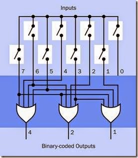
An encoder contains logic gates. The internal logic of an 8-to-3 encoder is shown in Figure 14-2, where the darker blue rectangle rep- resents the chip. The switches in this figure are external and are included only to clarify the concept. An open switch is imagined to provide an inactive logic input, while a single closed switch provides an active logic input. (Multiple active inputs can be handled by a priority encoder, de- scribed below).

Each input switch has a numeric status from 1 to

7. The switch with value 0 does not make an internal connection, because the output from the OR gates is 000 by default.

The logic state of each OR output represents a binary number, weighted with decimal values 1, 2, and 4, as shown at the bottom of the figure. Thus, if switch 5 is pressed, by tracing the connections it is clear that the outputs of OR gates 4 and 1 become active, while the output from gate 2 remains inactive. The values of the active out- puts thus sum to 5 decimal.

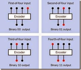
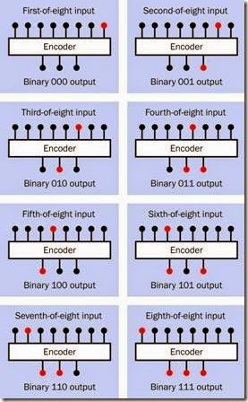
Figure 14-3 shows the outputs for all possible in- put states of a 4-to-2 encoder. Figure 14-4 shows the outputs for all possible input states of an 8- to-3 encoder. These diagrams assume that a high logic state is an active logic state, on input or output. This is usually the case.

clip_image008

Figure 14-2. A simplified simulation of the internal logic of an 8-to-3 encoder. The dark blue rectangle indicates the space inside the chip. The external switches are in- cluded only to clarify the concept. An encoder chip would have an Enable line to create an active output.

clip_image010

Figure 14-3. The four possible inputs of a 4-to-2 encoder (top of each panel) and the encoded outputs (below).

clip_image012

Figure 14-4. The eight possible inputs of an 8-to-3 en- coder (at the top of each panel), and the encoded outputs (below). Note that one input of an encoder must always be logic-high. All logic-low inputs are not a valid state.

Unlike ripple counters, where propagation de- lays can reduce the overall response time of the component, decoders respond within two or three nanoseconds.

Variants

A simple encoder assumes that only one input pin can be logically active at a time. A priority encoder assigns priority to the highest-value input pin if more than one happens to receive an active input. It ignores any lower-value inputs. An ex- ample is the 74LS148, which is an 8-to-3 chip.

A few encoders feature three-state outputs (also known as tri-state), in which a high-impedance or “floating” output state is available in addition to the usual high and low logic states. The high- impedance state allows multiple chips to share an output bus, as those that are in high- impedance mode appear to be disconnected. This is useful if two or more encoders are cascaded to handle a larger number of inputs.

Values

As is the case with other logic chips, most en- coders in the through-hole 74xx series are in- tended for 5VDC power supply while the older 4000 series may tolerate up to 18VDC. Surface- mount versions may use voltages as low as 2VDC.

See the section on logic gates in Chapter 10 for a discussion of acceptable high and low input states. On the output side, the 4000 series chips are able to source less than 1mA at 5VDC, but the 74HCxx series can manage around 20mA.

How to Use It

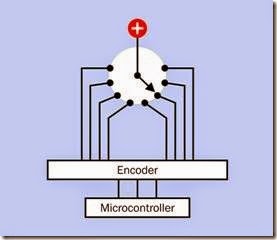
Suppose that a microcontroller should respond to an eight-position rotary switch. Because the switch cannot be turned to more than one position at a time, all of its eight contacts can be connected with the inputs on an encoder, which will deliver a 3-bit binary number to three inputs of the microcontroller. Code inside the microcontroller then interprets the pin states.

This is shown in Figure 14-5. Pulldown resistors would be needed on the input pins of the en- coder, to prevent them from floating when they are not connected by the rotary switch. They have been omitted from this diagram for simplicity. Debouncing the switch would be handled by the microcontroller.

Other forms of input may be used instead of a rotary switch. For example, the outputs from eight comparators or eight phototransistors could be passed through an encoder.

clip_image016

Figure 14-5. Output from an eight-input rotary switch could be connected through an 8-to-3 encoder to provide input to a microcontroller using a reduced number of pins. Pulldown resistors have been omitted for simplicity.

Cascaded Encoders

Encoders are often provided with features to facilitate handling additional inputs via multiple chips. Typically, a second Enable pin is provided, as an output that connects with the Enable input of the preceding chip. This preserves the priority function, so that an input on the second chip prevents any additional input to the first chip from affecting the output. In a datasheet, the en- able pins may be labeled EIN and EOUT, or EI and EO.

In addition, a GS pin will be included, meaning “Group Select.” It is logically active only when the encoder is enabled and at least one input is active. The GS pin of the most-significant encoder provides an additional binary digit.

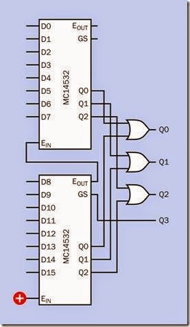
The outputs from two encoders can be linked via OR gates, as shown in Figure 14-6, where the lower chip’s GS output provides the most significant bit of a four-bit binary number.

clip_image018

Figure 14-6. Two eight-bit encoders can be cascaded to handle 16 separate inputs. In this example, the encoders use active-high logic.

What Can Go Wrong

Problems that are common to all digital chips are summarized in the section on logic gates in “What Can Go Wrong” on page 105.

See “What Can Go Wrong” on page 149 in the entry describing decoders for a list of more specific problems that also afflict encoders.


counter:What It Does,Schematic Representation,How It Works,Modulus and Modulo,Clock Sources,Rising Edge and Falling Edge,Multiple Stages,Single and Dual,What Can Go Wrong,Lock-Out,Asynchronous Artifacts and Noise.

counter

The term counter is used here to mean a digital-logic chip. A counter could be built from discrete transistors, but this approach is obsolete. Counters may also be devised from parts such as multiple relays, or a solenoid advancing a ratchet wheel, but such electro- mechanical devices are not included in this encyclopedia.

In this encyclopedia, a counter by definition has binary-weighted outputs with values 1, 2, 4, 8…. in decimal notation. The exception to this rule is a ring counter, which does not have binary-weighted outputs but is included here because its name identifies it as a counter. A shift register may be used as a ring counter, but is more versatile and has many other functions; hence it has a separate entry.

Gray code counters, in which successive outputs differ by only one binary digit, are not described in this encyclopedia.

What It Does

A counter can be used to count events, or can measure time in convenient intervals if it is connected with a component such as a quartz crystal that operates at a precise and reliable frequency. The counter receives input pulses (usually referred to as a clock input) and counts a pre- determined number of them before restarting from the beginning. It will repeat in this fashion so long as power is connected, and the clock pulses continue, and a reset signal is not supplied.

Almost all counters create some form of output during the count. Most commonly, the output is a pattern of high and low states expressing the number of clock pulses in binary code. Where a counter counts to a very high number before re- cycling, some intermediate binary digits may be omitted.

While standalone counter chips are not as widely used now as in the early days of computing, they still find application in industrial processes, small devices, and education, and can be used to control incremental devices such as stepper motors. They can be used in conjunction with microcontrollers.

Schematic Representation

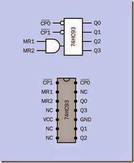
No specific logic symbol exists for a counter. It is most often shown in a schematic as a rectangle with clock input(s) and clear input(s) on the left and outputs on the right. An example appears in Figure 13-1, above a representation of the physical chip and its pinouts. The meaning of the abbreviations identifying the inputs, outputs, and control functions will be found in “How It Works” on page 132. Because the two MR inputs for this particular counter are ANDed inside the chip,

the AND symbol is included with the counter symbol.

clip_image005

Figure 13-1. Typical schematic representation of a counter, compared with the pinouts of the actual component.

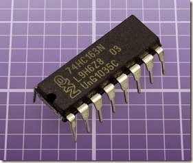
A counter chip is shown in Figure 13-2.

clip_image007

Figure 13-2. The 74HC163 shown in this photograph is a 4-bit synchronous counter capable of being preloaded with a starting value, and able to do a synchronous reset.

How It Works

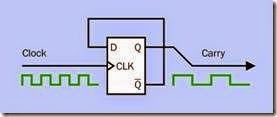
A counter is built from a chain of flip-flops, with each one triggering the next. JK, T-type, or D- type flip-flops may be used. For a thorough description of a flip-flop, see Chapter 11. In Figure 13-3, a D-type flip-flop is shown, triggered by each rising clock pulse.

clip_image010

Figure 13-3. When the complementary (NOT-Q) output from a D-type flip-flop is connected back to its input, the Q output frequency is half of the clock input frequency. See text for additional details.

Initially the Q output of the flip-flop is low, so its NOT-Q output (identified by Q with a bar above it) is high. This feeds back to the D input, but has no effect until the rising edge of the next clock pulse copies the high D input to the Q output. The Q output is now latched high while the NOT- Q output is latched low and feeds back to the D input. The triggering event has passed, so the low D input does not have any immediate effect. The rising edge of the next clock pulse copies the low state of the D input to the output, and changes the NOT-Q output to high, causing the cycle to repeat. As a result, the output frequency of the flip-flop is one-half of the input frequency from the clock. If the output is carried to the next flip-flop to become its clock input, once again the frequency will be divided by two.

Modulus and Modulo

The modulus of a counter is the number it will count up to, before it repeats. This is sometimes written incorrectly as modulo.

In fact, modulo is the name of an arithmetical operation, often abbreviated as MOD (usually capitalized, even though it is not an acronym). This operation consists of a division sum in which the remainder from the division is the result of the operation. Thus 100 modulo 5 gives a result of 0, because there is no remainder when 100 is divided by 5. But 100 modulo 7 gives a result of 2, because 2 is the remainder of the division operation.

To exacerbate the confusion, MOD is also used as an adjective referring to the modulus of a counter. Thus a MOD-4 counter has a modulus of 4, and a MOD-16 counter has a modulus of 16. As a general rule, when a counter is being described, modulo and MOD will mean the same thing as modulus. This may be confusing to people such as computer programmers who are already familiar with the correct usage of MOD as an arithmetical operator.

In a counter, to obtain a modulus that is not a power of two, logic gates inside the chip can intercept a particular value (such as 1010 binary, which is 10 decimal) and use this as a signal to restart the count at zero. External connections to the chip can achieve the same purpose.

Pin Identifiers

Abbreviations and acronyms are used in data- sheets to identify pin functions. These identifiers have not been standardized, and many variants exist.

CLK is the abbreviation most commonly used for the clock input, sometimes alternatively shown as CK or CP. If it is active-low, or if its falling edge will be active, a bar will be printed above it. Where a printed font does not permit an underscore to be placed in this way, CLK’ (the abbreviation followed by an apostrophe) may be used instead. Often two or more stages of a counter can be separately clocked, and the input pins will be identified with abbreviations such as CLK1 and CLK2, or 1CLK and 2CLK, or CKA and CKB, or CP1 and CP2, or similar.

Where a clock input is edge-triggered, this is indicated by a small triangle. The triangle can be seen in Figure 13-3.

CLR designates a pin which will clear the count and reset it back to zero. This signal is often active-low, indicated by a bar printed above the abbreviation.

In a schematic, a small circle, properly known as a bubble, may be placed at any input which is active-low. On a clock input, the circle indicates that it is falling-edge triggered. See Figure 11-16 for various implementations of symbols with flip- flop schematics.

The CLR operation may be synchronous (the pin state will not be recognized until the next clock pulse) or asynchronous (in which case the pin state overrides the clock and resets the counter immediately). MR stands for “Master Reset,” and has the same function as CLR.

Where two or more counters (or multiple stages within one counter) can be reset separately, more than one clear input will be shown, and may be identified with abbreviations such as CLR1 and CLR2, or MR1 and MR2.

Output pins will almost always be identified as Q0, Q1, Q2 … or QA, QB, QC … up to the maxi- mum necessary to express the modulus. If two or more counters are included in one chip, outputs may be prefixed with an appropriate number. Thus 2Q3 would be the third output in the second counter. Multiple counters in one chip are identified with numbers starting from 1.

Where internal flip-flops are shown, they will have identifiers such as FF1 or FF2. Each flip-flop will have its own clear function, identified as C or CD (the latter meaning “clear data”), and may have inputs labeled D1, D2, D3… in a D-type flip- flop or J and K in a JK flip-flop. See Chapter 11 for an explanation of flip-flop inputs and outputs.

The input to a counter is always imagined to be- gin from the left, and consequently the leftmost flip-flop shown in an internal schematic will ex- press the least significant bit of the current value of the count, even though a binary number is written with the least significant bit in the right- most place.

If a counter is capable of receiving parallel data as an input (explained below) it will have a pin labeled PE for parallel enable. It may also have a CE or CET pin, for count enable.

As is generally the case in logic chips, VCC or V+ are typically used to identify the positive power supply pin, while GND or V- will identify the negative-ground pin. NC means that a pin has no internal connection at all, and consequently re- quires no external connection.

Variants

change in a rapid but incremental sequence from the input to the output. This is also known as an asynchronous counter. Because the final state will not be valid until the clock pulse has rippled all the way through the counter (and through additional counters if they are cascaded together), a ripple counter will tend to suffer from a propagation delay of up to a microsecond. Ripple counters may also create output spikes or momentary transient count values that are invalid. Therefore, they are more suitable for applications such as driving a numeric display than for interfacing at high speed with other logic chips.

All counter chips use binary code internally, and the number of bits (binary digits) in the counter’s modulus will be the same as the number of internal flip-flops. A 4-bit counter (the usual mini- mum) will have a modulus of 24 which is 16. A 21- bit counter (the maximum typically available) will have a modulus of 221 which is 2,097,152. For higher moduli, counters can be chained together, each sending a carry signal to the next. This is known as a cascade.

Multiple counters, with different moduli, may be chained in a single chip. For example, in a digital clock that displays hours and minutes using the 60Hz frequency of an American domestic power supply as its timebase, the initial counting stage will have a modulus of 60, to count individual seconds. The next counting stages will have moduli of 60, 10, and 6, so that they can count from 00 to 59 minutes. Additional stages in the chip will tally hours.

A counter with a parallel input can be preloaded with an initial value (in binary code) from which it may count up or down. A parallel-enable pin may put the counter into a mode where the number can be jam loaded, meaning that it is jammed into the counter regardless of the clock state. Other types of counter are loaded synchronously.

Ripple versus Synchronous

In a ripple counter each internal flip-flop triggers the clock input of the next, so that their states In a synchronous counter, all the flip-flops are clocked simultaneously. A synchronous counter is better suited to operation at high speed.

Of the counter chips available today, about half are synchronous and half are asynchronous.

Ring, Binary, and BCD

A counter that activates output pins one at a time sequentially is said to have a decoded output. It is often referred to as a ring counter. It has the same number of output pins as its modulus. An example is the 4017B chip.

A binary counter is more common and has an encoded output, meaning that it will express the running total of the count in binary code through weighted outputs that typically have (decimal) values of 1, 2, 4, 8, and so on. A modulus-8 counter (often referred to as an octal counter) will require three outputs which represent the binary numbers 000, 001, 010, 011, 100, 101, 110, and 111

(decimal 0 through 7) before going back to 000 and repeating.

A modulus-16 counter, also known as a hexadecimal counter or a divide-by-16 counter, will have a binary output represented by four output pins, counting from 0000 through 1111 (decimal 0 through 15). Four-digit binary counters are very common, and their outputs are compatible with other components such as a decoder, which converts a binary-number input into a ring- counter-style output.

A decade counter is a modulus-10 binary counter. It is described as having a binary-coded decimal output (often expressed with the acronym BCD), using four weighted output pins which represent the numbers 0000, 0001, 0010, 0011, 0100, 0101, 0110, 0111, 1000, and 1001 (decimal 0 through

9) before repeating. Because this counter skips binary outputs from 1010 through 1111 (decimal 10 through 15), it is said to have a shortened modulus.

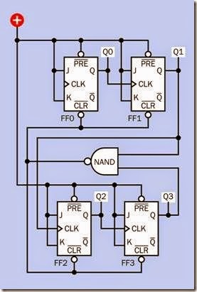
Figure 13-4 shows a schematic diagram of JK flip- flops in a decade ripple counter. The J and K in- puts are all tied to the positive power supply, as this causes the clock input to toggle the output high and low. Note that because the primary in- put is always shown at the left end of the component, the least significant output bit (Q0) is in the leftmost position.

To intercept binary 1010 (decimal 10), an internal NAND gate is used. Its output goes low when its two inputs, from Q1 and Q3, go high. The output from the NAND immediately activates the CLR function on all the flip-flops, so that as soon as the decade counter reaches 1010 (decimal 10), it resets itself to 0.

In this particular chip, the preload for each flip- flop is tied to the positive power supply, so that it is always inactive. In some counters, the pre- load feature of each flip-flop is accessible via pins outside the chip. This creates the potential hazard of preloading the counter with one of the numbers that it normally skips (for instance, 11 decimal in a decade counter). This is referred to as an invalid number or disallowed state. (This use of the term “state” refers only to the binary number stored in the counter’s flip-flops. It has noth- ing to do with the high-state or low-state voltages used to represent binary 0 or 1.)

The counter’s datasheet should include a state diagram showing how the counter will deal with this situation. It may reset itself to a valid value after a maximum of two steps, but this can still cause confusion, depending on the application.

The state diagram for a 74HC192 counter is shown in Figure 13-5.

clip_image012

Figure 13-4. The internal logic of a synchronous decade counter that uses JK flip-flops.

Clock Sources

The clock input may be provided by a timer chip or by an RC network, which has the advantage of being able to run at a relatively low speed for purposes where this is desirable. It may alternatively be provided by a quartz crystal oscillating at a much higher frequency such as 1MHz. Successive counters may be necessary to reduce this value, depending on the application.

In some counters, the clock is built into the chip. More commonly, a resistor and capacitor may be used externally to establish a clock rate in con- junction with logic gates inside the chip. The datasheet for this type of component will include a formula for calculating the clock frequency from the resistor and capacitor values. The 4060B chip is an example.

clip_image014

Figure 13-5. A state diagram shows the transitions that a counter will make from each number to the next (in decimal notation), including the transitions which enable it to exit from disallowed states. This example is for a 74HC192 chip.

Rising Edge and Falling Edge

A counter may be designed to be triggered either by the rising edge or the falling edge of the clock input, or by its high or low logic state. Generally speaking, ripple counters use the falling edge, so that the final output from one counter can be- come the clock input of the next. In other words, when the most significant digit of the first counter changes from a high to low logic state, this transition toggles the least significant bit of the second counter.

Synchronous counters generally use the rising edge of the clock input. If multiple synchronous counters are cascaded, they must all share the same clock signal, and will all change their flip- flop states simultaneously.

Multiple Stages

It is common for a counter chip to contain two or more stages with differing moduli. To take a common example, a divide-by-2 stage and a divide-by-5 stage that are both present in a single chip can be used to create a decade counter by connecting external pins. The extra stages provide a choice of moduli if they are used individually.

Single and Dual

Counter chips may contain two counters of the same modulus. This is known as a dual counter. Dual 4-bit counter chips are common. Each counter can be used separately, or they can be cascaded, in which case the total modulus will be found by multiplying the individual moduli together.

High-State, Low-State, and Three-State Almost all counters use positive logic where a 1 is represented by a high state and 0 by a low state. Some counters allow an additional output state which has a high impedance and is equivalent to an open circuit. This feature is useful when two or more chips share the same output bus. It is discussed in the entry for shift registers in “Three-State Output” on page 126.
Descending Output

Most components only create an ascending count. The output can be converted to a de- scending count by passing each binary state through an inverter, but this will only work properly if the modulus is equal to the number of states. In a BCD counter, its inverted outputs will count from decimal 15 to decimal 6, not from decimal 9 to decimal 0.

A few counters are available which are designed to create a correct descending count. Other counters are available which allow the user to set the mode to ascending or descending. Examples are the 74×190 or 74×192 (where an acronym for the chip family will be substituted for the letter x).

A descending output is useful in combination with a parallel input, where a user may set an initial value from which the counter will descend to 0. With suitable logic, this can enable a user- specified delay period.

Programmable Counters

A programmable counter can usually allow a modulus ranging from 2 to more than 10,000. The counter counts down by dividing an initial number repeatedly with a value that is preset with binary inputs. An example is the 4059B chip.

Examples

Many counter specifications date back to the 4000 family of logic chips. Versions of them sub- sequently became available in the 74xx series, often with the old 4000 part number preceded by 74x (where x is replaced by a designation of the logic family). For example, a version of the 4518B dual BCD chip can be obtained as the 74HC4518. As is the case with all logic chips, this part number will be preceded by letter(s) desig- nating the particular manufacturer, with a suffix added to differentiate minor variants of the chip. The 74xx series has the advantage of higher speed and a greater ability to source or sink cur- rent at its output pins.

Most of the original CMOS chips, such as the 4518B, are still available, even in surface-mount versions. These offer the possible advantage of being able to use a higher power supply voltage.

Many counters offer multiple options such as different modulus values that can be selected by external pin connections. Some chips are tolerant of slow clock frequencies; others are not. Most are edge-triggered, but a few are level triggered. Some, such as the 4518B mentioned above, allow a choice of a rising-edge clock input and falling-edge clock input on different pins. For a specific application, it is really necessary to read a variety of datasheets to select the chip that is most suitable.

Values

As is the case with other logic chips, most counters in the through-hole 74xx series are intended

for 5VDC power supply while the older 4000 series may tolerate up to 18VDC. Surface-mount 74xx versions may use voltages as low as 2VDC.

See the section on logic gates in Chapter 10 for a discussion of acceptable high and low logic- input states. On the output side, the 4000 series chips are able to source or sink less than 1mA at 5VDC, but the 74HCxx series can usually manage around 20mA.

A few counters are capable of delivering more power through additional output stages that can drive LEDs. The 4026B decade counter is still being manufactured, capable of powering modest 7-segment displays. The 4033B has the addition- al option of blanking any leading zeros in a multi- digit display. Other chips that were designed for direct connection to LED numerals have become obsolete as the need for this application has di- minished. The 74C925, 74C926, 74C927, and 74C928 are examples. They may still be found from surplus outlets, but should not be specified in new circuit designs.

What Can Go Wrong

The entry that deals with problems affecting shift registers (see “What Can Go Wrong” on page 128), describes issues which also affect counters. The entry that deals with logic chips (see “What Can Go Wrong” on page 105), describes problems affecting all types of logic chips. In addition, the potential problems listed below are specific to counters.

Lock-Out

This is the condition which occurs if a counter with a shortened modulus is loaded with a binary state that is out of its range. Consult the data- sheet and study its state diagram to determine the most likely outcome if this problem occurs.

Asynchronous Artifacts

Because the flip-flops in an asynchronous (ripple) counter do not change simultaneously, they create very brief false outputs while the ripple

process is taking place. In a 4-bit counter, the bi- nary number 0111 (decimal 7) should be followed by 1000 (decimal 8). However, the right- most digit (i.e., the least significant bit) will change to a 0 initially, creating 0110 as a momentary binary output (decimal 6). The carry operation will then change the next digit to a 0, creating 0100 (decimal 4). The carry operation continues, changing the next digit to a 0, creating 0000. Finally the operation completes by creating 1000 as the correct output.

These intermediate states on the output pins are often referred to as glitches. Because they are extremely brief, they will be indetectable when a counter is used to drive a display. They can cause significant issues, however, if the outputs of the counter are connected with other logic chips.

Another type of asynchronous problem will occur if the clock speed is sufficiently high that a new pulse is received at the first flip-flop before the ripple of changing states has passed all the way through to the final flip-flop. This will result in a different brief invalid value on the output pins.

Noise

Old TTL-type counters, such as the 74LSxx series, are especially noise-sensitive. Adding a 0.1µF or 0.047µF bypass capacitor as close to the power supply pin as possible is recommended. Bread- boarding counters of this type may result in errors if a high-frequency clock is used, because conductors such as patch-cords are liable to pick up noise. Modern 74HCxx counters are preferable.


logic gate:What It Does,Origins,How It Works,Inversion,Single-Input Gates,Gates with More than Two Inputs,Family Incompatibilities,Overloaded Outputs,Output Pulled Down,Incorrect Polarity and Voltages,Bent Pins,Unclean Input and Analog Input.

logic gate

Only basic logic gates are included in this entry—that is, components that perform a Boolean logic operation on two to eight inputs (or one input, in the case of an inverter) to create a single high or low logical output.

What It Does

A logic gate is a circuit that delivers an output, either high or low, depending on the states of its two inputs, either or both of which can be high or low.

Some gates may have more than two inputs, and an inverter only has one input, but the basic gates all conform with the two-input, one-output model. The components that constitute a logic gate are almost always etched into a wafer inside a silicon chip.

In a digital computer, a high logic state is tradibinations of two logical states that could be interpreted as “true” and “false.” This concept had few practical applications until the 1930s, when Claude Shannon saw that because a basic switch has two states, Boolean algebra could enable analysis of complex networks of switches that were being used in telephone systems.

A small network of logic gates can perform bi- nary addition, and all other operations in a digital computer are built upon this foundation.

Origins

The concept of digital logic originated in 1894, when English mathematician George Boole an- nounced his invention of a form of algebra (now referred to as Boolean algebra) to analyze combinations of two logical states that could be interpreted as “true” and “false.” This concept had few practical applications until the 1930s, when Claude Shannon saw that because a basic switch has two states, Boolean algebra could enable analysis of complex networks of switches that were being used in telephone systems.

Because the state of a switch could also be used to represent the values 0 or 1 in binary arithmetic, and because a transistor could function as a switch, Boolean algebra was implemented in solid-state digital computing equipment.

How It Works

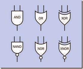
While conventional arithmetic uses arithmetical operators to represent procedures such as addition or multiplication, Boolean algebra uses Boolean operators. The operators of special interest in digital electronics are named AND, NAND, OR, NOR, XOR, and XNOR.

Although each gate actually contains multiple transistors, it is represented by a single logic sym- bol, as shown in Figure 10-1. The names of the Boolean operators are customarily printed all in caps. A gate requires a power supply and a connection with negative ground, separate from its inputs, but these connections are omitted from

gate schematics because they are assumed to exist.
clip_image005

Figure 10-1. Six types of two-input logic gates are used in digital electronics, although the XNOR gate is rare, as it has few applications. The names are customarily printed in uppercase letters.

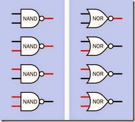
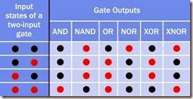
The functions of the gates with two inputs can be defined in electrical terms. In Figure 10-2, the four possible combinations of inputs are tabula- ted in the left column, with red indicating a high input and black indicating a low input. The corresponding output from each gate is shown beneath its name. This kind of tabulation is known as a truth table, as it is derived from Boolean algebra which originally concerned itself with “true” and “false” states.
clip_image007

Figure 10-2. The four possible combinations of input states in a 2-input logic gate are shown at left. The corresponding output from each gate is shown beneath its name. Red indicates a high state, while black indicates a low state.

The truth table assumes that positive logic is being used. Negative logic is very uncommon, but if it were used, the red dots in the truth table would correspond with low inputs and outputs, while the black dots would correspond with high inputs and outputs.

Inversion

The small circles appended to the outputs of NAND, NOR, and XNOR gates mean that the out- put of each gate is inverted compared with the AND, OR, and XOR gates. This can be seen by in- spection of the output states shown in Figure 10-2. The circles are known as bubbles.

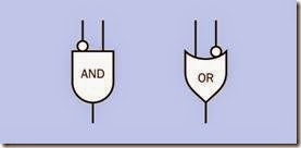
Sometimes logic symbols are shown with a bub- ble applied to one input, as in Figure 10-3. In these cases, the circle indicates that an input must be inverted. More than one gate may be needed to achieve this logic function in an actual circuit. The style is often used to show the inner workings of an IC, using a minimum number of logic symbols.
clip_image009

Figure 10-3. The circle in a logic gate symbol indicates that a signal is being inverted. Circles can be inserted at gate inputs, but in a real circuit a separate inverter is likely to be needed to create this effect.

Single-Input Gates

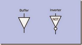
Two gates exist that have a single input and a single output, shown in Figure 10-4. The buffer should not be confused with the symbol for an op-amp or a comparator. (Those components always have two inputs.) The output state of a buffer is the same as its input state, but the component may be useful to deliver more current or to isolate one section of a circuit from another.

When a bubble is appended to a buffer, it be- comes a NOT gate, more commonly known as an inverter. Its function is to create an output state that is opposite to its input state.
clip_image011

Figure 10-4. The two logic gates that have only one input and one output. Note that in some schematics showing internal logic of ICs, the bubble on an inverter may be found on the input side instead of the output side.

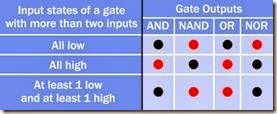
Gates with More than Two Inputs AND, NAND, OR, and NOR gates can have any number of inputs, as suggested in Figure 10-5, although practical factors usually limit the inputs

to a maximum of eight.
clip_image013

Figure 10-5. The previous table has been modified to show the outputs from logic gates that have more than two inputs. XOR and XNOR gates are not included in the table, because a strict interpretation of their logic requires that a unique output state exists if one input is high while the other is low.

The rules can be summarized like this:

• Output from an AND gate: Low if any of its inputs is low, high if all of its inputs are high.

• Output from a NAND gate: High if any of its inputs is low, low if all of its inputs are high.

• Output from an OR gate: High if any of its inputs is high, low if all of its inputs are low.

• Output from a NOR gate: Low if any of its in- puts is high, high if all of its inputs are low.

In the case of XOR and XNOR gates, their logic requires that a unique output state must exist if one input is high while the other input is low.

In fact, so-called three-input XOR gates do exist, an example being the 74LVC1G386 chip, in which the output is high if all three inputs are high, or if one input is high, but not if two inputs are high or no inputs are high. Further discussion of more- than-two-input XORs is outside the scope of this encyclopedia.

Boolean Notation

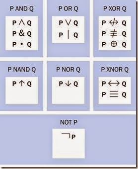
For reference, the original written notation for Boolean operators is shown in Figure 10-6. Un- fortunately, the notation for these operators was never properly standardized, and in more than one instance, multiple symbols acquired the same meaning. The letters P and Q are often, but not always, used to represent two input states that can be true or false.

• The use of a horizontal line above a symbol, to indicate that its state has been reversed, has carried over to datasheets where this notation can show that an output state from any digital chip is inverted. The line is known as a bar.

Arithmetical Operations

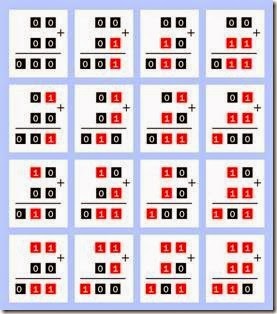
Suppose we wish to sum two binary numbers, each containing two digits. There are four digits altogether, and depending on their values, there are 16 different possible addition sums, as shown in Figure 10-7.

If A0 and B0 represent the rightmost digits of the two numbers being added, and S0 is the sum of those two digits, inspection of the figure shows that the sum can be derived using just three rules:

1. If A0 = 0 and B0 = 0, then S = 0.

2. If A0 and B0 have opposite states, then S0 = 1.

3. If A0 = 1 and B0 = 1, then S0 = 0, and carry 1 to the next place left.

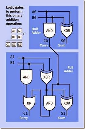
If A0 and B0 are the two inputs to an XOR logic gate, the output of the gate satisfies all three rules, except the need to carry 1 to the next place left. This last function can be satisfied with an AND gate. The function of two gates is known as a half adder, and is shown in the top section of Figure 10-8.
clip_image015

Figure 10-6. Boolean operators as they have been ex- pressed in written notation. Lack of standardization has resulted in more than one symbol representing some of the operators.

When we consider the next pair of binary digits to the left, the situation now becomes more complicated, because we may be carrying 1 into this addition sum from the previous stage, and we still need to be able to to carry 1 out (if necessary) to the next stage. An assembly of five logic gates can deal with this, and their combination is known as a full adder. This is shown in the bottom section of Figure 10-8.
clip_image017

Figure 10-7. Sixteen different addition sums are possible, when summing two binary numbers of two digits each.

The combination of XOR and AND gates shown in Figure 10-8 is not the only one that works to add binary numbers. However, it may be the most intuitively obvious.

Other Operations

Binary arithmetic remains the most important application of logic gates, but individually pack- aged gates are seldom used for that purpose anymore. They were long since subsumed into large multifunction computing chips.

Single gates still have application in small systems, or to modify the inputs and outputs of microcontrollers, or to convert the output from one complex digital chip to make it compatible with the input of another. This last application is often referred to as glue logic.

Applications for single gates are discussed in “How to Use It” on page 103.
clip_image019

Figure 10-8. Logic gates can be used to add binary numbers, using a high input or output to represent a binary 1 and a low input or output to represent a binary 0. This schematic shows one possible way for gates to add two two-digit binary numbers.

Variants

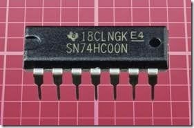
Chips containing logic gates were introduced in the 1960s. The 7400 NAND chip, from Texas In- struments, was the first of a series that became so influential, the same basic part numbers (with letters added before, after, and among the digits) are still used today. An example of a currently available through-hole 7400 chip is shown in Figure 10-9.
clip_image022

Figure 10-9. A modern version of a 7400 chip containing four NAND gates.

Initially, these chips conformed with a transistor- transistor logic (TTL) standard that had been invented at TRW in 1961 and introduced in commercial products by Sylvania in 1963. It established the now-familiar standard of 5VDC for the power supply. Many logic chips now use other voltages, but the term “high” still means an input or output that is near to the supply voltage, while “low” means an input or output that is near to negative ground. The exact definition of “near” will be found in datasheets for the chips.

The 7400 series was successful partly because it was engineered for compatibility. The output from one gate could be connected directly to the input of another gate, with a few bypass capacitors added on a circuit board to suppress voltage spikes caused by rapid switching. Earlier components had not been so easy to interface with each other. The new standard dominated the industry to the point where dozens of manufacturers started making chips that conformed with it, and a single board could mix-and-match chips from multiple vendors.

Because many logic chips acquired part numbers that began with 74, they are often referred to as the 74xx series, where other digits (sometimes more than two) can be substituted for xx. This avoids ambiguity, as the very first chip in this for- mat was a NAND gate that had 7400 as its actual part number. In the text below, 7400 will refer to that specific chip, whereas 74xx will refer to the whole series of chips.

RCA introduced a competing family of logic gates in 1968, using CMOS transistors. As each part number began with a 4 and contained four digits, this was referred to as the 4000 series. The CMOS chips were slower and more expensive, but tolerated a wider range of power supply voltages (3V to 12V, initially). Their biggest advantage was that they used much less current. This was important, as TTL chips created a lot of waste heat. The lower power consumption of CMOS al- so enabled one chip to control the inputs of many others, which simplified circuit design. This one- to-many relationship is known as fanout.

Ultimately, CMOS chips transcended their early limitations. While they were reserved initially for battery-powered devices in which very low power consumption was more important than speed, CMOS is now used almost everywhere, still maintaining its advantage of low current (almost zero, in fact, while a chip is quiescent) while equalling the speed of TTL. However, CMOS logic chips are very often pin-compatible with the old TTL components, and modern CMOS part numbers are often derived from the old 74xx series.

Most CMOS logic chips in the old 4000 series are still available, and may be used in situations where a power supply greater than 5VDC is convenient.

Part Numbers

As the performance of semiconductors gradually improved, successive families of logic chips were introduced, identified by one-letter, two-letter, or three-letter acronyms. The acronym was inserted into the part number, so that a 7400 NAND gate in the HC (high-speed CMOS) family be- came a 74HC00 NAND gate.

Because these chips were available from multiple sources, the part number was also preceded with one or more letters indicating the manufacturer. And because each chip was manufactured in different versions (for example, some complied

with military specifications, while others didn’t), letters were also appended to the end of the part number. Today, the appended letters may indicate whether the chip is of the old through-hole format, or conforms with a more recent surface- mount format.

Summing up:

• Prefix: manufacturer ID.

• Numerals, omitting any letters in the middle: Chip functionality.

• Middle letters: Chip family.

• Suffix letters: Package format.

Thus, for example, the actual part number for a 74HC00 NAND chip could be SN74HC00N, where the SN prefix indicates that it is manufactured by Texas Instruments and the N suffix means that it is in plastic dual-inline-pin (DIP) format. (The SN prefix was introduced by Texas Instruments in the earliest days of integrated circuits as an acronym for “semiconductor network,” meaning that multiple transistors were “networked” on a wafer of silicon. Other manufacturers used their own schemes for part numbering, and so SN be- came exclusively identified with Texas Instru- ments.)

The system of augmenting part numbers has been further extended by inserting 1G, 2G, or 3G immediately after the family identifier, to indicate surface-mount chips that contain one, two, or three logic gates. If the “G” identifier is missing, the chip usually has four logic gates, which was the standard used in the original 74xx series. This rule applies even in surface-mount formats, where the surface-mount pads of four-gate chips have the same functions as the pinouts of the original TTL versions (except in the case of square-format surface-mount chips, which are not discussed here).

When searching a catalog to find a chip by its part number, it helps to remember that searching for a 7400 chip may not find any hits, but searching for a 74HC00 (or any other valid number containing a family identifier) is much more likely to be understood.

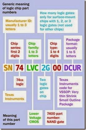
A key to understanding part numbers is shown in Figure 10-10. The upper part of the figure is a guide to interpreting numbers on a generic basis, while the lower part interprets the specific part number shown.

Families

As of 2013, the HC family in the 74xx series has become so widely used, it can be considered the default in the traditional DIP 14-pin format. In- cremental improvements are still being made, and new families are being introduced, primarily in surface-mount formats which use lower power-supply voltages (down to around 1VDC).
clip_image024

Figure 10-10. How to interpret the segments of a logic chip part number in the 74xx family (in this case, a 7400 NAND gate).

Here is an historical summary of the most important chip families.

• 74xx: Original series of bipolar TTL chips.

• 74Hxx: Bipolar TTL, high speed, about twice as fast as the original 74xx chips, but twice the power consumption.

• 74Lxx: Bipolar TTL, lower power consumption than the original TTL, but also much lower speed.

• 74LSxx: Bipolar TTL, lower power with Schottky input stages, faster than original TTL. Some LS chips are still being manufactured.

• 74ASxx: Bipolar TTL, Advanced Schottky, in- tended to supercede the 74Lxx.

• 74ALSxx: Bipolar TTL, Advanced Low Power Schottky, intended to supercede the 74LSxx.

• 74Fxx: Bipolar TTL, Faster.

• 74HCxx: CMOS high-speed emulation of 74LSxx.

• 74HCTxx: CMOS but with similar high-state input voltage threshold to bipolar TTL chips, for compatibility.

• 74ACxx: Advanced CMOS.

• 74ACTxx: Advanced CMOS emulation of TTL with similar high-state input voltage thresh- old to TTL, for compatibility.

• 74AHCxx: Advanced Higher-Speed CMOS, three times as fast as HC.

• 74VHCxx: Very High Speed CMOS.

• 74AUCxx, 74FCxx, 74LCXxx, 74LVCxx,

74ALVCxx, 74LVQxx, 74LVXxx: Various specifications, many using power supply voltag- es of 3.3V or below.

In the 4000 series, an early significant improvement was the 4000B family, which allowed a higher power supply limit (18V instead of 12V) and was much less susceptible to damage by static discharge. The 4000B family almost totally replaced the old 4000 family, and most 4000B

chips are still available, as they are useful in situations where a power supply delivers more than 5VDC.

• When it is referenced casually, the B at the end of a chip number in the 4000 series may be omitted. When the number is listed in a catalog, the B is included.

Chips with 45 as their first two digits were introduced as a new generation, but were not widely adopted. After that, the 4000 series ceased to evolve, and CMOS chips adopted 74xx part numbers, distinguishing themselves by the insertion of letter groups in the center of the number.

To add to the confusion, some 4000 series part numbers were appended to 74xx part numbers, so that, for example, the 74HCT4060 is designed to be compatible with the old 4060B chip.

Family Interoperability

One of the most important issues relating to chip families is their differing specifications for a low- state voltage and a high-state voltage in inputs and outputs.

The original 74xx TTL series, using a 5VDC power supply, used these approximate specifications:

• Output: 74xx voltage representing a low state (at most 0.4V to 0.5V)

• Input: 74xx input voltage interpreted as a low state (maximum 0.8V)

• Output: 74xx voltage representing a high state (at least 2.4V to 2.7V)

• Input: 74xx input voltage interpreted as a high state (minimum 2V)

This provided a safe margin of error of at least 0.4V when chips were communicating with each other.

In the CMOS 4000 family, however, logic chips required a minimum input of 3V to 3.5V to be interpreted as a high state. The minimum acceptable output from a TTL chip was below this level, creating problems if anyone should try to use the output from a TTL chip to communicate with an input on a CMOS chip.

One solution is to add a 4.7K pullup resistor to the TTL output, guaranteeing that it won’t fall too low. But this wastes power, and the need for the resistor is easily forgotten. Another option is to use the HCT or ACT family of CMOS logic. The “T” in these family names indicates that they have been engineered to share the input standards of the old TTL chips. They still deliver the same high output as other types of CMOS, making them seem to be the best possible solution. Unfortunately, it does entail a compromise: the “T” chips are more sensitive to noise, among other factors.

• Ideally, chip families should not be intermingled.

Gates per Chip

Each of the original 74xx chips contained multiple gates within the limits of a uniform 14-pin through-hole format. The gates that were most commonly used had two inputs, and there were four of these gates per chip.

However, the desire for miniaturization, and the use of automatic chip-placement and soldering equipment, made one-gate and two-gate logic chips desirable and practical in surface-mount format. (Three-gate surface-mount chips exist, but are sufficiently unusual that they are not de- scribed in this encyclopedia.)

Two Inputs, Single Gate

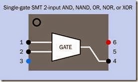
Where a chip contains just one logic gate, it is almost always a surface-mount component, and the part number has 1G in the middle to indicate “one gate.” Pad functions are shown in Figure 10-11. The layout is standardized for all logic gates, with the exception of XNOR gates, which are not manufactured in surface-mount format.
clip_image026

Figure 10-11. Internal configuration and solder-pad functions for a two-input surface-mount single-gate logic chip that can contain an AND, NAND, OR, NOR, or XOR gate. XNOR gates are not manufactured in this format.

In the figure, a gate is shown in generic form, indicating that it may be an AND, NAND, OR, NOR, or XOR gate, depending on the part number of the chip. Inputs are on the left of the gate, while its output is on the right. The chip does not have a solder pad in position 5, but the pad at top right is identified as pin 6 for consistency with the numbering pattern in other surface-mount components where six pads are common.

The generic part numbers for single-gate surface-mount two-input logic chips are shown here, with letter x indicating that letter sequences are likely to be inserted to indicate manufac- turer, logic family, and chip format:

• AND gate: x74x1G08x

• OR gate: x74x1G32x

• NAND gate: x74x1G00x

• NOR gate: x74x1G02x

• XOR gate: x74x1G86x

Three Inputs, Single Gate

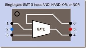
AND, NAND, OR, and NOR single gates are avail- able with more than two inputs. Their output is determined by rules shown in Figure 10-5. XOR and XNOR gates are not included in the table, because a strict interpretation of their logic re- quires that a unique output state exists if one in- put is high while the other is low.

The pad functions for a surface-mount single- gate logic chip with three inputs are shown in Figure 10-12. The generic part numbers for these chips are shown below. Again, each x indicates that letter sequences are likely to be inserted to indicate manufacturer, logic family, and chip format.
clip_image028

Figure 10-12. Internal configuration and solder-pad func- tions for a three-input surface-mount single-gate logic chip that can contain an AND, NAND, OR, or NOR gate.

The generic part numbers for single-gate surface-mount three-input logic chips are shown here, with each x indicating that letter se- quences are likely to be inserted to indicate man- ufacturer, logic family, and chip format:

• AND: x74x1G11x

• NAND: x74x1G10x

• OR: x74x1G32x

• NOR: x74x1G27x

Single Gate, Selectable Function

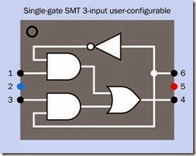
A few surface-mount chips can emulate a variety of two-input gates, by using appropriate external connections. The internal logic of one example, with generic part number x74x1G97x (an actual example would be Texas Instruments SN74LVC1G97), is shown in Figure 10-13. De- pending which pin is grounded and which other pins are used as inputs, the chip can emulate all five of the most commonly used gates. To achieve this, however, some inputs have to be inverted.
clip_image030

Figure 10-13. Internal configuration for a configurable surface-mount chip that can emulate various two-input logic gates, depending which inputs are used and which are grounded. Some inputs have to be inverted to emulate some gates.

Two Inputs, Dual Gate

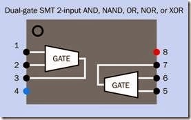
Two-input surface-mount AND, NAND, OR, NOR, and XOR gates are available in dual layout (two gates per chip). The internal logic and pad functions are shown in Figure 10-14. The generic part numbers for these chips are shown here. Again, each x indicates that letter sequences are likely to be inserted to indicate manufacturer, logic family, and chip format.
clip_image032

Figure 10-14. Internal configuration and solder-pad functions for a two-input surface-mount dual-gate logic chip that can contain two AND, NAND, OR, NOR, or XOR gates. XNOR chips are not manufactured in this format.

The generic part numbers for dual-gate surface- mount two-input logic chips are shown below, with each x indicating that letter sequences are likely to be inserted to indicate manufacturer, logic family, and chip format:

• AND: x74x2G08x

• NAND: x74x2G00x

• OR: x74x2G32x

• NOR: x74x2G02x

• XOR: x74x2G86x

Original 74xx 14-Pin Format

Each of the original 74xx TTL chips contained multiple gates within the limits of a uniform 14- pin chip format. The available options were, and still are:

• Quad 2-input: Four gates with two inputs each

• Triple 3-input: Three gates with three inputs each

• Dual 4-input: Two gates with four inputs each

• Dual 5-input: Two gates with five inputs each

• Single 8-input: One gate with eight inputs

The five-input chips have become so uncommon that they are not described in this encyclopedia.

Quad Two-Input 74xx Pinouts

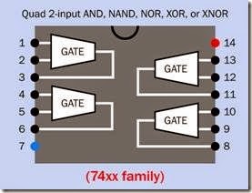
14- pin DIP 74xx quad two-input logic chips are available in AND, NAND, NOR, XOR, or XNOR ver- sions, all of which have an internal layout shown in Figure 10-15. The layout is unchanged in surface-mount format. The gates are shown in generic form, as the layout remains the same re- gardless of which type of gate is in the chip. All the gates in any one chip are of the same type. The four connections leading to a gate are its in- puts, while the single connection from a gate is its output.
clip_image034

Figure 10-15. In a 14-pin quad two-input 74xx logic chip, the AND, NAND, NOR, XOR, and XNOR versions all share this generic layout.

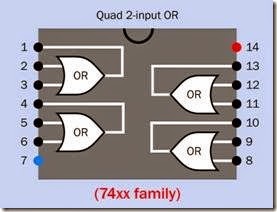
• The 14-pin quad two-input OR chip has different pinouts from all the other 74xx logic chips. It is shown in Figure 10-16.
clip_image036

Figure 10-16. In a quad two-input 74xx OR chip, this lay- out is used, which is different from that used in all the other quad two-input logic gates.

Triple Three-Input 74xx Pinouts

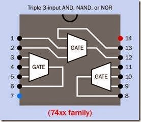
The AND, NAND, and NOR versions of a 14-pin DIP 74xx triple three-input logic chip all have an internal layout shown in Figure 10-17. The layout is unchanged in surface-mount format. The gates are shown in generic form, as the layout remains the same regardless of which type of gate is in the chip. All the gates in any one chip are of the same type. Three connections leading to a gate are its inputs, while a single connection from a gate is its output.
clip_image038

Figure 10-17. In a 14-pin triple three-input 74xx logic chip, the AND, NAND, and NOR versions all share this generic layout.

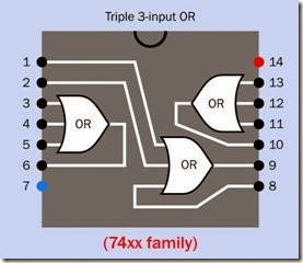
– The 14-pin triple three-input OR chip has different pinouts from all the other 74xx logic chips. It is shown in Figure 10-18.
clip_image040

Figure 10-18. In a triple three-input 74xx OR chip, this lay- out is used, which is different from that used for all the other triple three-input logic gates.

Dual Four-Input 74xx Pinouts

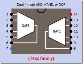
A 14-pin DIP 74xx dual four-input logic chip con- tains two four-input gates. The AND, NAND, and NOR versions all have an internal layout shown in Figure 10-19. The layout is unchanged in surface-mount format. The gates are shown in generic form, as the layout remains the same regardless of which type of gate is in the chip. All the gates in any one chip are of the same type.

• There is no OR chip of the 14-pin dual four- input type.
clip_image042

Figure 10-19. In a 14-pin dual four-input 74xx logic chip, the AND, NAND, and NOR versions all share this generic layout. There is no 74xx OR chip with four inputs per gate.

Single Eight-Input 74xx Pinouts

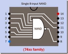
A 14-pin DIP 74xx single eight-input NAND chip contains one eight-input gate, as shown in Figure 10-20. The layout is unchanged in surface- mount format.

• There is no AND chip of the 14-pin single eight-input type.

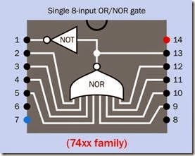
A 14-pin eight-input logic chip in the 74xx series, able to function as both an OR and a NOR, is shown in Figure 10-21. The output from the NOR gate is connected with pin 13, but also passes through an inverter to create an OR output at pin

1. (Because a NOR gate is equivalent to an

inverted-OR, when its output is inverted again, it returns to being an OR.)
clip_image044

Figure 10-20. The internal layout of single eight-input NAND chip in the 14-pin 74xx series. There is no 74xx AND chip with eight inputs per gate.
clip_image046

Figure 10-21. The internal layout of single eight-input OR/NOR chip in the 14-pin 74xx series. Pin 13 has the NOR output, while pin 1 has the OR output.

The following list shows the generic part numbers for DIP and surface-mount versions of 14- pin logic chips in the 74xx series that have two or more inputs per gate. As before, an x indicates that letter sequences are likely to be inserted to indicate manufacturer, logic family, and chip format.

• Quad 2-input AND: x74x08x

• Quad 2-input NAND: x74x00x

• Quad 2-input OR: x74x32x

• Quad 2-input NOR: x74x02x

• Quad 2-input XOR: x74x86x

• Quad 2-input XNOR: x74x266x

• Triple 3-input AND: x74x11x

• Triple 3-input NAND: x74x10x

• Triple 3-input OR: x74x4075x

• Triple 3-input NOR: x74x27x

• Dual 4-input AND: x74x21x

• Dual 4-input NAND: x74x20x

• Dual 4-input NOR: x74x4002x

• Single 8-input NAND: x74x30x

• Single 8-input OR/NOR: x74x4078x

74xx Inverters

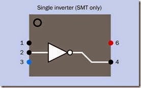
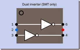
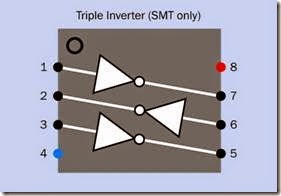
Single, dual, and triple inverter packages in the 74xx series are available in surface-mount format only. Their internal arrangement is shown in Fig- ures 10-22, 10-23, and 10-24.
clip_image052

Figure 10-22. The internal layout of a 74xx series logic chip containing one inverter. This is available in surface- mount format only. Pin 5 is absent. Pin 1 is not connected.
clip_image050

Figure 10-23. The internal layout of a 74xx series logic chip containing two inverters. This is available in surface- mount format only.
clip_image048

Figure 10-24. The internal layout of a 74xx series logic chip containing three inverters. This is available in surface-mount format only.

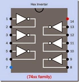
In the 14-pin format, a hex inverter chip (con- taining six inverters) is available, as shown in Figure 10-25. The layout is the same for DIP and surface-mount formats.

Generic part numbers for inverter chips are as follows:

• Single inverter: x74x1G04x

• Dual inverter: x74x2G04x

• Triple inverter: x74x3G14x

• Hex inverter: x74x04x
clip_image054

Figure 10-25. The internal layout of a 14-pin 74xx hex in- verter logic chip, containing six inverters. This layout is the same for DIP and surface-mount versions.

Additional Variations

Some chips in the 74xx series (both DIP and sur- face mount versions) have variants with open drain or open collector outputs, while others have inputs that are configured as Schmitt triggers. These variants will be found as hits when searching supplier websites for logic chips by gate name and number of inputs.

Pinouts in the Original 4000 Series

Each of the original 4000 CMOS chips contained multiple gates within the limits of a uniform 14- pin chip format. The available options were, and still are:

• Quad 2-input: Four gates of two inputs each

• Triple 3-input: Three gates of three inputs each

• Dual 4-input: Two gates of four inputs each

• Single 8-input: One gate of eight inputs

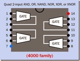
In the 4000 family, 14-pin quad two-input logic chips are available in AND, OR, NAND, NOR, XOR, or XNOR versions, all of which have an internal layout shown in Figure 10-26. The gates are shown in generic form, as the layout remains the same regardless of which type of gate is in the chip. All the gates in any one chip are of the same type. The four connections leading to a gate are its inputs, while the single connection from a gate is its output.

Unlike the 74xx family, the quad two-input OR chip in the 4000 family has the same pinouts as the other types of quad two-input logic chips.
clip_image056

Figure 10-26. In the 4000 family, the AND, OR, NAND, NOR, XOR, and XNOR versions of a quad two-input logic chip all share this generic layout.

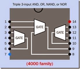
In the 4000 family, a 14-pin triple three-input logic chip contains three three-input gates. The AND, OR, NAND, and NOR versions all have an internal layout shown in Figure 10-27. The gates are shown in generic form, as the layout remains the same regardless of which type of gate is in the chip. All the gates in any one chip are of the same type. The three connections leading to a gate are its inputs, while a single connection from a gate is its output.

Unlike the 74xx family, the triple three-input OR chip in the 4000 family has the same pinouts as the other types of triple three-input logic chips.

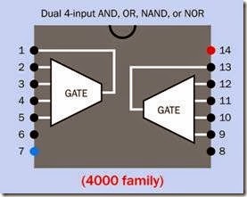
In the 4000 family, a 14-pin dual four-input logic chip contains two four-input gates. The AND, NAND, OR, and NOR versions all have an internal

layout shown in Figure 10-28. The gates are shown in generic form, as the layout remains the same regardless of which type of gate is in the chip. All the gates in any one chip are of the same type. Each pair of connections leading to a gate are its inputs, while the single connection from a gate is its output.
clip_image058

Figure 10-27. In the 4000 family, the AND, OR, NAND, and NOR versions of a triple three-input logic chip all share this generic layout.

Note that the 4000 family does have a dual four- input OR chip, whereas the 74xx family does not.

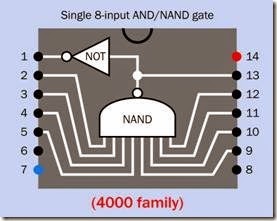
In the 4000 family, a 14-pin eight-input logic chip with AND and NAND outputs is available, as shown in Figure 10-29.

The following list shows the generic part num- bers for 14-pin logic chips in the 4000 family that have two or more inputs per gate (in actual part numbers, letters will be substituted where an x appears):

• Quad 2-input AND: x4081x

• Quad 2-input NAND: x4011x

• Quad 2-input OR: x4071x

• Quad 2-input NOR: x4001x

• Quad 2-input XOR: x4070x

• Quad 2-input XNOR: x4077x

• Triple 3-input AND: x4073x

• Triple 3-input NAND: x4023x

• Triple 3-input OR: x4075x

• Triple 3-input NOR: x4025x

• Dual 4-input AND: x4082x

• Dual 4-input NAND: x4012x

• Dual 4-input OR: x4072x

• Dual 4-input NOR: x4002x

• Single 8-input AND/NAND: x4068x
clip_image060

Figure 10-28. In the 4000 family, the AND, OR, NAND, and NOR versions of a dual four-input logic chip all share this generic layout.

4000 Series Inverters

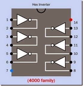
In the 4000 family, the 4069B is a 14-pin hex inverter chip (containing six inverters), as shown in Figure 10-30. This has the same pinouts as the x74x04x chip.

How to Use It
Which Family

In DIP format, the HC family has existed for more than 30 years, and has become established as a widely used default choice.

In surface-mount formats, the choice of family will largely be determined by the choice of sup- ply voltage.
clip_image063

Figure 10-29. In the 4000 family, a single eight-input AND/NAND chip has this internal layout. The inverted output from the NAND gate becomes an AND output from pin 1 of the chip.
clip_image065

Figure 10-30. The internal layout of a 14-pin 4069B hex inverter logic chip, containing six inverters. This layout is the same as for the x74x04x chip.

Although the 4000 series is now more than 40 years old, it may still be useful where a 5VDC power supply is not required for other reasons in a circuit and would be added purely to power a 74xx series logic gate or other digital chip. If a circuit contains a 9VDC or 12VDC relay, for in- stance, a Darlington pair may be used with that voltage to drive the relay, and an old-school 4000 series logic chip could share the same supply. The relay coil would need a clamping diode to pro- tect the logic chip from transients.

Applications

The output from a logic chip may be used as an input for a microcontroller, to enable multiple inputs to share one pin. An eight-input NAND gate, for instance, could combine the inputs from eight normally on motion sensors. If just one sensor responds to an intrusion, the gate output would change from high to low.

Logic gates may be useful in any simple device that has to respond to a single, specific combination of inputs. A digital combination lock is one example; games of chance are another. Most simple dice simulations use logic gates to convert the output from a counter to drive a dice- pattern of LEDs.

A logic gate may be used as an interface between an electromechanical switch and a circuit containing digital chips. A 10K pullup or pulldown resistor prevents the gate input from floating when the switch is open. A buffer can be used for this purpose, or an inverter, or any “spare” gate on a logic chip that is already in the circuit. One input of the chip can be tied to the positive power supply or negative ground, to create an appropriate input from the chip when the switch, attached to the other input, is opened or losed.

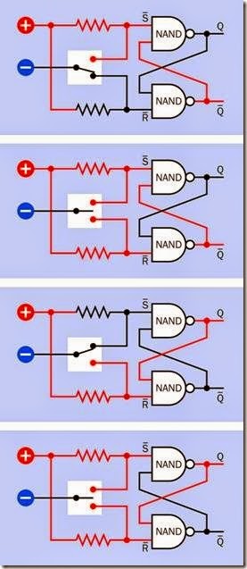
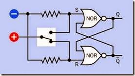
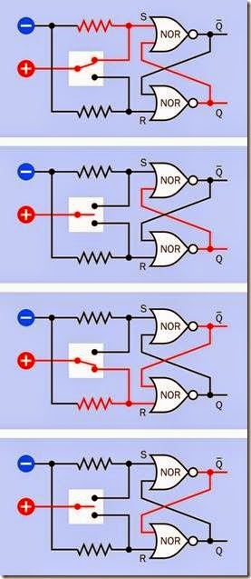
A jam-type flip-flop can be used to debounce a switch input. See Chapter 11 for details. If two NOR or two NAND gates are unused in a circuit, they can form a flip-flop.

In the original CMOS 4000 family, a positive out- put may be capable of driving an LED if the cur- rent does not exceed 5mA with a power supply of 5VDC or 10mA with a power supply of 10VDC. Note that the output voltage will be pulled down significantly by these loads. In the 74HCxx family, chips can source or sink as much as 20mA, but here again the output voltage will be pulled down. Note that the total limit for all outputs from a 74HCxx chip is around 70mA.

The output from a logic chip can be passed through a buffer such as the 7407, which has an open-collector output capable of sinking as much as 200mA. This enables direct drive of modest loads, so long as they are not inductive.

Solid-state relays and optocouplers can be driven directly from logic chips, as they draw very little current. A solid-state relay can switch 50A or more.

What Can Go Wrong

Two problems are common when using CMOS digital chips: damage from static electricity, and erratic behavior caused by floating pins.

Static

The early 4000 series CMOS chips were especially vulnerable, but more recent CMOS designs generally include diodes at the inputs, which reduces the risk. Still, logic chips should be protected by inserting them into anti-static foam or enclosing them in conductive wrappers until they are in- stalled in a board. While handling chips, it is good practice to be grounded, ideally using a wrist- mounted ground wire.

Floating Pins

Any pin which is unconnected in a logic chip is considered to be “floating,” and can pick up signals by capacitive coupling, possibly disrupting the behavior of the chip and also causing power consumption, as the ambiguous pin state will tend to prevent that gate in the chip from enter- ing quiescent mode.

Generally speaking, input pins in a TTL logic chip that are not being used for any purpose should be tied to the positive voltage supply, while un- used CMOS pins should be tied to negative ground.

Family Incompatibilities

As previously noted, older TTL logic chips may deliver a “high” output voltage that is lower than the minimum expected by newer CMOS logic chips. The best option is not to mix families, but if chips are stored carelessly, some intermingling can occur. Part numbers should be checked if one chip appears to be ignoring output from another.

Overloaded Outputs

If a circuit calls for a logic chip with an open- collector output, and a regular chip is used by mistake, it will almost certainly be damaged.

Output Pulled Down

If the output from one logic chip is connected with the input of another logic chip, and if the output from the first chip is also connected to an LED, the LED may pull down the output voltage so that the second chip will not recognize it as a high state. As a general rule, a logic output can drive an LED, or can drive another logic chip, but not both. Very-low-current LEDs, which draw as little as 2mA, may be acceptable.

Incorrect Polarity and Voltages Logic chips can be knocked out by applying in- correct polarity, or voltage to the wrong pin, or the wrong voltage. Modern logic chips tolerate a very limited voltage range, and a 74xx series chip will be irrevocably damaged if it is used where a 4000 series chip was specified for a power supply higher than 6VDC.

If a chip is inserted upside-down, it will probably be damaged when voltage is applied.

Bent Pins

Like all through-hole chips, DIP logic chips can be inserted accidentally with one or more pins bent underneath the chip. This error is very easy to miss. The bent pins will not make contact with any socket that is used, and the chip will behave unpredictably. Check for proper pin insertion with a magnifying glass if necessary.

Unclean Input

Logic chips expect a clean input without voltage spikes. A 555 timer of TTL type generates spikes in its output which can be misinterpreted as multiple pulses by the input of a logic chip. A CMOS- type 555 timer is more suitable for connection with logic chips.

If a pushbutton, rotational encoder, or electro- mechanical switch provides a high or low input, the input must be debounced. In hardware, this is traditionally done with a flip-flop. It can also be done with code in a microcontroller.

Analog Input

The input of a logic chip can be connected directly with a thermistor, phototransistor, or similar analog component, but only if there is some certainty that the voltage at the input pin will remain within the range that is acceptable to the chip. In the case of a phototransistor, for example, it should be exposed to a limited, known range of light intensity.

In general, it is best to avoid applying intermediate-voltage signals to a digital logic input, as they can create unpredictable output, or output of an intermediate voltage. A comparator can be placed between the analog source and the digital logic chip, or a logic chip with a Schmitt-trigger input can be used.
 

shift register:What It Does,Schematic Representation,How It Works,Abbreviations and Acronyms,Parallel Outputs and Inputs,Variants,Serial In, Serial Out,Serial In, Parallel Out,Parallel In, Serial Out,Parallel In, Parallel Out and Universal.

shift register

The term shift register is rarely hyphenated. In this encyclopedia, no hyphen is used.

A shift register can function as a queue, but this term is more usually applied to software. When the output from the last stage of a shift register is connected back to its input, it can function as a ring counter, but that application is described in the counter entry of this encyclopedia.

Component catalogs sometimes list shift registers as binary ripple counters, instead of giving them their own section. In this encyclopedia, a binary counter is considered to have binary-weighted outputs (with values 1, 2, 4, 8…. in decimal notation) and is de- scribed in the counter entry. A shift register has outputs that are not necessarily binary- weighted.

What It Does

A register is a component (or a small section of computer memory) that stores information. The smallest unit of information is one bit (i.e., one binary digit) with a value 1 or 0 that can be rep- resented by a high or low logic state. A shift register most commonly is designed to store eight bits, although some store four.

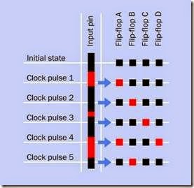
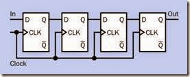
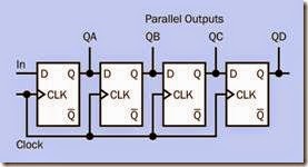
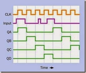
Each bit is memorized by the status of a flip- flop inside the register. For a detailed description of flip-flops, see Chapter 11. When a pulse from an external clock is received by the shift register, all of the bits in storage are moved along one step, from each flip-flop to the next. The high or low status of an input pin at that moment is clocked in to the first flip-flop, while the bit in the last flip-flop is overwritten by the bit preceding it. A diagram representing the function of a basic four-bit shift register is shown in Figure 12-1.

Note that the status of the input pin is ignored until the moment when a clock pulse copies it into the first flip-flop. In the figure, when the in- put pin has a brief high state that ends immediately before clock pulse three, the high state is ignored.

A shift-register chip is shown in Figure 12-2. Because the functionality of a shift register is now often incorporated in much larger logic chips, it is less widely used as a stand-alone component than it used to be. It is still useful for purposes of serial-parallel or parallel-serial conversion, and for small tasks such as scanning a matrix- encoded keyboard or keypad. It also has educational applications and can be used in conjunc- tion with a microcontroller.

clip_image005

Figure 12-1. The function of a four-bit shift register in which each flip-flop may be set to a high or a low state, represented here with red or black squares. After a high bit is clocked into the chip, it is moved one space along by each subsequent clock pulse.

clip_image007

Figure 12-2. This 8-bit shift-register chip is unusual in that it uses “power logic,” in which open-drain outputs en-

gram showing the physical chip and its pinouts. The meaning of the abbreviations identifying the inputs, outputs, and control functions will be de- scribed in “How It Works” on page 122.

clip_image009

Figure 12-3. Typical schematic representation of a shift register, compared with the pinouts of the actual component.

The schematic symbol representing a shift register may appear superficially similar to the phys- ical form of the chip which contains it, but the physical layout of the pins is unlikely to be the same.

How It Works

able it to drive relatively high-current devices. It can sink up to 250mA at each of its output pins, at up to 45VDC.

Schematic Representation

No specific symbol exists for a shift register. It is represented in a schematic by a simple rectangle, often (but not always) with control inputs on the left, data inputs arrayed along the upper edge, and data outputs along the lower edge. An ex- ample is shown in Figure 12-3, along with a dia- A shift register generally consists of a chain of D- type flip-flops. See the entry describing flip-flops in Chapter 11 for a detailed explanation of this component.

The simplest shift register functions as a serial-in, serial-out device, abbreviated with the acronym SISO. Because the first bit that enters it will be the first to leave at the opposite end, it can also be described as a first-in, first-out data storage de- vice, using the acronym FIFO.

The basic connections between flip-flops in a four-bit SISO shift-register are shown in Figure 12-4. The D input in each section refers to the fact that it is a D-type flip-flop. The primary output from each flip-flop is identified with letter Q.

clip_image011

Figure 12-4. The simplest shift register is a serial-in, serial-out (SISO) device. This example contains four D- type flip-flops.

Each clock input is labeled CLK. When the output of each flip-flop is coupled to the input of the next flip-flop, and both share the same clock signal, the clock signal will cause the state of the third flip-flop to be sent to the fourth, the output of the second to be copied to the third, the out- put of the first to the second, and the input state will be copied to the first.

Abbreviations and Acronyms

The shift register will usually have an additional input that forces an immediate “clear” of all the registers, regardless of the clock state at that mo- ment. This input is usually labeled CLR and will have a bar printed above it if it is active-low (which is the usual convention). If there is a pin labeled MR (meaning “Master Reset”), it will have the same function as CLR.

Because its effect is independent of the clock state, the clear signal is described as an asynchronous input.

While the abbreviation CLK is frequently used to identify the clock input, SCLK is also used (meaning “serial clock”), and occasionally the abbreviation CP may be found, meaning “clock pulse”

input. If the shift register contains two stages, one to clock data in and the second to clock data out, they may be separately clocked, in which case they will be identified with different abbreviations. These are not standardized, but should be explained in the manufacturer’s datasheet. No matter which abbreviation is used for a clock input, it will have a bar printed above it if the in- put is active-low.

Shift registers are generally edge triggered, meaning that the rising or falling edge of a clock pulse triggers the bit-shifting operation. If the component responds to a clock transition from low to high, it is rising-edge triggered. If it responds to a transition from high to low, it is falling-edge triggered, and this may be indicated in the schematic by a small circle, properly known as a bubble, preceding the triangle which indicates that this is an edge-triggered device.

Most shift registers are positive-edge triggered.

Parallel Outputs and Inputs

In many shift registers, data may be read out in parallel (from all flip-flops simultaneously), using pins provided for this purpose. In this mode, the shift register can function as a serial-parallel con- verter (serial in, parallel out, represented by the acronym SIPO). A simplified schematic of the internal connections is shown in Figure 12-5.

Where parallel outputs are provided, they are often identified as QA, QB, QC, and so on (moving from left to right) but may alternatively be de- scribed as Q1, Q2, Q3, Q4, and so on.

In a schematic, the input pin is conventionally shown as being at the left end of the component. Often two inputs are provided, connected inter- nally as inputs to a NAND gate. The inputs are likely to be labeled A and B, but may alternatively be named SA and SB, indicating that they are serial inputs. S1 and S2 are alternative classifica- tions. If parallel inputs exist, they may be identified as PA, PB, PC, and so on.

clip_image013

Figure 12-5. Many shift registers have pins connected to points along the chain of flip-flops. These connections en- able data to be read from the shift register in parallel.

If serial data is supplied asynchronously, as in the illustration in Figure 12-1, it will be ignored until the shift register is triggered by the next clock pulse. The input state at that moment will then be copied into the first flip-flop, while the data that is already being stored in the shift register will be moved along the chain. In datasheets, this is customarily represented by a diagram such as the one in Figure 12-6. This diagram assumes that the shift-register is rising-edge triggered. Note that a brief fluctuation in the input which does not coincide with a clock-trigger event will be ignored.

Variants
Serial In, Serial Out

A basic SISO shift register allows only for serial input (at one end of the chain of flip-flops) and serial output (at the other end of the chain). No pins are available for parallel output of data.

This type of component usually permits 64-bit storage, where parallel output is simply impractical, as too many pins would be required. An ex- ample is the 4031B chip. This includes provision for recirculation of bits, so that it will also function as a ring counter (see Chapter 13 for a discussion of this function). As is always the case with logic chips, the part number will be preceded by letter(s) identifying the manufacturer, and a suffix will distinguish variants of the chip.

Another type of SISO shift register is programmable. It will store any number of bits from 1 through 64, determined by a binary number applied in the form of high/low states to five pins reserved for this purpose. An example is the 4557B.

clip_image016

Figure 12-6. In a rising-edge-triggered shift register, the high or low state of an asynchronous input (purple line) is copied into the first flip-flop of a shift register by each clock pulse (orange line). Brief fluctuations that do not coincide with a rising clock pulse are ignored. Existing data in the register is shifted from one flip-flop to the next.

Serial In, Parallel Out

The majority of serial-input shift registers allow parallel output from points along the chain in addition to serial output at the end of the chain. These chips almost all are 8-bit registers. Typically two inputs are provided, one of which can be used to receive bits that recirculate from the end of the chain, back to the beginning. Widely used examples are the 4094B and the 74×164, where an acronym identifying the logic family will be substituted for the x.

Parallel In, Serial Out

A minority of shift registers are able to function as parallel-serial converters (parallel in, serial out, represented by the acronym PISO). Typically this type of chip allows jam-type parallel data input, meaning that the data is forced into the flip-flops

via a separate pin for each of them. Parallel input is enabled by the status of a serial/parallel control pin. When the control pin reverts to its opposite status, each clock pulse will now shift data along the chain of flip-flops, allowing it to be read from the final output one bit at a time. Thus, data can be entered into the chip in parallel and read out of it serially. Examples are the 4014B and 4021B. Both are 8-bit.

Parallel In, Parallel Out

Shift registers that permit parallel output in addition to parallel input are almost all of the universal type, described in the next section.

Universal

A universal shift register is capable of all four modes of operation: SISO, SIPO, PISO, and PIPO. The four modes of the component are selected by the high or low status of two mode select pins. In addition, this component may have the ability to shift the register states either left or right. A bidirectional shift register has this same capabil- ity, and may also have PISO and PIPO capability, depending on the chip. Examples are the 74×195 and 74×299, where an acronym identifying the logic family will be substituted for the x in the number.

Universal shift registers are almost all 4-bit or 8- bit. They often have relatively complicated features, such as access to internal JK flip-flops, or pins that are multiplexed to provide different functionality depending whether an enable pin is held high or low. Datasheets must be checked carefully to ensure correct use.

Dedicated shift registers of SIPO or PISO type will be easier to use.

Values

As is the case with other logic chips, most flip- flops in the through-hole 74xx series are intend- ed for 5VDC power supply while the older 4000 series may tolerate up to 18VDC. Surface-mount versions may use voltages as low as 2VDC.

See the section on logic gates in Chapter 10 for a discussion of acceptable high and low logic- input states. On the output side, the 4000 series chips are able to source less than 1mA at 5VDC, but the 74HCxx series can usually manage around 20mA.

If a shift register is used for high-speed operation, the following values must be considered (identical notation, and similar values, are found in specifications for flip-flops):

• tS Setup time: The input state of a shift reg- ister must exist for a very brief period before the clock trigger that processes it. This peri- od is known as the setup time. In the 4000 series of chips, recommended setup may be as long as 120ns. The value will be much lower in 74xx chips.

• tH Hold time: The minimum time in nano- seconds for an input to persist after the ac- tive edge of a clock pulse that has processed it. In many shift registers, no hold time is nec- essary, as the chip has already been activated by the rising edge of the clock pulse.

• tCO Clock-to-output: The elapsed time after a clock trigger, before the output changes. This is a function of the internal workings of the chip, and may be broken down into low- to-high and high-to-low output transitions, as follows.

• TPLH Propagation to Low-to-High: The elapsed time after an active clock trigger, before a low-to-high swing occurs at an out- put. This may not be identical to TPHL.

• TPHL Propagation to High-to-Low: The elapsed time after an active clock trigger, before a high-to-low swing occurs at an out- put. This may not be identical to TPLH.

• fMAX Maximum clock frequency for reliable operation. In the older design of 4000 series chips, 3MHz may be recommended with a power supply of 5VDC. Higher frequencies are possible with a higher voltage power

supply. Frequencies as high as 20MHz are possible in the 5VDC 74HC00 series.

• tW(H) The minimum high clock pulse width in nanoseconds. In the older design of 4000 series chips, 180ns may be recommended with a power supply of 5VDC. Shorter pulses are possible with higher voltage power sup- ply. Pulses as short as 20ns are possible in the 5VDC 74HC00 series.

• tW(L) The minimum low clock pulse width in nanoseconds. This is likely to be the same as tW(H).

Power Considerations

Shift registers conform with the usual power- supply requirements for logic families. These are described in detail in the logic gate entry in Chapter 10. Likewise, the ability of a shift register to source or sink current is usually determined by its logic family. In a few cases, however, shift reg- isters have an additional open-drain output stage for each register, capable of sinking currents as high as 250mA. The Texas Instruments TPIC6596 shown in Figure 12-2 is an example. When an open-drain output is connected with a logic de- vice whose input cannot be allowed to float in- determinately, a pullup resistor must be added.

Three-State Output

A chip may have a three-state output (also known as tri-state output, a term which was trademarked puts of the shift register out of the circuit. Consequently, if other components sharing the bus are also in high-impedance output mode, the state of the bus will “float,” with uncertain results. To avoid this, a pullup resistor of 10K to 100K can be used on each bus-line.

Where the internal components of a shift register are shown in a datasheet, a three-state output is usually represented with a buffer symbol or inverter symbol that has an additional control in- put located on its upper edge, as shown in Figure 12-7. This should not be confused with the similar placement of a positive power supply in- put to an amplifier or op-amp. (Schematics showing the interior elements of a logic chip almost never include power-supply connections.)

clip_image019

Figure 12-7. A shift register may be capable of a three- state output, where high impedance is an option addition- al to the usual high or low logic state. An output enable pin allows this. It is typically shown as an additional input to an inverter (left) or buffer (right) inside the shift-register chip.

How to Use It

but is now used generically). This means it will be  capable of changing its outputs so that instead of sourcing or sinking current in a logical high or low state, they can have a high impedance. The chip then becomes “invisible” to others which may be sharing the same output bus. The high- impedance state is usually applied to all outputs from the shift register simultaneously when en- abled by a separate pin, often identified as OE, meaning output-enable. Examples of three-state shift registers are the 74×595 or the 4094B chip.

The high-impedance state can be thought of as being almost equivalent to switching the out- The SISO application of a shift register can be used simply to delay the transmission of data by storing it and moving it from one flip-flop to the next before it is read out of the end of the chain.

The SIPO application of a shift register (serial in, parallel out) may be useful where a microcontroller has insufficient outputs to control multiple devices. Serial data can be sent from a single microcontroller output to the input of a shift register. The chip can then drive a separate device from each of its parallel output pins. If there are eight devices, the microcontroller can send a sequence of eight bits, each of which will control the on/off status of one device when the bits are read out of the shift register in parallel. If more devices are used, an additional shift-register can be daisy-chained to the output from the first.

Clock signals can be supplied from the micro- controller, along with a signal to the clear input of the shift register, if desired. Alternatively, the old bit states in the shift register can simply be “clocked out” and replaced with a new set of serial data. During the process of “bit banging,” the parallel outputs of the shift register can remain connected directly with the output devices if the clock speed from the microcontroller is fast enough, as devices such as relays will not respond to extremely brief pulses.

For generic shift registers that do not have open- drain outputs, a buffer will be needed to provide sufficient current for any device using more cur- rent than an LED.

If a shift register is configured for PISO mode (parallel in, serial out) it can be placed on the in- put side of a microcontroller, polling a variety of devices and feeding their states into the micro- controller serially.

Dual Inputs

Where a shift register has two serial inputs (as is often the case), they are almost always linked as inputs to an internal NAND gate. This allows the output from the end of the chain of flip-flops to be connected back to the beginning of the chain, if the shift register is to function as a ring counter. However, if this function is not used and a single input is required, the two inputs to the shift register can be tied together. In this configuration, the input becomes active-low. The two possible configurations are shown in Figure 12-8. It is important never to leave an input floating, or un- connected.

clip_image021

Figure 12-8. Two possible configurations where a shift register allows two inputs linked with an internal NAND gate.

Preloading the Shift Register

Where a shift register will be used to output a single recirculating bit (or in similar applications), the component must be preloaded with a high state in its first register. This may require a one- shot (monostable) timer which is activated only when the circuit is powered up.

Polling a Keyboard

Two shift registers can be used to scan the data lines in a matrix-encoded keyboard or keypad. This is often known as polling the keyboard. Pro- vided the scan rate is sufficiently fast, the user experiences a seemingly immediate response to a key-press.

While the full schematic is too large and complex to be included here, many examples can be found online.

Arithmetical Operations

Shift registers were traditionally used to perform arithmetical operations on binary numbers. If the number is represented by eight bits (i.e., one byte) with the most significant digit on the left, shifting the bits one space to the right will have the effect of dividing the byte value by 2. If the bits are shifted one space to the left, the byte value will be multiplied by 2 (provided an additional register is available to store the most significant bit after it has been shifted). This concept is illustrated in Figure 12-9.

clip_image023

Figure 12-9. In the upper section of this diagram, a binary number represented by eight bits in a shift register is multiplied by 2 by shifting all the bits one space to the left. In the lower section, the same binary number is divided by 2 by shifting all the bits one space to the right. The binary values are shown in decimal notation to the left.

In the upper section of the figure, the binary number 10010110 (chosen arbitrarily) is represented in the eight flip-flops of a shift register. The decimal place value of each digit is indicated. Adding up the place values of the 1s in the number, the total is 128 + 16 + 4 + 2 = 150. Below the white line, the digits have been shifted one place to the left, with the leftmost digit carried over to an additional location, while a zero is inserted in the rightmost location. Assuming that the additional place at the leftmost location has a place value of 256, the total is now 256 + 32 + 8 + 4 = 300.

In the lower section of the figure, the same binary number has been shifted one space to the right, with a 0 introduced in the leftmost location. The decimal value is now 64 + 8 + 2 + 1 = 75.

While this application for shift registers was common during development of digital computing in the 1960s and 1970s, the shift register as a separate component became less common sub- sequently, as its functionality was acquired by modern CPU chips.

Buffering

A shift register may also be used as a buffer be- tween two circuits where the clock speeds are different. Digits are clocked in by the first circuit, then clocked out by the second. Some shift registers allow two clock inputs and can be used for this purpose.

What Can Go Wrong

Problems that tend to affect digital chips generally are listed in the entry on logic gates (see “What Can Go Wrong” on page 105).

Confusing Classification

Because of the functional similarity to a binary ripple counter, a shift register is sometimes listed by component suppliers as a counter. In fact, a binary counter will almost always have outputs that have place values 1, 2, 4, 8…. and upward, while the outputs from a shift register will not have place values.

When searching for a shift register, it can be found by specifying a “counting sequence” of serial to parallel, serial to serial, parallel to serial, or parallel to parallel. If the “counting sequence” is simply up or down, the component is a counter, not a shift register.

Inadequate Setup Time

Each flip-flop in a shift register must have a stable input state before the next triggering event shifts the data. If this setup time is reduced below the minimum specified in the datasheet, results will be unpredictable.

Unconnected Input

Because many shift registers have a choice of two inputs to the same chain of internal flip-flops, it is easy to leave one of them unconnected by accident. A floating input will be vulnerable to any stray electromagnetic fields, and is almost certain to create random effects.

Output Enable Issues

The output enable pin on a shift register that has three-state logic outputs is usually active-low. Consequently, if the pin is left unconnected, the logic outputs may go into high-impedance mode, or will fluctuate unpredictably. Where three-state outputs are not required, a safe course of action will be to avoid using three-state chips.

Floating Output Bus

If a pullup resistor is omitted from a bus that is shared by three-state chips, the results will be unpredictable. Even if the circuit design seems to guarantee that at least one chip will have a high or low output on the bus, a pullup resistor should still be included.


flip-flop:What It Does,How It Works,NAND-Based SR Flip-Flop,NOR-Based SR Flip-Flop,Forbidden States,The JK Flip-Flop,Master-Slave Flip-Flop,D-Type Flip-Flops,Summary,Variants,Packaging,Values,Faulty Triggering,Metastability and Other Issues.

flip-flop

The term flip-flop is sometimes printed with a space instead of a hyphen, but the hyphenated form seems to predominate in the United States. Therefore, the hyphen is included here. The term flipflop (with neither a hyphen nor a space) is sometimes seen, but is unusual. The acronym FF is confined mostly to logic diagrams or schematics.

The term latch is sometimes used interchangeably with flip-flop but is assumed here to describe a minimal asynchronous circuit that responds immediately and transparently to an input. A flip-flop can function as a latch and also as a synchronous device which is opaque, meaning that the input does not flow directly through to the output.

What It Does

Transistors enable logic gates; logic gates enable flip-flops; and flip-flops enable many mathematical, storage, and retrieval functions in digital computing. Most flip-flops today are embedded in much larger integrated circuits that have complex functions. However, they are still available as separate components in chip form, and will be discussed on that basis here.

A flip-flop is the smallest possible unit of memory. It can store a single bit of data, represented by either a high or low logic state. (A full explanation of logic states is included in the logic gate entry. See Chapter 10.) Flip-flops are especially useful in counters, shift registers, and serial-to-parallel converters.

A flip-flop circuit can be classified as a form of bistable multivibrator, as each of its outputs is stable in one of two states until an external trig- ger stimulates it to “flip” from one state and “flop” into the other. (For a comprehensive discussion of monostable and astable multivibrators, see the timer entry in Chapter 9.)

An asynchronous flip-flop will respond immediately to a change of input, and can be used for applications such as debouncing the signal from an electromechanical switch or building a ripple counter. More often, a flip-flop is synchronous, meaning that a change in input state will be unrecognized until it is enabled by a low-to- high or high-to-low transition in a stream of pulses from an external clock.

How It Works

Every flip-flop has two outputs, each of which may have a high or low state. When the flip-flop is functioning normally, the outputs will be in opposite logical states, one being high while the other is low. These outputs are typically identified as Q and NOT-Q (the latter term meaning a letter Q with bar printed above it, sometimes referred to verbally as “Q-bar”). In datasheets and other documents where a bar symbol cannot be represented easily above a letter, the NOT-Q out- put may be represented as letter Q with an apos trophe after it, as in Q’.

Almost always, in a schematic diagram, a flip-flop is represented by a simple rectangle, with inputs and outputs identified by letters and other marks. Because a description of the inner workings is necessary before the different types of flip- flop can be understood, schematic symbols for various flip-flops will not be introduced until “Variants” on page 116.

The simplest flip-flop contains two logic gates whose function can be most easily understood if the inputs are controlled by a SPDT switch. It can be created from two NAND gates or two NOR gates, as described next. This type of component can be described as:

asynchronous: Will accept data on an impromptu basis, as it is not synchronized with a clock.

jam-type: Colloquial equivalent of asynchronous. The input is jammed in at any time, forcing an immediate change of output.

transparent: The input state flows straight through to the output.

NAND-Based SR Flip-Flop

Figure 11-1 shows two NAND gates attached to a SPDT switch, with two pullup resistors. When either of the NANDs has a floating input from the switch, the pullup resistor attached to that input will maintain it in a high state. The data inputs for the NAND gates are labeled S and R, meaning Set and Reset, giving this component its name as an SR flip-flop:

• In a NAND-based SR flip-flop, a low state is considered an active logic input, as indicated by the bar placed above each letter.

• A high state is considered an inactive logic output.

The schematic style in this figure, with diagonally crossing conductors, is universally used and easily recognizable. The equivalent schematic in Figure 11-2, which might be created by circuit- drawing software, has the same functionality but would not be immediately recognizable as a flip- flop. The “classic” crossed-conductor representation is preferable.

clip_image006

Figure 11-1. The schematic for a simple NAND-based SR- type flip-flop, with a switch and pullup resistors added to control two inputs.

clip_image008

Figure 11-2. An alternative component layout for an SR flip-flop, functionally identical to the previous schematic, but not so easily recognizable. The layout with a pair of di- agonally crossing conductors has become so ubiquitous, it should be considered to be a standard.

The first step toward understanding the behavior of flip-flops is to recall the relationship between the two inputs and the output of NAND or NOR gates. This is shown in Figure 11-3, where red indicates a high logic state and black indicates a low logic state.

clip_image010

Figure 11-3. The four possible input combinations for a NAND gate and a NOR gate, with the corresponding logical outputs. A flip-flop can be built from two NANDs or two NORs.

The behavior of a NAND gate can be summarized:

• Both inputs high: Output low.

• Other input combinations: Output high.

Figure 11-4 shows a series of snapshots of the SR flip-flop circuit as the switch moves from one position, through an intermediate state where it makes no connection, to the other position. Re- member that in this circuit, the active logical in- put state is low, and the active logical output state is high.

In the top panel, the pullup resistor of the lower NAND is overwhelmed by the direct connection to negative ground, which holds the R input in a low state. The other input of this gate is irrelevant, because the output from a NAND will be high if either of its inputs is low. So, the lower NAND has a high output, which feeds back to the secondary input of the upper NAND gate. The S input of this gate is high, because of the pullup resistor. Because both inputs of this gate are now high, its output is low, which feeds back to the lower gate. The lower gate doesn’t change its output, because either of its low inputs is enough to keep its output high. So, the circuit is in equilibrium. A high state on the NOT-Q output is known as the Reset state for a NAND-based flip- flop.

The second panel shows what happens if the switch now moves up into a neutral, disconnected position. The R input of the lower NAND now becomes high, because of the pullup resistor. But this NAND still has one low input, supplied by the output of the upper gate, so its output remains high, and the circuit is still in equilibrium. This is known as the Hold state for the NAND circuit.

Suppose the switch bounces to and fro between the states shown in the first two panels. The out- put from the circuit won’t change. This shows that the circuit provides a method for eliminating switch bounce—the very fast, momentary spikes that occur when the mechanical contacts of a switch open and close.

The third panel shows what happens if the switch now moves to its upper position. The top input of the upper NAND gate is now pulled low. Consequently, its output goes high. This feeds back to the lower gate. Its other input is high because of the pullup resistor. With both of its inputs high, its output goes low. The gate outputs have flip- ped and swapped values. A high state on the Q output is known as the Set state for a NAND- based flip-flop.

The circuit still remains in equilibrium even if the switch returns to its central, disconnected position shown in the bottom panel. Therefore, the debouncing capability of the circuit works equally well for both positions of the switch.

NOR-Based SR Flip-Flop

Figure 11-5 shows a similar circuit using two NOR gates attached to an SPDT switch. Because the NOR gates function differently, this circuit uses active-high input logic, and pulldown resistors are needed instead of pullup resistors. The out- put from the circuit still uses active-high logic, and is identical with the NAND-based circuit in

this respect, although the relative positions of the Q and NOT-Q outputs have been swapped.

clip_image012

Figure 11-4. Four snapshots of transitions in a NAND- based SR flip-flop as the switch moves down and up through an intermediate no-connection zone. See text for details.

• In a NOR-based SR flip-flop, a high state is considered an active logic input, as indicated by the absence of a bar placed above the letters S and R.

• A high state is considered an active logic output.

clip_image014

Figure 11-5. The schematic for a simple SR flip-flop using NOR gates instead of NANDs.

In the case of the NOR gate:

• Both inputs low: Output high.

• Other input combinations: Output low.

Figure 11-6 shows a series of snapshots as the switch moves from one position to the other, through intermediate states where it makes no connection. Remember that in this circuit, the active logical state is high at both the inputs and the outputs.

In this circuit, as in the previous circuit using NAND gates, it will ignore switch bounce, allowing the gate outputs to remain stable.

Forbidden States

Either of the circuits described so far depicts an SR flip-flop, regardless of whether it is NAND- based or NOR-based. Its input and output states are summarized in Figure 11-7. However, as this table suggests, there are some input states that create problems.

clip_image016

Figure 11-6. Four snapshots of a NOR-based SR flip-flop, showing the consequence of changing switch positions, comparable with the NAND-based flip-flop.

clip_image018

Figure 11-7. A table of input states and the consequent output states for NAND-based and NOR-based SR flip- flops.

In either the NAND-based flip-flop or the NOR- based flip-flop, the output when the switch is in its unconnected center position will remain the same as when the switch was in its previous po- sition. This is the usefulness of the flip-flop: it re- members the previous state. These situations are identified as “Same as Previous” in the table.

The pullup resistors (in a NAND-based flip-flop) and pulldown resistors (in a NOR-based flip-flop) are intended to guarantee that both inputs will be high (NAND) or both inputs will be low (NOR) even when the switch makes no connection. Therefore, it should be impossible for both inputs to be low (NAND) or high (NOR).

But what happens if the circuit is powered up with the switch in the unconnected position? One input of each gate is controlled by the out- put of the other gate. But what will those outputs be?

In the NAND-based version, the outputs from the NANDs will be low while the chips are powering up. As soon as the NAND chips are functioning, each of them will sense that it has one input high and one input low, so it will change its output to high.

But now that each chip has a high output, it will feed back to the secondary input of the other chip. Now both chips have both inputs high. This will cause them both to change their outputs to low—but this will feed back again, flipping the outputs back to high again. In fact, if the gates

are absolutely identical, the circuit will oscillate very rapidly. This is sometimes known as ringing.

In real life, the gates will not be absolutely identical, and eventually one of them will respond fractionally ahead of the other, tipping the circuit into the state shown either in the second panel or the fourth panel in Figure 11-4. But which chip will win? There is no way of knowing. This is known as a race condition, and the winner is un- predictable.

A similar but opposite situation occurs in the NOR-based flip-flop if it is powered up with the switch in the disconnected position, and the S and R outputs are both low, because of the pull- down resistors. Here again it will be a race condition.

We can address the problem by making a rule that the switch must always be in one position or the other when the flip-flop is powered up. But what if there is a faulty switch? Or what if a power interruption occurs while the switch is changing position?

Another problem occurs if the switch makes one contact a fraction before it breaks the other con- tact. This would result in both S and R inputs being low, in a NAND flip-flop. The same state could occur if a separate logic circuit is driving the S and R inputs, and an error causes it to make S and R both low. This is shown in Figure 11-8. Because the output from a NAND gate is always high if at least one of its inputs is low, both gates now have a high output, and the circuit is stable.

The problem is, the states of the outputs from a flip-flop should always be opposite to each other. If both of them are high, this can create logic problems in the rest of the circuit attached to the flip-flop.

• In a NAND-based SR flip-flop, if S and R are both low, this is known as a forbidden state or a restricted combination.

clip_image020

Figure 11-8. What happens when both S and R inputs to a NAND flip-flop are low as a result of an error in a separate control circuit.

A similar problem afflicts a NOR-based SR flip- flop, except that the forbidden state will occur when the S and R inputs are both high.

• In a NOR-based SR flip-flop, if S and R are both high, this is a forbidden state or a restricted combination.

The SR flip-flop is useful as a switch debouncer, but for computing applications, it is vulnerable to errors.

The JK Flip-Flop

Because the name of the JK flip-flop shares the initials of Jack Kilby, who won a Nobel prize for his fabrication of the world’s first integrated circuit, some people speculate that this type of flip- flop was named after him. The attribution seems implausible, and may have gained currency simply because a flip-flop was the first device that Kilby happened to build when he was developing an integrated circuit.

Regardless of how it came to be named, the JK design is shown in Figure 11-9. This is commonly referred to as a JK latch. The electromechanical switches that were shown driving the SR flip-flop, along with pullup or pulldown resistors, are no longer included, because the inputs at positions J and K are assumed to come from other devices that have properly defined high and low states. Their behavior may be unpredictable, but neither of them will ever have a floating state.

This is a gated circuit, meaning that an additional input stage blocks direct access to the output stage, and it is also a synchronous circuit, as it uses a train of pulses at a clock input. Two three-input NAND gates are placed in front of a NAND-based SR flip-flop, and they address the problem of simultaneous identical inputs by using crossover feedback from the second stage to the first stage (via the conductors at top and bottom of the schematic).

clip_image022

Figure 11-9. The basic circuit for a clocked JK flip-flop, using two additional NAND gates prepended to an SR flip- flop.

Versions of a JK flip-flop are possible using NOR gates, but are less common. Only the NAND- based version will be considered here.

In the case of a three-input NAND gate:

• All three inputs high: Output low.

• Other input combinations: Output high.

Because of the additional pair of NANDs, the circuit now recognizes a high input as logically active, instead of the low-active input in the previous SR flip-flop using NAND gates. Consequently, two simultaneous high inputs might be expected to create the type of forbidden state that was caused by two simultaneous low inputs previously. However, in Figure 11-10, the top and bot- tom panels show that simultaneous high inputs at J and K will support two possible valid outputs, where the state at Q is always opposite to the

state at NOT-Q. In fact, when both inputs are high, a positive pulse on the clock input will toggle the outputs (i.e., they will switch places). In fact, the toggling will continue so long as the clock input is high. Consequently, this type of flip-flop is in- tended for use with short clock pulses.

clip_image024

Figure 11-10. When the J input and the K input are both high, this no longer causes a forbidden state. The combi- nation will toggle the outputs of the flip-flop between the two states shown here.

Master-Slave Flip-Flop

A more stable form is shown in Figure 11-11 where yet another stage has been added, this one being a “master” to the first. In fact, this con- figuration is known as a master-slave flip-flop, the slave stage being driven by the master stage but remaining inactive until a low clock input at the master stage passes through an inverter to be- come a high clock input at the slave stage. The master and slave stages thus take turns, one being activated by a high clock pulse while the other is activated by the low part of the pulse cycle. The output from the slave stage cannot feed back to the master stage while the clock pulse is still high, and thus the timing issue in the single- stage JK latch is eliminated. Because the master- slave version of the JK configuration is not trans- parent, it is correctly known as a flip-flop rather than a latch.

In addition, Preset and Clear inputs may be added to override the clock to Set or Reset the out- puts. These inputs are active-low.

Figure 11-12 summarizes the behavior of a JK master-slave flip-flop that is triggered by the fall- ing edge of each clock pulse (shown as a downward-pointing arrow in the Clock column of the table). Note that the output will be delayed while the slave stage waits for the second part of each clock cycle.

The letter X in the table indicates that the state in that cell is irrelevant.

When J and K are both low, the states of Q and NOT-Q will remain the same as in the previous cycle, and this is still referred to as a Hold state. When J and K are both high, the outputs toggle, meaning that their new states will be opposite to the previous states.

D-T ype Flip-Flops

A D-type flip-flop places an inverter between two inputs to guarantee that they will always be in opposite states, and uses a clock signal to copy their states to a pair of logic gates.

When an inverter is added between the inputs in this way, either an SR flip-flop or a JK flip-flop can become a D-type flip-flop. Figure 11-13 shows the simplest possible D-type circuit, added to a basic SR flip-flop. Only one data input is now required (customarily labeled D), because it drives the other through the inverter.

clip_image026

Figure 11-11. A master-slave circuit that drives one flip- flop with another.

clip_image028

Figure 11-12. A table showing inputs and outputs for a JK master-slave flip-flop.

clip_image030

Figure 11-13. A simple D-type flip-flop. The inverter guarantees that the state of one input will always be opposite to the state of the other.

Figure 11-14 uses snapshots to show how the circuit responds to changing input and clock conditions. Initially, in the top panel, the data in- put is high, the clock input is high, and the Q output is high. In the second panel, the clock goes low, causing the output from the upper NAND gate in the input stage to change from low to high. But the upper NAND gate in the output stage still has one low input, so its state remains unchanged. In fact, the S and R inputs of the out- put NANDs are now both high, which creates the hold condition.

In the third panel, the D input changes from high to low, but this has no effect so long as the clock is low. The D input can fluctuate repeatedly, and nothing will happen until the clock goes high, as shown in the fourth panel. Now the clock copies the new D input state through to the output.

clip_image032

Figure 11-14. Four snapshots showing the behavior of a D-type flip-flop.

Summary

• An SR flip-flop can be used for switch de- bouncing, but in other applications it can enter an unacceptable race condition if its inputs and power supply are not carefully controlled.

• A JK flip-flop is gated, meaning that an SR circuit is preceded with an input stage and a clock input. This eliminates the race condi- tion, adds the ability to toggle the outputs, but requires a very brief clock input. The cir- cuit is edge-triggered.

• A master-slave flip-flop consists of two flip- flops, one driving the other. They can be JK type or SR type. The first flip-flop is activated by a positive clock state, while the second is activated by the subsequent negative clock state. Timing issues are resolved.

• A D-type flip-flop is gated with an inverter between the inputs, so that they cannot be simultaneously high or low. Consequently, only one input, labeled D, is needed. A high state on the D input causes a Set condition, while a low input causes a Reset condition, but only when the clock copies the status of the inputs through to the outputs. The status of the outputs remains stable (the flip-flop enters a hold condition) after the clock goes low.

• The JK circuit used to be widely used, be- cause of its versatility. The D-type circuit now predominates.

• A T-type (toggling) flip-flop exists but is un- common, and is not included in this ency- clopedia.

• Many flip-flop circuits exist in addition to the ones that have been illustrated here. Only the most commonly cited circuits have been included.

A chip containing two positive-edge triggered D-type flip-flops is shown in Figure 11-15. Each flip-flop in this component has its own data, set, and reset input and complementary outputs.

clip_image034

Figure 11-15. This chip contains two positive-edge triggered D-type flip-flops.

Variants

A selection of schematic symbols representing flip-flops is shown in Figure 11-16. Letters S, R, J, K, or D define the type of flip-flop. Q and NOT-Q are the outputs. CLK is the clock input but may alternatively be identified with letter E, meaning Enable. SRCK or SCLK may also identify it, the abbreviations being intended to mean “serial clock.

A triangle preceding CLK indicates that the flip- flop is positive-edge triggered. A circle, properly termed a bubble, preceding the triangle, indicates that the flip-flop is negative-edge triggered. In other locations, the bubble indicates that the input (or output) is inverted; it means the same thing as a bar printed above the text abbreviation, and indicates active-low logic. Synchronous inputs are shown on the left side of the flip-flop with the CLK input, while asynchronous inputs (if any) are shown above and below the flip-flop rectangle.

Using these guidelines, the examples in Figure 11-16 can be decoded:

1. An unclocked SR flip-flop with active-low in- puts (probably NAND-based).

2. An unclocked SR flip-flop with active-high inputs (probably NOR-based).

3. An SR flip-flop with active-high inputs, pulse-triggered by an active-high clock in- put.

4. A JK flip-flop with active-high inputs, edge- triggered by a rising-edge clock input. The bubble on the lower Q output means the same thing as a letter Q with a bar printed above it.

5. A D-type flip-flop pulse-triggered by an active-low clock input.

6. A D-type flip-flop edge-triggered by a falling-edge clock input.

7. A JK flip-flop with active-high inputs, edge- triggered by a rising-edge clock input, with asynchronous active-low Preset and Clear inputs.

clip_image037

Figure 11-16. The schematic symbol for a flip-flop is an annotated rectangle. See text for an explanation of the letters and marks.

Packaging

Only about 10% of the flip-flops listed by a typical parts warehouse are through-hole chips. The rest are now surface-mount. Still, even if the search is narrowed further to through-hole packages in the 74xx and 4000 series, at least 100 types still exist. They provide opportunities in education and prototyping work, even though they are less often used as standalone components.

A package often contains more than one flip- flop. Dual and quad arrays are common. The flip- flops may be independently clocked, or may share a single clock input; datasheets should be checked carefully for details. Octal flip-flops, such as the D-type 74×273, are intended for use as eight-bit registers.

Many of the older flip-flops are numbered in the 74xx series of logic chips. See Chapter 10 for a detailed guide to this numbering system and the various logic families. D-type flip-flops include 74×74, 74×75, 74×174, and 74×175, where an acronym for the logic family is substituted for the x. Old-style CMOS flip-flops include the 4042B D- type latch, the 4043B quad NOR SR flip-flop, and the 4044B quad NAND SR flip-flop. The last two are synchronous, and both allow two Set inputs, labeled S1 and S2 in the datasheet.

Examples of JK flip-flops include the 74×73, 74×76, and 74×109.

Values

As is the case with other logic chips, most flip- flops in the through-hole 74xx series are intended for 5VDC power supply while the older 4000 series may tolerate up to 18VDC. Surface-mount versions may use voltages as low as 2VDC.

See “Variants” on page 93 for a discussion of acceptable high and low logic input voltages. On the output side, the 4000 series chips are able to source less than 1mA at 5VDC, but the 74HCxx series can manage around 20mA.

If a flip-flop is used for high-speed operation, the following values must be considered:

• tS Setup time: The minimum time in nanoseconds for an input to be constant before the next clock pulse can process it.

• tH Hold time: The minimum time in nanoseconds for an input to persist after the ac- tive edge of a clock pulse that has processed it. The interaction between a clock pulse and an input state takes a brief but measurable amount of time; errors may occur if the clock is given less than that amount of time to do its job.

• tCO Clock-to-output: The elapsed time after an active clock edge, before the output changes. This is a function of the internal workings of the chip, and may be broken down into low-to-high and high-to-low out- put transitions, as follows.

• TPLH Propagation to Low-to-High: The elapsed time after an active clock edge, be- fore a low-to-high swing occurs at an output. This may not be identical to TPHL.

• TPHL Propagation to High-to-Low: The elapsed time after an active clock edge, be- fore a high-to-low swing occurs at an output. This may not be identical to TPLH.

• fMAX Maximum clock frequency for reliable operation.

• tW(H) The minimum high clock pulse width in nanoseconds.

• tW(L) The minimum low clock pulse width in nanoseconds.

In a shift register or counter, where multiple flip- flops are cascaded but they share the same clock, the tCO of one flip-flop must be shorter than the hold time of the next flip-flop, to allow the input of data to be complete before the window of op- portunity is over.

How to Use It

The asynchronous SR flip-flop is of primary use in debouncing switches. Examples are the single MAX6816, dual MAX6817, and octal MAX6818.

D- type flip-flops are widely incorporated in fre- quency dividers, which are used to count pulses and display a binary output. If the NOT-Q output is wired back to the D input, the pulse stream to the clock input will have the following effect:

1. Suppose the initial D state is low and the initial state of the NOT-Q output is low.

2. The first high clock pulse propagates the low D state into the flip-flop.

3. The next low clock state forces the NOT-Q output high. This feeds back and creates a high D input.

4. The second clock pulse propagates the high D state into the flip-flop.

5. The next low clock state pulls the NOT-Q out- put low. This feeds back and creates a low D input.

The sequence then repeats. Only one high out- put is generated at NOT-Q (or at Q) for every two clock pulses; thus the circuit can become a divide-by-two counter. If the Q output is tapped to serve as the clock input for another flip-flop, that circuit now has a divide-by-four output. A series of many flip-flops can be chained together, so long as the propagation of signals along the chain is fast enough to occur before the next clock pulse. This is known as an asynchronous counter.

For more information on the use of counters, see Chapter 13.

While flip-flops have tended to be integrated with other components in digital computing, they are still used as registers where 8 or 16 bits of serial data must be assembled at a time, prior to being disseminated as parallel data.

What Can Go Wrong
Ambiguous Documentation

For reasons which are unclear, instructional texts and tutorials can be erratic when describing flip- flops:

• A truth table may fail to clarify whether the circuit uses active-high or active-low logic.

• Truth tables from different sources are often inconsistent in their representation of cur- rent and future output states, and may even fail to include the clock status in a clocked flip-flop.

• Tutorials may include logic diagrams for some types of circuit, but not others.

• NOR gates may be used, without any men- tion that NAND gates can also be used (and may be more common or convenient).

• The active-low or active-high status of in- puts in an SR flip-flop may not be shown.

Bearing this in mind, manufacturer datasheets should be consulted whenever possible as the primary source of information.

Faulty Triggering

In many cases, a flip-flop designed for edge triggering can give erroneous results if it is level- triggered, and vice versa. Rising-edge-triggered flip-flops must be distinguished from falling- edge-triggered flip-flops. As always, it is important for similar parts that have similar functions to be stored separately.

Metastability

The behavior of flip-flops has been described in this entry under ideal conditions, where they are operating well within parameters established by the manufacturer. In reality, non-ideal scenarios may occur, especially where inputs such as data and clock, or clock and reset, are almost simultaneous. This may be difficult to avoid if a signal is received from an external source such as a sensor, with no way to control its arrival time. If the input occurs within the setup time or the hold time of a clock pulse, the flip-flop may be unable to determine whether the input precedes or follows the clock.

This may lead to metastability, meaning an un- predictable output and/or oscillations that take several clock cycles to settle into a stable state. If the output from a flip-flop may be used by two separate components with slightly different response times, one may interpret the oscillating output as a high state while the other interprets it as low. In a computing circuit, metastability can lead to calculation errors or a system crash. To avoid these issues, limits in datasheets should be observed. Attention should be paid to the man- ufacturer specifications for minimum setup time and hold time, so that the circuit has sufficient opportunity to recognize a signal and respond.

One solution to metastability is to connect multiple flip-flops in series, all sharing a common clock signal. This will tend to filter out irregularities, at the expense of requiring additional clock cycles if the flip-flops are not transparent.

Metastable-hardened flip-flops minimize meta- stability but cannot eliminate it completely.

Other Issues

Problems that tend to affect digital chips generally are listed in the section of the entry on logic gates (see “What Can Go Wrong” on page 105).


timer:What It Does,Monostable Mode,Astable Mode,How It Works,Time Calculation in Monostable Mode,Time Calculation in Astable Mode,Dual Monostable Timers,How to Use It,Burst Mode,Dead Timer and CMOS Confused with Bipolar.

timer

A device that creates a single timed pulse, or a series of timed pulses with timed intervals between them, is properly known as a multivibrator, although the generic term timer has become much more common and is used here.

Three types of multivibrator exist: astable, monostable, and bistable. The behavior of astable multivibrators and monostable multivibrators is described in detail in this entry. A timer chip can also be made to function as a bistable multivibrator. This is described briefly below, but it is not a designed function of a timer. The primary discussion of bistable multivibrators will be found in the entry of this encyclopedia dealing with flip- flops.

What It Does

A monostable timer emits a single timed pulse of fixed length in response to a triggering input that is usually of shorter duration. Many monostable timers are also capable of running in astable mode, in which the timer spontaneously emits an ongoing stream of timed pulses with timed gaps between them. A dual-mode timer can run in either mode, determined either by external components attached to it, or (less commonly) by changing the status of a mode selection pin.

Monostable Mode

In monostable mode, the timer emits a pulse in response to a change from high to low voltage (or, less commonly, from low to high voltage) at a trigger pin. Most timers respond to a voltage level at the trigger pin, but some are insensitive to any persistent pin state and only respond to a voltage transition. This is known as edge triggering.

The pulse generated by the timer may consist of a change from low to high (or, less commonly, from high to low) at an output pin. The length of the pulse will be determined by external com- ponents, and is independent of the duration of the triggering event, although in some cases, an output pulse may be prolonged by retriggering the timer prematurely. This is discussed below.

At the end of the output pulse, the timer reverts to its quiescent state, and remains inactive until it is triggered again.

A monostable timer can control the duration of an event, such as the time for which a light re- mains on after it has been triggered by a motion sensor. Alternatively, the timer can impose a de- lay, such as the interval during which a paper towel dispenser refuses to respond after a towel has been dispensed. A timer can also be useful to generate a clean pulse in response to an un- stable or noisy input, as from a manually operat- ed pushbutton.

Astable Mode

In astable mode, a timer will generally trigger it- self as soon as power is connected, without any need for an external stimulus. However, the out- put can be suppressed by applying an appropri- ate voltage to a reset pin.

External components will determine the duration of each pulse and the gap between it and the next pulse. The pulse stream can be slow enough to control the flashing of a turn signal in a 1980s automobile, or fast enough to control the bit rate in a data stream from a computer.

Modern timer circuits are often incorporated in chips that have other purposes. The flashing of a turn signal in a modern car, for instance, is now likely to be timed by a microcontroller that man- ages many other functions. Still, chips that are purely designed as timers remain widely used and are very commonly available in numerous through-hole and surface-mount formats.

How It Works

The duration of a single pulse in monostable mode, or the frequency of pulses in astable mode, is most commonly determined by an ex- ternal RC network consisting of a resistor in series with a capacitor. The charging time of the capac- itor is determined by its own size and by the value of the resistor. The discharge time will be deter- mined in the same way. A comparator inside the timer is often used to detect when the potential on the capacitor reaches a reference voltage that is established by a voltage divider inside the chip.

Variants
The 555 Timer

An eight-pin integrated circuit manufactured by Signetics under part number 555 was the world’s first fully functioned timer chip, introduced in 1972. It combined two comparators with a flip- flop (see Chapter 11) to enable great versatility while maintaining excellent stability over a wide range of supply voltages and operating temperatures. Subsequent timers have been heavily in- fluenced by this design. A typical 555 timer chip is shown in Figure 9-1.

clip_image005

Figure 9-1. A typical 555 timer chip. Functionally identical versions in which the “555” identifier is preceded or followed by different letter combinations are available from many different manufacturers.

The 555 was designed by one individual, Hans Camenzind, working as an independent consultant for Signetics. According to a transcript of an interview with Camenzind maintained online at the Transistor Museum, “There was nothing like it at the time. You had to use quite a few discrete components—a comparator, a Zener diode or even two. It was not a simple circuit.”

The 555 timer quickly became the most widely used chip in the world, and was still selling an annual estimated 1 billion units three decades after its introduction. It has been used in space- craft, in intermittent windshield wiper controllers, in the early Apple II (to flash the cursor), and in children’s toys. Like many chips of its era, its design was unprotected by patents, allowing it to be copied by numerous manufacturers.

The initial version was built around bipolar transistors, and consequently is referred to as the bipolar version or (more often) the TTL version, this being a reference to transistor-transistor log- ic protocol. Within a few years, CMOS versions based around MOSFETs were developed. They reduced the ability of the chip to sink or source

current at its output pin, but consumed far less power, making them better suited to battery- operated products. The CMOS versions were and still are pin-compatible with the original bipolar version, both in through-hole and surface- mount formats. Their timing parameters are usually the same.

555 Monostable Operation

The internal functionality of a 555 timer wired to run in monostable mode is illustrated in Figure 9-2 with the chip seen from above. The pins are identified in datasheets by the names shown. To assist in visualizing the behavior of the chip, this figure represents the internal flip-flop as a switch which can be moved by either of two internal comparators, or by an input from the Reset pin.

clip_image008

Figure 9-2. The internal functions of a 555 chip, with its flip-flop represented as a switch that can be moved by ei- ther of two comparators, or by a low voltage on the Reset pin. An external resistor and capacitor, shown as R1 and C1, cause the timer to run in monostable (one-shot) mode, generating a single high pulse when the state of the Input pin is pulled from high to low.

Inside the chip, three resistances of 5K each are connected between V+ (positive supply voltage) and negative ground. It has been suggested that the part number of the 555 chip was derived from these three 5K resistors, but Hans Camenzind has pointed out that Signetics was already using three-digit part numbers beginning with the number 5, and probably chose the 555 part num- ber because the sales department had high ex- pectations for the chip and wanted its number to be easily memorable. (A similar rationale ex- plains the part number of the 2N2222 transistor.)

The resistances inside the timer function as a voltage divider, providing a reference of 1/3 of V+ to the noninverting pin of Comparator A and 2/3 of V+ to the inverting pin of Comparator B. (See Chapter 6 for an explanation of the functioning of comparators.)

When power is initially supplied to the timer, if the Input pin is at a high state, Comparator A has a low output, and the flip-flop remains in its “up” position, allowing the Output pin to remain in a low state. The flip-flop also grounds the lower end of R1, which prevents any charge from ac- cumulating on capacitor C1.

If the state of the Input pin is pulled down externally to a voltage less than 1/3 of V+, Comparator A now creates a high output that changes the flip-flop to its “down” position, sending a high signal out through the Output pin. At the same time, C1 is no longer grounded, and begins to charge at a rate determined by its own size and by the value of R1. When the charge on the capacitor exceeds 2/3 of V+, it activates Comparator B, which forces the flip-flop into its “up” position. The Output pin goes low, C1 discharges it- self into the Discharge pin, and the timer’s cycle is at an end.

The low voltage on the Input pin of the timer must end before the end of the output cycle. If the voltage on the Input pin remains low, it will re-trigger the timer, prolonging the output pulse.

A pullup resistor may be used on the Input pin to avoid false triggering, especially if an external electromechanical switch or pushbutton is used to pull down the Input pin voltage.

The Reset pin should normally be held high, either by being connected directly to positive sup- ply voltage (if the reset function will not be needed) or by using a pullup resistor. If the Reset pin is pulled low, this will always interrupt an output pulse regardless of the timer’s current status.

If a voltage higher or lower than 2/3 of V+ is applied to the Control pin, this will change the reference voltage on Comparator B, which deter- mines when the charging cycle of C1 ends and the discharge cycle begins. A lower reference voltage will shorten each output pulse by allowing a lower charge limit for C1. If the control volt- age drops to 1/3 of V+ (or less), the capacitor will not charge at all, and the pulse length will diminish to zero. If the control voltage rises to be- come equal to V+, the capacitor will never quite reach that level, and the pulse length will be- come infinite. A workable range for the control voltage is therefore 40% to 90% of V+.

Because the Control pin is an input to the chip, it should be grounded through a 0.01µF ceramic capacitor if it will not be used. This is especially important in CMOS versions of the timer.

A defect of the bipolar 555 is that it creates a voltage spike when its Output pin changes state. If it will be sharing a circuit with sensitive components, a 0.01µF bypass capacitor should be added as closely as possible between the V+ pin and negative ground. The voltage-spike problem was largely resolved by the CMOS 555.

555 Astable Operation

In Figure 9-3, the 555 timer chip is shown with external components and connections to run it in astable mode. The pin names remain the same but have been omitted from this diagram be- cause of limited space. The labeling of the two external resistors and capacitor as R1, R2, and C1 is universal in datasheets and manufacturers’ documentation.

When the timer is powered up initially, capacitor C1 has not yet accumulated any charge. Conse- quently, the state of the Threshold pin is low. But the Threshold pin is connected externally with the Input pin, for astable operation. Consequent- ly, the Input pin is low, which forces the flip-flop into its “down” state, creating a high output. This happens almost instantaneously.

clip_image010

Figure 9-3. The internal functions of a 555 chip, with two external resistors and a capacitor wired to run the timer in astable (free-running) mode.

While the flip-flop is “down,” the Discharge pin is not grounded, and current flowing through R1 and R2 begins to charge the capacitor. When the charge exceeds 2/3 of positive supply voltage, Comparator B forces the flip-flop into its “up” position. This ends the high pulse on the Output pin, and starts to drain the charge from the capacitor through R2, into the Discharge pin. How- ever, the voltage on the capacitor is still being shared by the Input pin, and when it diminishes to 1/3 of V+, the Input pin reactivates Compara- tor A, starting the cycle over again.

The functions of the Reset and Control pins are the same as in monostable mode. Because volt- age applied to the Control pin changes the length of each pulse and the gaps between pul- ses, it has the effect of adjusting the frequency of the output in astable mode.

When power is first connected to the timer, C1 must initially charge from an assumed state of zero potential to 2/3 V+. Because subsequent cycles will begin when the capacitor is at 1/3 V+, the first high output pulse from the timer will be slightly longer than subsequent output pulses. This is unimportant in most applications, especially because the rate at which a capacitor ac- cumulates charge is greater when beginning from 0V than when it has reached 1/3 V+. Still, the longer initial pulse can be noticeable when the timer is running slowly.

Because the capacitor charges through R1 and R2 in series, but discharges only through R2, the length of each positive output pulse in astable mode is always greater than the gap between pulses. Two strategies have been used to over- come this limitation. See “Separate Control of High and Low Output Times” on page 80.

556 Timer

The 556 consists of two 555 bipolar-type timers in one package. An example of the chip is shown in Figure 9-4. The pinouts are shown in Figure 9-5. Although 556 timers have become relatively uncommon compared with the 555, they are still being manufactured in through- hole and surface-mount versions by companies such as Texas Instruments and STMicroelectron- ics, under part numbers such as NA556, NE556, SA556, and SE556 (with various letters or letter pairs appended). Each timer in the chip has its own set of inputs and outputs, but the timers share the same V+ and ground voltages.

558 Timer

This 16-pin chip is now uncommon, and many versions have become obsolete. It has been iden- tified by a part number such as NE558 although different prefix letters may be used. The NTE926, shown in Figure 9-6, is actually a 558 timer.

The chip contains four 555 timers sharing a common power supply, common ground, and common control-pin input. For each internal timer, the Threshold and Discharge functions are connected internally, so that the timers can only be used in one-shot mode. However, one timer can trigger another at the end of its cycle, and the second timer can then retrigger the first, to create an astable effect.

Each timer is edge-triggered by a voltage transition (from high to low), instead of being sensitive to a voltage level, as is the case with a 555 timer. Consequently the timers in the 558 chip are in- sensitive to a constant (DC) voltage.

clip_image012

Figure 9-4. An example of the 556 timer chip.

clip_image014

Figure 9-5. The 556 timer contains two separate 555 timers sharing the same power supply and ground. The pin functions for timer A and timer B are shown here.

The output from each timer is an open collector, and therefore requires an external pullup resistor. Each output is capable of sinking up to 100mA.

clip_image016

Figure 9-6. The NTE926 is a 558 timer chip.

CMOS 555 Timer

While the part numbers of many CMOS versions are significantly different from part numbers of the bipolar versions, in some instances the CMOS numbers are only distinguished by a couple of initial letters. The ST Microelectronics TS555 ser- ies and Texas Instruments TLC555 series, for ex- ample, use MOSFETs internally. The ST Micro- electronics SE555 series and Texas Instruments SA555 series use bipolar transistors internally.

One way to distinguish between the two types, when searching a website maintained by a parts supplier, is to begin by looking generically for a “555 timer” and then add a search filter to show chips either with a minimum power supply of 3VDC (which will be CMOS) or with a minimum power suply of 4.5VDC (which will be bipolar).

CMOS versions of the 555 timer do not create the power spike that is characteristic of the bipolar versions during output transitions. The CMOS chips can also be powered by a lower voltage (3VDC, or 2VDC in some cases), and will draw significantly less current in their quiescent state. They also require very little current for threshold, trigger, and reset functions.

The wiring of external resistors and capacitors to the CMOS version of the chip, and the internal voltage levels as a fraction of V+, are identical to the original 555 timer. Pin functions are likewise identical. The only disadvantages of CMOS versions are their greater vulnerability to static dis- charge, and their lower output currents. The TLC555, for instance, will source only 15mA (al- though it can sink 10 times that amount). Other manufacturers have different specifications, and datasheets should be checked carefully.

5555 Timer

The 5555 contains a digital counter that enables it to time very long periods. Its full part number is 74HC5555 or 74HCT5555, although these numbers may be preceded or followed by letter combinations identifying the manufacturer. It is not pin-compatible with a 555 timer.

Two input pins are provided, one to trigger the timer on a rising edge, the other on a falling edge, of the input pulse. The inputs are Schmitt- triggered.

The timer is rated for 1Hz to 1MHz (using an external resistor and external capacitor). The counter section can divide the pulse frequency by values ranging from 2 to 256. For longer timed periods, different settings on the digital control pins will divide the frequency by values ranging from 217 through 224 (131,072 through 16,777,216). This enables the timer to achieve a theoretical pulse length lasting for more than 190 days. The timer will accept a clock input from an external oscillator to achieve better accuracy than is available with a resistor-capacitor timing circuit.

7555 Timer

This 8-pin chip is a CMOS version of the 555 timer, manufactured by companies such as Maxim In- tegrated Products and Advanced Linear Devices. Its characteristics are similar to those of CMOS 555 timers listed above, and the pinouts are the same.

7556 Timer

This 14-pin chip contains two 7555 timers, shar- ing common power supply and ground connections. Pinouts are the same as for the original 556 timer, as shown in Figure 9-5.

4047B Timer

This 14-pin CMOS chip was introduced in an ef- fort to address some of the quirks of the 555 timer while also providing additional features. It runs in either monostable or astable mode, selectable by holding one input pin high or another input pin low. In astable mode, its duty cycle is fixed at approximately 50%, a single resistor being used for both charging and discharging the timing ca- pacitor. An additional “oscillator” output runs twice as fast as the regular output.

In monostable mode, the 4047B can be triggered by a positive or negative transition (depending on which of two input pins is used). It ignores steady input states and will also ignore addition- al trigger pulses that occur during the output pulse. However, a retrigger pin is provided to ex- tend the output pulse if desired.

Complementary output pins are provided, one being active-high while the other is active-low.

To time very long periods, the 4047B was de- signed to facilitate connection with an external counter.

The power supply for the 4047B can be as low as 3VDC. Its maximum source or sink output current is only 1mA when powered at 5VDC, but up to 6.8mA when powered at 15VDC.

The chip is still available from manufacturers such as Texas Instruments (which markets it as the CD4047B) in through-hole and surface- mount formats. However, despite its versatility, the 4047B is less popular than dual monostable timers, described in the next section.

Dual Monostable Timers

Various timers that run only in monostable mode are available in dual format (i.e., two timers in one chip). This format became popular partly be- cause two monostable timers can trigger each other to create an astable output, in which the pulse width, and the gap between pulses, can be set by a separate resistor-capacitor pair on each timer. This allows greater flexibility than is avail- able when using a 555 timer.

Most dual monostable timer chips are edge- triggered by a change in input voltage, and will ignore a steady DC voltage. Consequently, the output from one timer can be connected directly to the input of another, and no coupling capacitors are necessary.

As in the 4047B, the user has a choice of two input pins for each timer, one triggered by a transition from low to high, the other triggered by a transition from high to low. Similarly, each timer has two outputs, one shifting from low to high at the start of the output cycle, the other shifting from high to low.

The values of a single resistor and capacitor determine the pulse duration of each timer.

Dual monostable timers often have the numeric sequence 4528 or 4538 in their part numbers. Examples include the HEF4528B from NXP, the M74HC4538 from STMicroelectronics, and the MC14538B from On Semiconductor. The 74123 numeric sequence identifies chips that have a very similar specification, with chip-family identifiers such as HC or LS inserted, as in the 74HC123 and 74LS123, and additional letters added as prefix or suffix. The pinouts of almost all these chips are identical, as shown in Figure 9-7. How- ever, Texas Instruments uses its own numbering system, and datasheets should always be consulted for verification before any connections are made.

Many chips of this type are described as “retriggerable,” meaning that if an additional trigger pulse is applied to the input before an output pulse has ended, the current output pulse will be extended in duration. Check datasheets carefully to determine whether a chip is “retriggerable” or will ignore new inputs during the output pulse.

The 74HC221 dual monostable vibrator (pic- tured in Figure 9-8) functions very similarly to the components cited above, but has slightly different pinouts.

clip_image018

Figure 9-7. Pin functions for most 4528, 4538, and 74123 series of dual monostable timer chips. An RC network is shown connected for each timer. Note that Texas Instruments uses different pinouts on its versions.

clip_image020

Figure 9-8. A dual-timer chip containing two monostable multivibrators that can function in astable mode if they are connected externally to trigger each other.

Values
555 Timer Values

The original bipolar version of the 555 timer was designed to operate using a wide range of posi- tive supply voltages, from 4.5VDC to 16VDC.

CMOS versions vary in their recommended V+ values, and datasheets must be consulted for verification.

The output of a bipolar 555 is rated to source or sink up to 200mA. In practice, the maximum cur- rent will be lower when the timer is powered at the low end of its range, around 5VDC. Attempting to source more than 50mA will pull down the voltage internally, affecting operation of the timer.

CMOS versions all impose restrictions on output current, allowing higher values for sinking than sourcing. Again, datasheets must be consulted for the values, which vary widely from one component to another.

The voltage measured on the output pin, when it is used for sourcing current, will always be low- er than the power supply voltage, and a 1.7V drop is commonly specified for bipolar versions. In practice, the voltage drop that is actually measured may be less, and will vary according to the load on the output.

The voltage drop does not increase significantly with a higher supply voltage, and because it is a relatively constant value, it becomes less significant when a higher value for V+ is used.

CMOS versions of the 555 timer achieve a claim- ed output source voltage that is only 0.2V less than the power supply.

When choosing values for R1 and R2, a minimum for each resistor is 5K, although 10K is preferred. Lower values will increase power consumption, and may also allow overload of the internal electronics when the chip sinks current from C1. A typical maximum value for each resistor is 10M.

A high-value capacitor may cause the timer to function less accurately and predictably, be- cause large capacitors generally allow more leak- age. This means that the capacitor will be losing charge at the same time that it is being charged through R1 + R2. If these resistors have high values, and the capacitor has a value of 100µF or more, the rate of charge may be so low that it is

comparable with the rate of leakage. For this reason, a 555 timer is not a good choice for timing intervals much greater than a minute. If a large- value capacitor is used, tantalum is preferable to electrolytic.

The minimum practical value for a timing capacitor is around 100pF. Below this, performance may not be reliable.

Although some CMOS versions may enable fast switching, the shortest practical output pulse for a 555 timer is around 10 microseconds. On the input pin, a triggering pulse of at least 1 micro- second should be used.

Time Calculation in Monostable Mode

If R1 is measured in kilohms and C1 is measured in microfarads, the pulse duration, T, in seconds, of a 555 timer running in monostable mode can be found from this simple formula:

T = 0.0011 * R1 * C1

This relationship is the same in all versions of the 555. Figure 9-9 provides a quick and convenient way to find the pulse value using some common values for R1 and C1. Resistors can be obtained with tolerances below plus-or-minus 1%, but ca- pacitors are often rated with an accuracy of only plus-or-minus 20%. This will limit the accuracy of the pulse values shown in the chart.

Time Calculation in Astable Mode

If R1 and R2 are measured in kilohms and C1 is measured in microfarads, the frequency of pul- ses, F (measured in Hz) of a 555 timer running in astable mode can be found from this simple formula:

F = 1440 / ( ( R1 + (2 * R2) ) * C1)

This relationship is found in all versions of the 555. Figure 9-10 shows the frequency for com- mon values of R2 and C1, assuming that the value of R1 is 10K. In Figure 9-11, a value of 100K is as- sumed for R1.

clip_image022

Figure 9-9. To determine the pulse duration of a 555 timer running in monostable mode: find the value of R1 on the horizontal scale, follow its vertical grid line upward to the intersection with a green line which corresponds with the value of capacitor C1, and read across to the vertical scale providing the duration in seconds. Both axes are logarithmic.

Dual Monostable Timers

Dual chips such as the HEF4528B from NXP, the M74HC4538 from STMicroelectronics, the MC14538B from On Semiconductor, and the 74HC123 from Texas Instruments have widely varying requirements for power supply. Some accept a limited range from 3VDC to 6VDC, while others tolerate a range of 3VDC to 20VDC. When powered with 5VDC their required input and output states are compatible with those of 5V logic chips.

Output pins of these chips source and sink no more than 25mA (much less in some instances). Because there are so many variants, they cannot be summarized here, and datasheets must be consulted for details.

clip_image024

Figure 9-10. To obtain the frequency of a 555 timer run- ning in astable mode, when R1 has a value of 10K: find the value of R2 on the horizontal scale, follow its vertical grid line upward to the intersection with a green curve which corresponds with the value of capacitor C1, and read across to the vertical scale providing the frequency in Hertz. Both axes are logarithmic.

As these timers are all monostable, and each timer uses just one resistor and one capacitor, the only formula required is to give the pulse time as a function of these two variables. If R is the resistor value in ohms, and F is the capacitor value in farads, and K is a constant supplied by the manufacturer, the pulse time T, in seconds, is found from the formula:

T = R * F * K

clip_image026

Figure 9-11. To obtain the frequency of a 555 timer running in astable mode, when R1 has a value of 100K: find the value of R2 on the horizontal scale, follow its vertical grid line upward to the intersection with a green curve which corresponds with the value of capacitor C1, and read across to the vertical scale providing the frequency in Hertz. Both axes are logarithmic.

K ranges between 0.3 and 0.7 depending on the manufacturer and also on the voltage being used. Its value should be found in the manufacturer’s datasheet. If R is measured in megohms and F is measured in microfarads, the formula is still valid, as the multipliers cancel each other out.

Generally speaking, these dual monostable CMOS timers are not intended for pulse duration exceeding 1 minute.

The timing capacitor should be no larger than 10µF, as it discharges directly and rapidly through the chip.

How to Use It

Where a timer is required to drive a load such as a relay coil or small motor directly, the original TTL version of the 555 timer will be the only choice. Even in this instance, a protection diode must be used across the inductive device.

For smaller loads and applications in chip-to- chip circuits, CMOS versions of the 555, including the 7555, use less power, cause less electrical interference, and are pin-compatible while using the same formulae to calculate frequency in as- table mode or pulse duration in monostable mode. They are of course more vulnerable to static discharge, and care must be taken to make a connection to every pin (the capacitor that grounds the Control pin, if Control is not going to be used, is mandatory).

In dual monostable timers, unused rising-edge trigger inputs should be tied to V+ while unused falling-edge trigger inputs should be tied to ground. A Reset pin that will not be used should be tied to V+, unless that entire timer section of the chip will be unused, in which case the pin should be grounded.

To measure durations longer than a few minutes, a timer which incorporates a programmable counter to divide the clock frequency is the sensible choice. See the description of the 5555 timer that was included earlier in this entry.

The original bipolar version of the 555 remains a robust choice in hobby applications such as robotics, and its design allows some versatile variations which may even be used in logic circuits. A variety of configurations are shown in the schematics below.

555 Monostable Mode

The basic schematic for a 555 timer running in monostable mode is shown in Figure 9-12. In this particular example, a pushbutton that is liable to suffer from switch bounce is connected to the In- put pin of the timer, which responds to the very first connection made by the pushbutton and ignores the subsequent “bounces,” thus producing a “clean” output. To avoid retriggering, which results in a prolonged output pulse, the timer’s output should exceed the time for which the button is likely to be pressed. The output should also exceed the duration of any possible switch bounce, which can otherwise create multiple output pulses. In the schematic, an LED is attached to the timer output for demonstration purposes.

clip_image029

Figure 9-12. The basic monostable configuration of a 555 timer. This particular circuit debounces an input from a pushbutton switch and converts it to a clean pulse of fixed duration, powering an LED for demonstration purposes.

This circuit is shown on a breadboard in Figure 9-13. The red and blue wires, at the top of the photograph, supply 9VDC to the board. R1 is 1M, while C1 is 1µF, creating a pulse of just over 1 second. A tactile switch, just above the timer, provides the input.

clip_image031

Figure 9-13. The basic monostable configuration for a 555 timer, mounted on a breadboard.

555 Astable Mode

A basic schematic for a 555 timer running in as- table mode is shown in Figure 9-14. Once again, an LED is attached to the output for demonstration purposes. If the pulse rate exceeds the persistence of vision, a small loudspeaker can be used instead, in series with a 47Ω resistor and a 100µF capacitor.

clip_image033

Figure 9-14. A 555 timer with external connections and components causing it to run in astable (free-running) mode.

Separate Control of High and Low Output Times

In Figure 9-15, a bypass diode has been added around R2. The capacitor now charges primarily through R1, as the diode has a much lower effective resistance than R2. It discharges only through R2, as the diode blocks current in that direction. Consequently, the length of the high output pulse can be adjusted with the value of R1 only, while the length of the low output pulse can be adjusted with the value of R2 only. The duration of the high output can be lower than, or equal to, the duration of the low output, which is not possible with the basic configuration of components in Figure 9-14.

clip_image035

Figure 9-15. In this circuit, a diode bypasses R2, so that the “on” time and the “off” time of the 555 timer can be set independently of each other, with R1 and R2, respectively.

555 Fifty Percent Astable Duty Cycle: 1

In Figure 9-16, the circuit enables a fixed astable output duration of approximately 50% high and 50% low. Initially, C1 has no charge, pulling the Input of the timer low, and causing it to begin a cycle with a high pulse from the Output pin, as usual. In this demonstration circuit, the output illuminates an LED. At the same time, resistor R1 is attached to the output and charges C1. When the voltage on C1 reaches 2/3 of V+, this is com- municated to the timer Input pin, which ends the “high” cycle and initiates low status on the Out- put pin. This starts to sink the charge from C1, through R1. When the voltage drops to 1/3 V+, this initiates a new cycle. Because only one resis- tor is used to charge and discharge the capacitor, we may imagine that the charge and discharge times should be identical. However, a higher load on the output will probably pull down the output voltage to some extent, lengthening the charge time. Conversely, a load on the Output pin that has low resistance will probably sink at least some of the charge from the capacitor, shorten- ing the discharge cycle.

clip_image037

Figure 9-16. This configuration provides an approximate 50-50 on-off duty cycle at the output pin, although the precise duration will depend on the load.

555 Fifty Percent Astable Duty Cycle: 2

In Figure 9-17, a small modification of the basic astable circuit shown in Figure 9-14 provides an- other way to enable a 50% duty cycle. Compare the two schematics, and you will see that just the connection between R1 and R2 has been altered so that C1 now charges only through R1, and dis-

charges only through R2. However, in this con- figuration the capacitor is discharging into a volt- age divider created by the two resistors. Empirical adjustment of the resistor values may be necessary before the duty cycle is precisely 50%.

clip_image039

Figure 9-17. An alternative configuration to provide an ap- proximate 50-50 on-off duty cycle in a 555 timer.

Use of the 555 Control Pin

In Figure 9-18, a potentiometer and two series resistors allow a varying voltage to be applied to the Control Pin. This will lengthen or reduce both the charge and the discharge times of the timing capacitor. If values for the capacitor and its associated resistors are chosen to create a frequency of approximately 700Hz, a 10K potentiometer should demonstrate more than an octave of audible tones through the loudspeaker. Other components can be substituted for a potentiometer, creating possibilities for producing pulse-width modulation. Alternatively, if a large capacitor is added between the Control pin and ground while a second 555 timer, running slowly in as- table mode, applies its output to the Control pin, the charging and discharging of the capacitor will apply a smoothly rising and falling voltage. If the first 555 timer is running at an audio frequency, the output will have a “wailing siren” effect.

clip_image041

Figure 9-18. A circuit that allows adjustment of the as- table 555 frequency by increasing or lowering the voltage on the Control pin.

Figure 9-19 shows the components specified in Figure 9-18 mounted on a breadboard.

clip_image043

Figure 9-19. The components in the previous schematic are shown here mounted on a breadboard. They will generate an audio output ranging between approximately 425Hz and 1,075Hz. A lower value for the timing capacitor will shift the audio range higher in frequency.

555 Flip-Flop Emulation

The flip-flop inside a 555 timer can be accessed to control the timer’s outputs. In Figure 9-20, pushbutton switch S1 applies a negative pulse to the Input pin, creating a high output from the timer, which illuminates LED D1. Normally the pulse length would be limited by the charge time of a capacitor attached to the Threshold pin, but in this circuit there is no capacitor, and the Threshold pin is hard-wired to negative ground. So, it never rises to 2/3 of positive power, and the output from the timer remains high indefinitely.

clip_image045

Figure 9-20. A 555 timer can have its timing features dis- abled so that it functions as a flip-flop.

However, if S2 is pressed, it grounds the Reset pin of the timer, which ends the high output and pulls the Output pin down to a low state. D1 goes out and D2 lights up, as the timer is now sinking current through it. When S2 is released, the timer output remains low and D2 remains illuminated, because the Input pin is held high by a pullup resistor. Therefore, the timer now functions in bi- stable mode, as a flip-flop. While this may be seen as an inappropriate use of the chip, because its full functionality is being disabled, its ability to deliver substantial current and to tolerate a wide range of supply voltages may make it more convenient to use than a digital flip-flop. See Chap- ter 11 for more information about flip-flops.

A 555 timer emulating a flip-flop is shown on a breadboard in Figure 9-21.

clip_image047

Figure 9-21. The schematic in which a 555 timer acts as a flip-flop is shown here adapted for a breadboard.

555 Hysteresis

The comparators inside a 555 timer enable the chip to produce hysteresis. In Figure 9-22, the In- put pin and the Threshold pin are shorted together, and C1, the timing capacitor, is omitted. A 10K potentiometer, wired as a voltage divider, delivers a voltage to the Input pin ranging smoothly from V+ to negative ground. As the in- put dips below 1/3 V+, the Output pin goes high, lighting LED D1. Now if the input voltage gradually rises, the output remains high, even as the input rises above 1/3 V+. The output state is “sticky” because the timer does not end an out- put pulse until the Threshold pin tells it to, by reaching 2/3 V+. When this finally occurs, the Output pin goes low, D1 goes out, and D2 comes on, sinking current into the Output pin.

Suppose, now, the input voltage starts to go down again. Once again the output state is “sticky” because it remains low until the Input pin drops below the 1/3 level. When that happens, the output finally flips back to a high state, D2 goes out, and D1 comes on.

In the “dead zone” between 1/3 and 2/3 of supply voltage, the timer remains in its current mode, waiting for the input to stray outside of those limits. This behavior is known as hysteresis, and is of special importance when processing a varying signal, such as the voltage from a temperature sensor, to control an on/off device such as a thermostat. In fact the 10K potentiometer in this demo could be replaced with a thermistor or a phototransistor, wired in series with a resistor to create a voltage divider which will have an input range compatible with the 555 timer. The hysteresis can then be adjusted by varying the supply voltage that powers the timer, as this will change the values of 1/3 V+ and 2/3 V+. Alternatively, varying the voltage on the Control pin will affect the hysteresis.

A comparator can provide much more versatile control of hysteresis by using positive feedback (see Chapter 6 for additional details). But the 555 timer provides a quick-and-simple substitute, and its greater ability to source or sink current enables it to be connected with a wider range of other components.

clip_image049

Figure 9-22. A 555 timer wired so that it creates hystere- sis, when supplied by a variable input voltage.

555 and Coupling Capacitors

As previously noted, when a basic bipolar 555 timer (and some of its variants) is wired in mono- stable mode, it will retrigger itself indefinitely if its input remains low. One way to avoid this is by using a coupling capacitor. This will pass a transition from high to low, but will then block a steady subsequent voltage. In Figure 9-23, a phototransistor in series with a resistor provides a variable voltage to the noninverting input of a comparator. The reference voltage of the comparator is adjusted with a potentiometer, and resistor R3 provides positive feedback, ensuring that the output from the comparator will be quick and clean. The output from the 555 timer goes through a transistor to the relay, shown at the bottom.

It is important to see the function of the coupling capacitor, C3, with the pullup resistor, R2, which holds the Input pin of the 555 timer high by de- fault. When the output from the comparator drops from high to low, C3 passes this transition to the Input pin of the timer, momentarily over- coming the positive potential, and triggering the timer. After the timer responds, however, C3 blocks any continuation of low voltage from the comparator. Pullup resistor R2 resumes its function of holding the input high, and prevents the timer from being retriggered.

555 Loudspeaker Connection

A small 8-ohm loudspeaker can be driven from the output of a bipolar 555 timer running in as- table mode, but should be isolated from it with a 10µF to 100µF capacitor. A series resistor of 47Ω (minimum) should be used. See Figure 9-24.

Burst Mode

It is sometimes useful to create a short beep of fixed length in response to a button-press. The beep should terminate even if the button is held down. This “burst mode” can be achieved with the circuit in Figure 9-25, where the button con- nects power to a bipolar-type 555 timer running in astable mode, and an RC network applies a decreasing potential to a 47µF capacitor, which is wired to the Reset pin of the timer. The resistor in series with the capacitor will vary the length of the beep. When voltage to the pin drops below approximately 0.3V, output from the timer stops and cannot restart until the button is released.

A resistor of greater than 1.5K may not allow the input value at the reset pin to fall below the volt- age, which is necessary to enable a reset. If a low- er power supply voltage than 9VDC is used, the resistor value should be higher—for example, a 5VDC power supply works well with a 1.5K to 2K resistor.

clip_image051

Figure 9-23. A coupling capacitor (C3) is used in this circuit to isolate the 555 timer from a sustained low input from the comparator. The capacitor only passes a transition from high to low. The rest of the time, the pullup resistor (R3) holds the input high.

clip_image053

Figure 9-24. A small 8-ohm loudspeaker can be attached through a capacitor and a resistor to the output of a bipolar 555 timer.

clip_image055

Figure 9-25. An RC circuit, wired to apply a decreasing voltage on the Reset pin of a bipolar 555 timer, will shut off the timer shortly after it is powered up. This can be used to create a fixed-length beep in response to a button press of any duration.

Figure 9-26 shows the components installed on a breadboard.

“You Lose” Game Sound

A timer is a simple, cheap way to create a variety of simple game sounds. The schematic in Figure 9-27 makes a groaning sound as the 100µF capacitor wired to the Control pin of a bipolar- type 555 gradually charges through the 1K resistor. Note that if a larger resistor is paired with a smaller capacitor, the effect will differ. The 150K resistor is included to discharge the capacitor reasonably quickly in time for the next cycle.

clip_image057

Figure 9-26. The “burst mode” circuit installed on a breadboard with a miniature loudspeaker.

What Can Go Wrong
Dead Timer

Like any chip, the 555 can be damaged by over- voltage, excessive source current or sinking cur- rent, static electricity, incorrectly applied polarity of power supply, and other forms of abuse. The TTL version of the timer is fairly robust, but the CMOS type much less so. Check for obvious errors such as lack of supply voltage, incorrect or ambiguous input voltages, and unusual current draw (too high, or none at all, at the V+ pin). Use the meter probes on the actual pins of the chip, in case there is a break in the wiring that feeds them. Because timer chips are cheap, a reserve supply of them should be maintained.

clip_image060

Figure 9-27. An RC circuit, wired to apply an increasingly positive voltage to the Control pin of a bipolar timer running in astable mode, will gradually pull down the frequency at the Output pin, creating a sound that may be useful in simple game applications.

CMOS Confused with Bipolar

The part numbers of some bipolar chips are very similar to those of some CMOS versions, and the chips look physically identical. But the CMOS version is easily overloaded, as it may source only 10mA to 20mA maximum while the TTL version is capable of 200mA. Make sure that your chips are carefully labeled when they are stored.

The Pulse that Never Ends

If a 555 timer responds correctly to a high-to-low transition on the input pin, but the output pulse continues indefinitely, check the voltage on pin 6 to see if the timing capacitor is charging above 2/3 of V+. While a 555 can run from 5VDC, a high- current device on the Output pin can pull down the voltage inside the chip to the point where the capacitor never charges sufficiently to end the cycle.

Also check that the input transition from high to low lasts for a shorter time than the pulse. A per- sistent low input can retrigger the timer.

Erratic Chip Behavior

Possible causes include:

• Floating pins. The Input pin, in particular, should always be connected with a defined voltage (via a 10K pullup resistor, if necessary), and must not be allowed to float at an indeterminate potential.

• Voltage spikes. A timer can be triggered by transients from other components, especial- ly inductive loads. If the input to a monostable timer dips for even a fraction of a second, the timer will initiate a new cycle. A protection diode should be used in conjunction with an inductive load.

• Voltage spikes can also introduce variations in the pulse train from an astable timer.

• TTL versions of the 555 timer will tolerate a wide range of supply voltage, but if a voltage regulator is not used, fluctuations in voltage can have unpredictable consequences.

Interference with Other Components

Because the bipolar version of a 555 timer creates a voltage spike when its output changes state, it can interfere with the normal function of other components, especially CMOS chips. A 0.1µF by- pass capacitor can be applied between the timer’s V+ pin and ground.

Erratic Behavior of Output Devices If a 555 timer powers an output device such as a relay, and the relay is not opening or closing in a reliable manner, first check that it is receiving sufficient voltage. If the 555 timer is powered with 5VDC, its output will be only around 4VDC.

This problem can be avoided by using the output from the timer to control the voltage on the base of a transistor which switches a separate source of power to the relay coil.

Fatal Damage Caused by Inductive Loads

While it is possible to drive an inductive load such as a small motor or relay directly from a TTL 555 timer, two precautions should be taken. First, the motor or the coil of the relay should have a clamping diode added around it, as is standard practice. Second, because the output of the timer is capable of sinking current as well as sourcing current, it can be protected from sinking back- EMF by inserting a diode in series with the load. This is illustrated in Figure 9-28.

clip_image062

Figure 9-28. In addition to a standard protection diode clamped around an inductive load such as a relay coil, the 555 timer can be protected from back-EMF by adding a diode in series. The series diode must of course be rated to carry sufficient current through the coil. When choosing a relay, allowance must be made for the voltage drop that will be imposed by the series diode.