SPECIAL DEVICES
LEARNING OBJECTIVES
Upon completion of this chapter, you will be able to:
-
Explain the basic operation and the major applications of the Zener diode.
-
Describe the basic operation of the tunnel diode and the varactor.
-
Explain the basic operation of the silicon controlled rectifier and the TRIAC, and compare the advantages and disadvantages of each.
-
List the five most commonly used optoelectronic devices and explain the uses of each.
-
Describe the basic operation, applications, and major advantages of the unijunction transistor.
-
Describe the basic operation, applications, and major advantages of the field effect transistor and the metal oxide semiconductor field effect transistor.
-
Explain the basic operation and the major applications of the Zener diode.
-
Describe. the basic operation of the tunnel diode and the varactor.
-
Explain the basic operation of the silicon controlled rectifier and the TRIAC, and compare the advantages and disadvantages of each.
-
List the five most commonly used optoelectronic devices and explain the uses of each.
-
Describe the basic operation, applications, and major advantages of the unijunction transistor.
-
Describe the basic operation, applications, and major advantages of the field-effect transistor and the metal-oxide semiconductor field-effect transistor.
INTRODUCTION TO SPECIAL DEVICES
If you consider the sensitive nature and the various interacting properties of semiconductors, it should not be surprising to you that solid state devices can be designed for many different purposes. In fact, devices with special features are so numerous and new designs are so frequently introduced that it would be beyond the scope of this chapter to describe all of the devices in use today. Therefore, this chapter will include a variety of representative devices that are used extensively in Navy equipment to give you an idea of the diversity and versatility that have been made possible. These devices have been grouped into three categories: diodes, optoelectronic devices, and transistors. In this chapter each device will be described and the basic operation of each one will be discussed.
DIODES
Diodes are two terminal semiconductors of various types that are used in seemingly endless applications. The operation of normal PN-junction diodes has already been discussed, but there are a number of diodes with special properties with which you should be familiar. A discussion of all of the developments in the diode field would be impossible so some of the more commonly used special diodes have been selected for explanation. These include Zener diodes, tunnel diodes, varactors, silicon controlled rectifiers (SCR), and TRIACs.
Zener Diodes
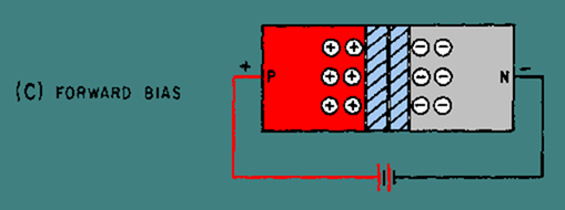
When a PN-junction diode is reverse biased, the majority carriers (holes in the P-material and electrons in the N-material) move away from the junction. The barrier or depletion region becomes wider, as illustrated in figure 3-1, (view A, view B, view C) and majority carrier current flow becomes very difficult across the high resistance of the wide depletion region. The presence of minority carriers causes a small leakage current that remains nearly constant for all reverse voltages up to a certain value. Once this value has been exceeded, there is a sudden increase in the reverse current. The voltage at which the sudden increase in current occurs is called the BREAKDOWN VOLTAGE. At breakdown, the reverse current increases very rapidly with a slight increase in the reverse voltage. Any diode can be reverse biased to the point of breakdown, but not every diode can safely dissipate the power associated with breakdown. A Zener diode is a PN junction designed to operate in the reverse-bias breakdown region.
Figure 3-1A. – Effects of bias on the depletion region of a PN junction. 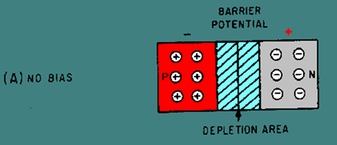
Figure 3-1B. – Effects of bias on the depletion region of a PN junction. 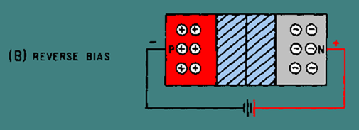
Figure 3-1C. – Effects of bias on the depletion region of a PN junction.
 There are two distinct theories used to explain the behavior of PN junctions during breakdown: one is the ZENER EFFECT and the other is the AVALANCHE EFFECT.
The ZENER EFFECT was first proposed by Dr. Carl Zener in 1934. According to Dr. Zener’s theory, electrical breakdown in solid dielectrics occurs by a process called QUANTUM-MECHANICAL TUNNELING. The Zener effect accounts for the breakdown below 5 volts; whereas, above 5 volts the breakdown is caused by the avalanche effect. Although the avalanche effect is now accepted as an explanation of diode breakdown, the term Zener diode is used to cover both types.
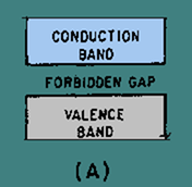
The true Zener effect in semiconductors can be described in terms of energy bands; however, only the two upper energy bands are of interest. The two upper bands, illustrated in figure 3-2, view A, are called the conduction band and the valence band.
Figure 3-2A. – Energy diagram for Zener diode.
The CONDUCTION BAND is a band in which the energy level of the electrons is high enough that the electrons will move easily under the influence of an external field. Since current flow is the movement of electrons, the readily mobile electrons in the conduction band are capable of maintaining a current flow when an external field in the form of a voltage is applied. Therefore, solid materials that have many electrons in the conduction band are called conductors.
The VALENCE BAND is a band in which the energy level is the same as the valence electrons of the atoms. Since the electrons in these levels are attached to the atoms, the electrons are not free to move around as are the conduction band electrons. With the proper amount of energy added, however, the electrons in the valence band may be elevated to the conduction band energy level. To do this, the electrons must cross a gap that exists between the valence band energy level and the conduction band energy level. This gap is known as the FORBIDDEN ENERGY BAND or FORBIDDEN GAP. The energy difference across this gap determines whether a solid material will act as a conductor, a semiconductor, or an insulator.
A conductor is a material in which the forbidden gap is so narrow that it can be considered nonexistent. A semiconductor is a solid that contains a forbidden gap, as shown in figure 3-2, view A. Normally, a semiconductor has no electrons at the conduction band energy level. The energy provided by room temperature heat, however, is enough energy to overcome the binding force of a few valence electrons and to elevate them to the conduction band energy level. The addition of impurities to the semiconductor material increases both the number of free electrons in the conduction band and the number of electrons in the valence band that can be elevated to the conduction band. Insulators are materials in which the forbidden gap is so large that practically no electrons can be given enough energy to cross the gap. Therefore, unless extremely large amounts of heat energy are available, these materials will not conduct electricity.
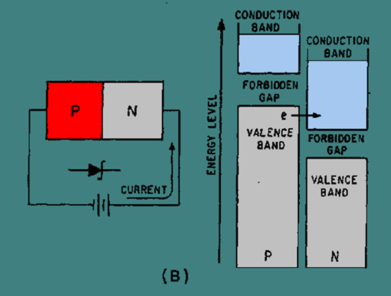
View B of figure 3-2 is an energy diagram of a reverse-biased Zener diode. The energy bands of the P and N materials are naturally at different levels, but reverse bias causes the valence band of the P material to overlap the energy level of the conduction band in the N material. Under this condition, the valence electrons of the P material can cross the extremely thin junction region at the overlap point without acquiring any additional energy. This action is called tunneling. When the breakdown point of the PN junction is reached, large numbers of minority carriers "tunnel" across the junction to form the current that occurs at breakdown. The tunneling phenomenon only takes place in heavily doped diodes such as Zener diodes.
Figure 3-2B. – Energy diagram for Zener diode.
The second theory of reverse breakdown effect in diodes is known as AVALANCHE breakdown and occurs at reverse voltages beyond 5 volts. This type of breakdown diode has a depletion region that is deliberately made narrower than the depletion region in the normal PN-junction diode, but thicker than that in the Zener-effect diode. The thicker depletion region is achieved by decreasing the doping level from the level used in Zener-effect diodes. The breakdown is at a higher voltage because of the higher resistivity of the material. Controlling the doping level of the material during the manufacturing process can produce breakdown voltages ranging between about 2 and 200 volts.
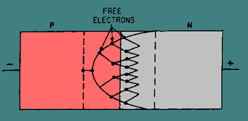
The mechanism of avalanche breakdown is different from that of the Zener effect. In the depletion region of a PN junction, thermal energy is responsible for the formation of electron-hole pairs. The leakage current is caused by the movement of minority electrons, which is accelerated in the electric field across the barrier region. As the reverse voltage across the depletion region is increased, the reverse voltage eventually reaches a critical value. Once the critical or breakdown voltage has been reached, sufficient energy is gained by the thermally released minority electrons to enable the electrons to rupture covalent bonds as they collide with lattice atoms. The released electrons are also accelerated by the electric field, resulting in the release of further electrons, and so on, in a chain or avalanche effect. This process is illustrated in figure 3-3.
Figure 3-3. – Avalanche multiplication.
For reverse voltage slightly higher than breakdown, the avalanche effect releases an almost unlimited number of carriers so that the diode essentially becomes a short circuit. The current flow in this region is limited only by an external series current-limiting resistor. Operating a diode in the breakdown region does not damage it, as long as the maximum power dissipation rating of the diode is not exceeded. Removing the reverse voltage permits all carriers to return to their normal energy values and velocities.
Some of the symbols used to represent Zener diodes are illustrated in figure 3-4 (view A, view B, view C, view D, and view E). Note that the polarity markings indicate electron flow is with the arrow symbol instead of against it as in a normal PN-junction diode. This is because breakdown diodes are operated in the reverse-bias mode, which means the current flow is by minority current carriers.
Figure 3-4A. – Schematic symbols for Zener diodes.
 Figure 3-4B. – Schematic symbols for Zener diodes.

Figure 3-4C. – Schematic symbols for Zener diodes.
Figure 3-4D. – Schematic symbols for Zener diodes. 
Figure 3-4E. – Schematic symbols for Zener diodes.

Zener diodes of various sorts are used for many purposes, but their most widespread use is as voltage regulators. Once the breakdown voltage of a Zener diode is reached, the voltage across the diode remains almost constant regardless of the supply voltage. Therefore they hold the voltage across the load at a constant level. This characteristic makes Zener diodes ideal voltage regulators, and they are found in almost all solid-state circuits in this capacity.
Q.1 In a reverse biased PN-junction, which current carriers cause leakage current?
Q.2 The action of a PN-junction during breakdown can be explained by what two theories?
Q.3 Which breakdown theory explains the action that takes place in a heavily doped PN-junction with a reverse bias of less than 5 volts?
Q.4 What is the doping level of an avalanche effect diode when compared to the doping level of a Zener-effect diode?
Q.5 During avalanche effect breakdown, what limits current flow through the diode?
Q.6 Why is electron flow with the arrow in the symbol of a Zener diode instead of against the arrow as it is in a normal diode?
Back
Home
Up
Next
The Tunnel Diode
In 1958, Leo Esaki, a Japanese scientist, discovered that if a semiconductor junction diode is heavily doped with impurities, it will have a region of negative resistance. The normal junction diode uses semiconductor materials that are lightly doped with one impurity atom for ten-million semiconductor atoms. This low doping level results in a relatively wide depletion region. Conduction occurs in the normal junction diode only if the voltage applied to it is large enough to overcome the potential barrier of the junction.
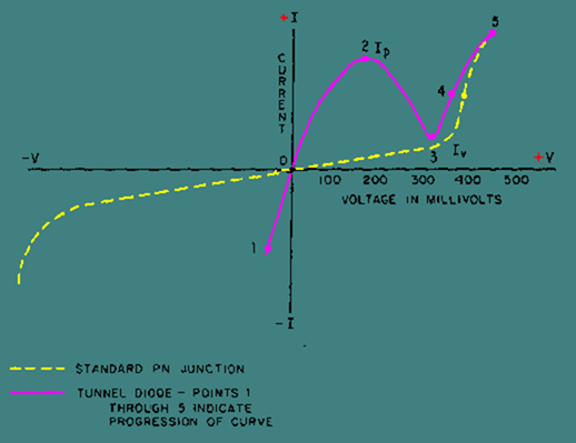
In the TUNNEL DIODE, the semiconductor materials used in forming a junction are doped to the extent of one-thousand impurity atoms for ten-million semiconductor atoms. This heavy doping produces an extremely narrow depletion zone similar to that in the Zener diode. Also because of the heavy doping, a tunnel diode exhibits an unusual current-voltage characteristic curve as compared with that of an ordinary junction diode. The characteristic curve for a tunnel diode is illustrated in figure 3-5.
Figure 3-5. – Characteristic curve of a tunnel diode compared to that of a standard PN junction.
The three most important aspects of this characteristic curve are (1) the forward current increase to a peak (IP) with a small applied forward bias, (2) the decreasing forward current with an increasing forward bias to a minimum valley current (IV), and (3) the normal increasing forward current with further increases in the bias voltage. The portion of the characteristic curve between IP and IV is the region of negative resistance. An explanation of why a tunnel diode has a region of negative resistance is best understood by using energy levels as in the previous explanation of the Zener effect.
Simply stated the theory known as quantum-mechanical tunneling is an electron crossing a PN-junction without having sufficient energy to do so otherwise. Because of the heavy doping the width of the depletion region is only one-millionth of an inch. You might think of the process simply as an arc-over between the N- and the P-side across the depletion region.
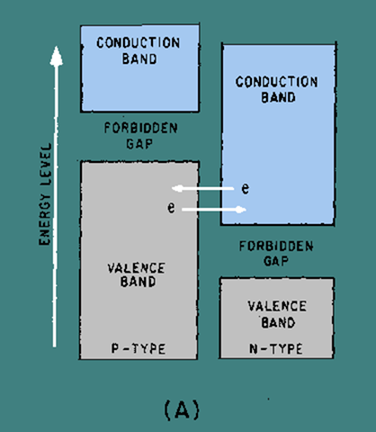
Figure 3-6 shows the equilibrium energy level diagram of a tunnel diode with no bias applied. Note in view A that the valence band of the P-material overlaps the conduction band of the N-material. The majority electrons and holes are at the same energy level in the equilibrium state. If there is any movement of current carriers across the depletion region due to thermal energy, the net current flow will be zero because equal numbers of current carriers flow in opposite directions. The zero net current flow is marked by a "0" on the current-voltage curve illustrated in view B.
Figure 3-6A. – Tunnel diode energy diagram with no bias.
Figure 3-6B. – Tunnel diode energy diagram with no bias.
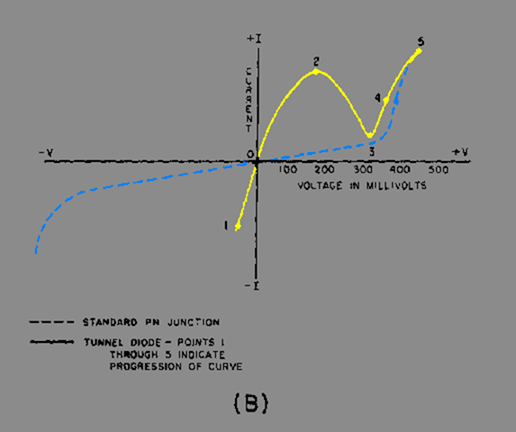
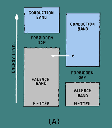
Figure 3-7, view A, shows the energy diagram of a tunnel diode with a small forward bias (50 millivolts) applied. The bias causes unequal energy levels between some of the majority carriers at the energy band overlap point, but not enough of a potential difference to cause the carriers to cross the forbidden gap in the normal manner. Since the valence band of the P-material and the conduction band of the N-material still overlap, current carriers tunnel across at the overlap and cause a substantial current flow. The amount of current flow is marked by point 2 on the curve in view B. Note in view A that the amount of overlap between the valence band and the conduction band decreased when forward bias was applied.
Figure 3-7A. – Tunnel diode energy diagram with 50 millivolts bias.
Figure 3-7B. – Tunnel diode energy diagram with 50 millivolts bias.
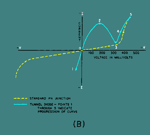
Figure 3-8, view A, is the energy diagram of a tunnel diode in which the forward bias has been increased to 450 millivolts. As you can see, the valence band and the conduction band no longer overlap at this point, and tunneling can no longer occur. The portion of the curve in view B from point 2 to point 3 shows the decreasing current that occurs as the bias is increased, and the area of overlap becomes smaller. As the overlap between the two energy bands becomes smaller, fewer and fewer electrons can tunnel across the junction. The portion of the curve between point 2 and point 3 in which current decreases as the voltage increases is the negative resistance region of the tunnel diode.
Figure 3-8A. – Tunnel diode energy diagram with 450 millivolts bias.

Figure 3-8B. – Tunnel diode energy diagram with 450 millivolts bias. 
Figure 3-9, view A, is the energy diagram of a tunnel diode in which the forward bias has been increased even further. The energy bands no longer overlap and the diode operates in the same manner as a normal PN junction, as shown by the portion of the curve in view (B) from point 3 to point 4.
Back
Home
Up
Next
Tunnel diode energy diagram
Figure 3-9A. – Tunnel diode energy diagram with 600 millivolts bias.
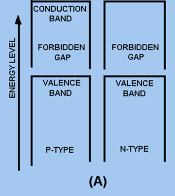
Figure 3-9B. – Tunnel diode energy diagram with 600 millivolts bias.
The negative resistance region is the most important and most widely used characteristic of the tunnel diode. A tunnel diode biased to operate in the negative resistance region can be used as either an oscillator or an amplifier in a wide range of frequencies and applications. Very high frequency applications using the tunnel diode are possible because the tunneling action occurs so rapidly that there is no transit time effect and therefore no signal distortion. Tunnel diodes are also used extensively in high-speed switching circuits because of the speed of the tunneling action.
Several schematic symbols are used to indicate a tunnel diode. These symbols are illustrated in figure 3-10 (view A, view B, view C, and view D).
Figure 3-10A. – Tunnel diode schematic symbols.
Figure 3-10B. – Tunnel diode schematic symbols.

Figure 3-10C. – Tunnel diode schematic symbols.

Figure 3-10D. – Tunnel diode schematic symbols.
Varactor
The VARACTOR, or varicap, as the schematic drawing in figure 3-11 suggests, is a diode that behaves like a variable capacitor, with the PN junction functioning like the dielectric and plates of a common capacitor. Understanding how the varactor operates is an important prerequisite to understanding field-effect transistors, which will be covered later in this topic.
Figure 3-11. – Varactor diode.

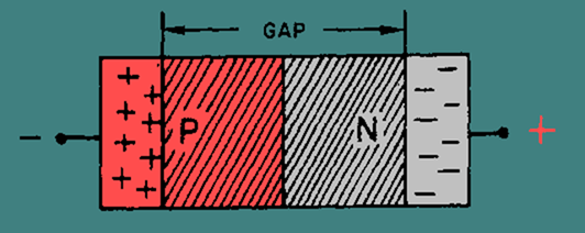
Figure 3-12 shows a PN junction. Surrounding the junction of the P and N materials is a narrow region void of both positively and negatively charged current carriers. This area is called the depletion region.
Figure 3-12. – PN junction. 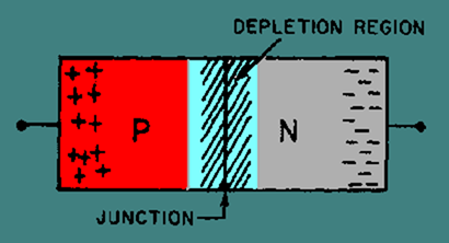
The size of the depletion region in a varactor diode is directly related to the bias. Forward biasing makes the region smaller by repelling the current carriers toward the PN junction. If the applied voltage is large enough (about .5 volt for silicon material), the negative particles will cross the junction and join with the positive particles, as shown in figure 3-13. This forward biasing causes the depletion region to decrease, producing a low resistance at the PN junction and a large current flow across it. This is the condition for a forward-biased diode. On the other hand, if reverse-bias voltage is applied to the PN junction, the size of its depletion region increases as the charged particles on both sides move away from the junction. This condition, shown in figure 3-14, produces a high resistance between the terminals and allows little current flow (only in the microampere range). This is the operating condition for the varactor diode, which is nothing more than a special PN junction.
Figure 3-13. – Forward-biased PN junction.
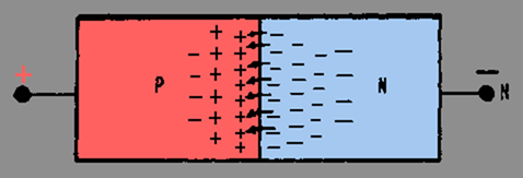
Figure 3-14. – Reverse-biased PN junction.
As the figure shows, the insulation gap formed by reverse biasing of the varactor is comparable to the layer of dielectric material between the plates of a common capacitor. Furthermore, the formula used to calculate capacitance
K = a constant value
d = distance between plates
can be applied to both the varactor and the capacitor. In this case, the size of the insulation gap of the varactor, or depletion region, is substituted for the distance between the plates of the capacitor. By varying the reverse-bias voltage applied to the varactor, the width of the "gap" may be varied. An increase in reverse bias increases the width of the gap (d) which reduces the capacitance (C) of the PN junction. Therefore, the capacitance of the varactor is inversely proportional to the applied reverse bias.
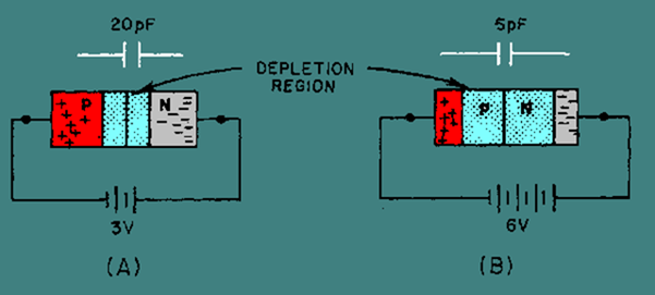
The ratio of varactor capacitance to reverse-bias voltage change may be as high as 10 to 1. Figure 3-15 shows one example of the voltage-to-capacitance ratio. View A shows that a reverse bias of 3 volts produces a capacitance of 20 picofarads in the varactor. If the reverse bias is increased to 6 volts, as shown in view B, the depletion region widens and capacitance drops to 5 picofarads. Each 1-volt increase in bias voltage causes a 5-picofarad decrease in the capacitance of the varactor; the ratio of change is therefore 5 to 1. Of course any decrease in applied bias voltage would cause a proportionate increase in capacitance, as the depletion region narrows. Notice that the value of the capacitance is small in the picofarad range.
Figure 3-15. – Varactor capacitance versus bias voltage.
In general, varactors are used to replace the old style variable capacitor tuning. They are used in tuning circuits of more sophisticated communication equipment and in other circuits where variable capacitance is required. One advantage of the varactor is that it allows a dc voltage to be used to tune a circuit for simple remote control or automatic tuning functions. One such application of the varactor is as a variable tuning capacitor in a receiver or transmitter tank circuit like that shown in figure 3-16.
Figure 3-16. – Varactor tuned resonant circuit.
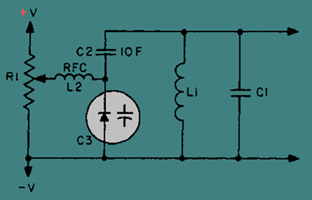
Figure 3-16 shows a dc voltage felt at the wiper of potentiometer R1 which can be adjusted between +V and -V. The dc voltage, passed through the low resistance of radio frequency choke L2, acts to reverse bias varactor diode C3. The capacitance of C3 is in series with C2, and the equivalent capacitance of C2 and C3 is in parallel with tank circuit L1-C1. Therefore, any variation in the dc voltage at R1 will vary both the capacitance of C3 and the resonant frequency of the tank circuit. The radio-frequency choke provides high inductive reactance at the tank frequency to prevent tank loading by R1. C2 acts to block dc from the tank as well as to fix the tuning range of C3.
An ohmmeter can be used to check a varactor diode in a circuit. A high reverse-bias resistance and a low forward-bias resistance with a 10 to 1 ratio in reverse-bias to forward-bias resistance is considered normal.
Q.7 What is the main difference in construction between normal PN junction diodes and tunnel diodes?
Q.8 What resistance property is found in tunnel diodes but not in normal diodes?
Q.9 When compared to the ordinary diode, the tunnel diode has what type of depletion region?
Q.10 In the tunnel diode, the tunneling current is at what level when the forbidden gap of the N-type material is at the same energy level as the empty states of the P-type material?
Q.11 The varactor displays what useful electrical property?
Q.12 When a PN junction is forward biased, what happens to the depletion region?
Q.13 When the reverse bias on a varactor is increased, what happens to the effective capacitance?
Back
Home
Up
Next

