Integrated Circuits: Introduction,High-Speed Design Techniques ,Optimization of Gate Level Design , Clocks and Clock,Schemes in High-Speed Circuit Design , Asynchronous Circuits and Systems , Interconnect Parasitics and Their Impact on High-Speed Design

Integrated Circuits

Introduction

Transistors and their fabrication into very large scale integrated (VLSI) circuits are the invention that has made modern computing possible. Since its inception, integrated circuits have been advancing rapidly from a few transistors on a small silicon die in the early 1960s to 4 millions of transistors integrated on to a single large silicon substrate. The dominant type of transistor used in today’s integrated circuits is the metal-oxide-semiconductor (MOS) type transistor. The rapid technological advances in integrated circuit (IC) technology accelerated during and after the 1980s, and one of the most influential factors for such a rapid advance is the technology scaling, that is, the reduction in MOS transistor feature sizes. The MOS feature size is typically measured by the MOS transistor channel length. The smaller the transistors, the more dense the integrated circuits in terms of the number of transistors packed on to a unit area of silicon substrate, and the faster the transistor can switch. Not only can we pack more transistors onto a unit silicon area, the chip size has also increase. As the transistor gets smaller and silicon chip size gets bigger, the transistor’s driving capability decreases and the interconnect parasitics (interconnect capacitance and resistance) increases. Consequently, the entire VLSI system has to be designed very carefully to meet the speed demands of the future. Common design issues include optimal gate design and transistor sizing, minimization of clock skew and proper timing budgeting, and realistic modeling of interconnect parasitics.

High-Speed Design Techniques

A modern VLSI device typically consists of several megacells, such as memory blocks and data-path arithmetic blocks, and a lot of basic MOS logic gates, such as inverters and NAND/NOR gates. Comple- mentary MOS (CMOS) is one of the most widely used logic families, mainly because of its low-power consumption and high-noise margin. Other logic families include NMOS and PMOS logic. Because of its popularity, only the CMOS logic will be discussed. Many approaches to high-speed design discussed here are equally applicable to other logic families.

Optimizing a VLSI device for high-speed operation can be carried out at the system level, as well as at the circuit and logic level. To achieve the maximum operating speed at the circuit and logic levels for a given technology, it is essential to properly set the size of each transistor in a logic gate to optimally drive the output load. If the output load is very large, a string of drivers with geometrically increasing sizes is needed. The size of transistors in a logic gate is also determined by the impact of the transistors as a load to be driven by their preceding gates.

Optimization of Gate Level Design

To optimize the gate level design, let us look at the performance of a single CMOS inverter as shown in Fig. 5.1. Delay of a gate is typically defined as the time difference between input transition and output transition at 50% of supply voltage. The inverter gate delay can be analytically expressed as

image

where Cl is the load capacitance of the inverter; βn and βp are the forward current gains of n-type and p-type transistors, respectively, and are proportional to the transistor’s channel width and inversely proportional to the transistor’s channel length; An and Ap are process related parameters for a given supply voltage and they are determined by

image

where n = Vthn / Vdd and p = Vth p / Vdd . Vthn and Vth p are gate threshold voltages for n-channel and p-channel transistors, respectively. This expression does not take the input signal slope into account. Otherwise, the expression would become more complicated. For more complex CMOS gates, an equivalent inverter structure is constructed to reflect the effective strength of their p-tree and n-tree in order to apply the inverter delay model.

In practice, CMOS gate delay is treated in a simple fashion. The delay of a logic gate can be divided into two parts: the intrinsic delay Dins, and the load-related delay Dload. The gate intrinsic delay is determined by the internal characteristics of the gate including the implementing technology, the gate structure, and the transistor sizes. The load-related delay is a function of the total load capacitance at the gate’s output. The total gate delay can be expressed as

imagewhere Cl is the total load capacitance and S is the factor for gate’s driving strength. C S represents the gate’s load-related delay. In most CMOS circuits using leading-edge submicron technologies, the total delay of a gate can be dominated by the load-related delay. For an inverter in a modern submicron CMOS technology of around 0.5-µm feature size, Dins can range from 0.08 to 0.12 ns and S can range from 0.00065 to 0.00085 ns/fF depending on specifics in the technology and the minimum transistor feature size. For other more complex gates such as NAND and NOR gates, Dins and S generally increase.

To optimize a VLSI circuit for its maximum operating speed, critical paths must be identified. A critical path in a circuit is a signal path with the longest time delay from a primary input to a primary output. The time delay on the critical path in a circuit determines the maximum operating speed of the circuit. The time delay of a critical path can be minimized by altering the size of the transistors on the critical path. Using the lumped resistor-capacitor (RC) delay model, the problem of transistor sizing can be formulated to an optimization problem with a convex relationship between the path delay and the sizes of the transistors on the path. This optimization problem is simple to solve. The solutions often have 20–30% deviation, however, compared to the SPICE simulation results. Realistic modeling of gate delay taking some second- order variables, such as input signal slope, into consideration has shown that the relationship between the path delay and the sizes of the transistors on the path is not convex. Such detailed analysis led to more sophisticated transistor sizing algorithms. One of these algorithms suggested using genetic methods to search for an optimal solution and has shown some promising results.

Clocks and Clock Schemes in High-Speed Circuit Design

Most of the modern electronic systems are synchronous systems. The clock is a central pace setter in a synchronous system to step the desired system operations through various stages of the computation.
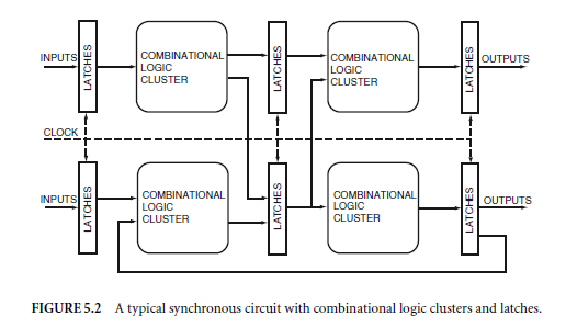
imageLatches are often used to facilitate catching the output data at the end of each clock cycle. Figure 5.2 shows the typical synchronous circuit with random logic clusters as computational blocks and latches as pace setting devices. When there exist feedbacks, as shown in Fig. 5.2, the circuit is referred to as sequential circuit. A latch is also called a register or a flip-flop. The way a latch catches data depends on how it is triggered by the clock signal. Generally, there are level-triggered and edge-triggered latches, the former can be further subdivided according to the triggering polarity as positive or negative level or edge-triggered latches. The performance of a digital circuit is often determined by the maximum clock frequency the circuit can run. For a synchronous digital circuit to function properly, the longest delay through any combinational clusters must be less than the clock cycle period. Therefore, the following needs to be done for high-speed design:

  • Partition the entire system so that the delays of all of the combinational clusters are as balanced as possible.
  • Design the circuit of the combinational clusters so that the delay of critical paths in the circuit is

minimized and less than the desired clock cycle period.

  • Use a robust clock scheme to ensure that the entire system is free of race conditions and has minimal tolerable clock skew.

The first item listed is beyond the scope of this section. The second item was discussed in the preceding subsection.

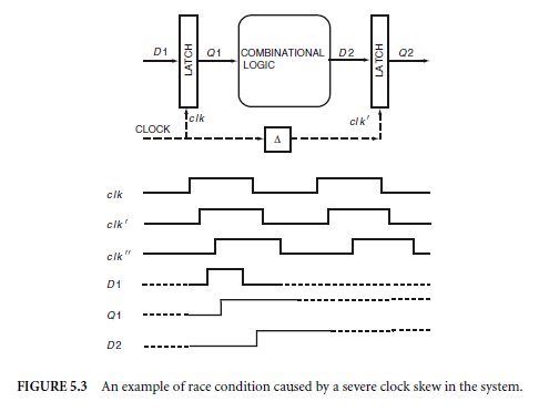
Race conditions typically occur with the use of level triggered latches. Figure 5.3 shows a typical syn- chronous system based on level triggered latches. Because of delays on the clock distribution network, such as buffers and capacitive parasitics on the interconnect, the timing difference caused by such a distribution delay is often referred to as clock skew which is modeled by a delay element in Fig. 5.3. For the system to operate properly, at the positive edge each latch is supposed to capture its input data from the previous

clock cycle. If the clock skew is severe shown as skewed clock cl k∓∓, however, it could be possible that the delay from Q1 to D2 becomes short enough that D1 is not only caught by the cl k, but also caught by cl k∓.

The solution to such a race condition caused by severe clock skew is as follows:

  • Change the latch elements from level triggered to edge triggered or pseudoedge triggered latches such as latches using two-phase, nonoverlapping clocks.
  • Resynthesize the system to balance to the critical path delay of different combinational clusters.
  • Reduce the clock skew.

Clock skew can also cause other types of circuit malfunction if it is not attended properly. In dynamic logic, severe clock skew may result in different functional blocks being in different stages of precharging
imageor evaluating. Severe clock skew eats away a significant amount of precious cycle time in VLSI systems. Therefore, reducing clock skew is an important problem in high-speed circuit design.

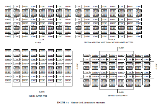
As discussed earlier, clock skew is mainly caused by the imbalance of the clock distribution network. Such an imbalance can be the result of distance differences from the nearest clock driver, different functional blocks driven by different clock drivers with different driving strengths, temperature difference on the same die, device characteristic differences on the same die due to process variation, etc. Two general approaches are often taken to minimize the clock skew. The first approach deals with the way the clock signal is distributed. The geometric shape of the clock distribution network is a very important attribute. Depending on the type of system operation, several popular distribution network topologies are illustrated in Fig. 5.4. Among these topologies, H-tree presents least amount of clock skew and, therefore, is widely used in high-performance systems.

clip_image020clip_image020[1]The second approach deals with employing additional on-chip circuits to force the clock signals of two different functional blocks to be aligned, or to force the on-chip clock signal to be aligned with the global clock signal at the system level. The widely used circuits for this purpose include phase-locked loop (PLL) and delay-locked loop (DLL). Figure 5.5 shows a simple phase-locked loop. A simple PLL consists of four components: a digital phase detector, a charge pump, a low-pass filter, and a voltage controlled oscillator (VCO). The phase detector accepts reference clock, CLK ref, and a skewed clock, CLK out, and compares the phase difference of the two clocks to charge or discharge the charge pump. The low-pass filter is used to convert the phase difference between the reference frequency and the skewed frequency to a voltage level. This voltage is then fed into the VCO to reduce the difference of the reference and skewed clocks until they are locked to each other.

One of the most important design parameters for PLL is the output jitter. The output jitter is demonstrated by the random deviation of the output clock’s phase from the reference clock signal. Significant peak-to-peak jitter will effectively reduce the clock period. The main contributor of the output jitter is the noise on the input of the VCO. Additional jitter can be induced by the noise on power supply rails that are common to high-speed VLSI circuits. Furthermore, acquisition time of PLL, in the several microsecond range, is often longer than desirable. This is mainly attributed to the response time of the VCO. In a typical scenario where clock skew is caused by the imbalance of the distribution network, the skewed clock often has the correct frequency. What needs to be corrected is the relative phase of the clock signals. Therefore, there is no need to have a VCO. Rather, a simple delay logic can be used to modify the clock signal’s phase.

image

image

This type of simplified phase correct circuit is referred to as a delay-locked loop. By replacing the VCO with a simple programmable delay line, DLL is simpler, yet exhibits less jitter than its PLL counterpart.

Asynchronous Circuits and Systems

Clock distribution within large VLSI chips is becoming more and more of a problem for high-speed digital systems. Such a problem may be surmountable using state-of-the-art computer aided design (CAD) tools and on-chip PLL/DLL circuits. Asynchronous circuits have, nevertheless, gained a great deal of attention lately. An asynchronous circuit does not require an external clock to get it through the computation. Instead, it works on the principle of handshaking between functional blocks. Therefore, execution of a computational operation is totally dependent on the readiness of all of the input variables of the functional block. The biggest advantage of asynchronous circuits over synchronous circuits is that the correct behavior of asynchronous circuits is independent of the speed of their components or signal interconnect delays.

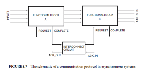
In a typical asynchronous circuit, functional blocks will have two more signals, request and complete, apart from their input and output signals as shown in Fig. 5.6. These two binary signals are necessary and sufficient for handshaking purposes. Even though asynchronous circuits are speed independent, the order of computation is still maintained by connecting the complete signal from one block to the request signal to another block. When the request signal is active for a functional block, indicating the computation of the preceding functional block is completed, the current functional block starts computation evaluation using its valid inputs from the preceding functional block. Once the evaluation is completed, the current functional block sets the complete signal to active to activate other functional blocks for computation. Figure 5.7 shows a schematic of such a communication protocol where block A and block B are connected in a pipeline.

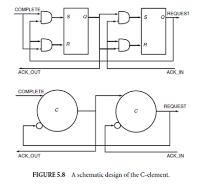
To ensure that asynchronous circuits function correctly regardless of individual block speed, the request signal of a functional block should only be activated if the functional block has already completed the cur- rent computation. Otherwise, the current computation would be overwritten by incoming computation requests. To prevent this situation from happening, an interconnection block is required with an acknowl- edge signal from the current functional block to the preceding functional block. An active acknowledge signal indicates to the preceding function block that the current block is ready to accept new data from it. This two-way communication protocol with request and acknowledge is illustrated in Fig. 5.7. The interconnect circuit is unique to asynchronous circuits. It is often referred to as a C-element. Figure 5.8 shows a design of the C-element.

In recent years, much effort has been spent on applying the asynchronous circuits to real-world ap- plications. Several totally asynchronous designs of microprocessors have demonstrated their commercial feasibility. Several issues that still need to be addressed with regard to asynchronous circuits include

image

image

acceptable amounts of silicon overhead, power efficiency, and performance as compared to their synchronous counterparts.

Interconnect Parasitics and Their Impact on High-Speed Design

On-chip interconnects present parasitic capacitance and resistance as loads to active circuits. Such parasitic loads had little impact on earlier ICs because the intrinsic gate delay dominated the total gate delay. With aggressive scaling in the VLSI process, the gate intrinsic delay decreases dramatically. The interconnect parasitics does not scale proportionally, however, and the wire resistance tends to increase, resulting in the delay caused by the interconnect load parasitics gradually becoming a dominant factor in the total gate delay. The problem is further exacerbated by the fact that when the operating speed reaches several hundred megahertz, the traditional lumped RC model is no longer accurate. It has been suggested that such a lumped RC model should be modified to include a grounded resistor and an inductor. The RLC interconnect model includes nonequilibrium initial conditions and its response waveform may be nonmonotonic. Such a model may be more accurate because the existence of the inductance reduces the rate of increase in current and, therefore, increases the signal transition time. When the operating speed increases further such that the rise time of a signal is much less than the signal transmission time from point A to point B, a transmission line model should be used. On-chip interconnect, thus, is typically modeled as a microstrip.
image


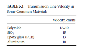
imageThe characteristics of a transmission line are determined by its relative dielectric constant and magnetic permeability. Table 5.1 shows the signal transmission velocity in some common materials used in VLSI.

As a rule of thumb, the transmission line phenomena become significant when

image

where tr is the rise time of a signal and t f is the signal transmission time, which is the interconnect length divided by the signal traveling velocity in the given material. The interconnect can be treated as a lumped RC network when

tr > 5∗t f

The signal rise time depends on the driver design and the transmission line’s characteristic impedance Z0. In MOS ICs, the load device at the receiving end of the transmission line can always be treated as an open circuit. Therefore, driver design is a very important aspect of high-speed circuit design. The ideal case is to have the driver’s output impedance match the transmission line’s characteristic impedance. Driving an unterminated transmission line (the MOS IC case) with its output impedance lower than the line’s characteristic impedance, however, can increase driver’s settling time due to excess ringing and, therefore, is definitely to be avoided. Excess ringing at the receiving end could also cause the load to switch undesirably. Assuming MOS transistor’s threshold is 0.6–0.8 V, to ensure that no undesirable switching takes place, the output impedance of the drive should be at least a third of the charactertstic impedance of the transmission line. When the output impedance is higher than the line’s characteristic impedance, multiple wave trips of the signal may be required to switch the load. To ensure that only one wave trip is needed to switch the load, the output impedance of the driver should be within 60% of the characteristic impedance of the transmission line.

For a lossy transmission line due to parasitic resistance of on-chip interconnects, an exponential attenuating transfer function can be applied to the signal transfer at any point on the transmission line. The rate of the attenuation is proportional to the unit resistance of the interconnect. When operating frequency increases beyond a certain level, the on-chip transmission media exhibits the skin effect in which the time-varying currents concentrate near the skin of the conductor. Therefore, the unit resistance of the transmission media increases dramatically.

Defining Terms

Application-specific integrated circuit (ASIC): Device designed specifically for a particular application.

Application-specific standard product (ASSP): Device designed specifically for one area of applications,

such as graphics and video processing.

Asynchronous system: A system in which the progress of a computation is driven by the readiness of all the necessary input variables for the computation through a handshaking protocol. Therefore, no central clock is needed.

C-element: A circuit used in an asynchronous as an interconnect circuit. The function of this circuit is to facilitate the handshaking communication protocol between two functional blocks.

Clock skew: A phase difference between two clock signals at different part of a chip/system due to imbalance of the distribution media and the distribution network.

Complementary metal-oxide silicon (CMOS): It is a very popular integrated circuit type in use today.

Critical path: A signal path from a primary input pin to a primary output pin with the longest delay timein a logic block.

Delay-locked loop (DLL): It is similar to PLL except that it has better jitter suppression capability.

Digital signal processor (DSP): A processing device specialized in popular math routines used by signal processing algorithms.

Field programmable gate array (FPGA): A popular device which can be tailored to a particular application by loading a customizing program on to the chip.

H-tree: A popular clock distribution tree topologically that resembles the H shape. It introduces the leastamount of clock skew compared to other distribution topologies.

Phase-locked loop (PLL): A circuit that can detect the phase difference of two signals and reduce the difference in the presence of the phase difference.

Programmable logic devices (PLD): A class of IC products which are easy to customize for a particular application.

SPICE: A popular circuit level simulation program to perform detailed analysis of circuit behavior.

Synchronous system: A system in which a computation is divided into unit periods defined by a central clock signal. Signal transfer within the system typically occurred at the transition edge of the clock signal.

References

Bakoglu, H.B. 1991. Circuits, Interconnections, and Packaging for VLSI. Addison-Wesley, Reading, MA.

Dill, D.L. 1989. Trace Theory for Automatic Hierarchical Verification of Speed-Independent Circuits. MIT Press, Cambridge, MA.

Gardner, F.M. 1979. Phaselock Techniques, 2nd ed. Wiley, New York.

Jeong, D. et al. 1987. Design of PLL-based clock generation circuits. IEEE J. Solid-State Circuits SC-22(2):

255–261.

Johnson, M. and Hudson, E. 1988. A variable delay line PLL for CPU-coprocessor synchronization. IEEE

J. Solid-State Circuits (Oct.):1218–1223.

Meng, T.H. 1991. Synchronization Design for Digital Systems. Kluwer Academic, Norwell, MA.

Rosenstark, S. 1994. Transmission Lines in Computer Engineering. McGraw-Hill, New York.

Sapatnekar, S., Rao, V., and Vaidya, P. 1992. A convex optimization approach to transistor sizing for CMOS

circuits. Proc. ICCAD, pp. 482–485.

Wang, X. and Chen, T. 1995. Performance and area optimization of VLSI systems using genetic algorithms.

Int. J. of VLSI Design 3(1):43–51.

Weste, N. and Eshraghian, K. 1993. Principle of CMOS VLSI Design: A Systems Perspective, 2nd ed. Addison-

Wesley, Reading, MA.

Further Information

For general information on the VLSI design process and various design issues, consult several excellent reference books, two of which are listed in the reference section, including Mead and Conway’s Introduction to VLSI Systems, Glasser and Dobberpuhl’s The Design and Analysis of VLSI Circuits, and Geiger’s VLSI Design Techniques for Analog and Digital Circuits. IEEE Journal of Solid-State Circuits provides an excellent source for the latest development of novel and high-performance VLSI devices.

Some of the latest applications of PLLs and DLLs can be found in the Proceedings of International Solid- State Circuit Conference, the Symposium on VLSI Circuits, and the Custom Integrated Circuit Conference.

For information on modeling of VLSI interconnects and their transmission line treatment, consult the Proceedings of Design Automation Conference and International Conference on Computer-Aided Design. IEEE Transactions on CAD is also an excellent source of information on the subject.

Leave a comment

Your email address will not be published. Required fields are marked *

Integrated Circuits: Introduction,High-Speed Design Techniques ,Optimization of Gate Level Design , Clocks and Clock,Schemes in High-Speed Circuit Design , Asynchronous Circuits and Systems , Interconnect Parasitics and Their Impact on High-Speed Design

Integrated Circuits

Introduction

Transistors and their fabrication into very large scale integrated (VLSI) circuits are the invention that has made modern computing possible. Since its inception, integrated circuits have been advancing rapidly from a few transistors on a small silicon die in the early 1960s to 4 millions of transistors integrated on to a single large silicon substrate. The dominant type of transistor used in today’s integrated circuits is the metal-oxide-semiconductor (MOS) type transistor. The rapid technological advances in integrated circuit (IC) technology accelerated during and after the 1980s, and one of the most influential factors for such a rapid advance is the technology scaling, that is, the reduction in MOS transistor feature sizes. The MOS feature size is typically measured by the MOS transistor channel length. The smaller the transistors, the more dense the integrated circuits in terms of the number of transistors packed on to a unit area of silicon substrate, and the faster the transistor can switch. Not only can we pack more transistors onto a unit silicon area, the chip size has also increase. As the transistor gets smaller and silicon chip size gets bigger, the transistor’s driving capability decreases and the interconnect parasitics (interconnect capacitance and resistance) increases. Consequently, the entire VLSI system has to be designed very carefully to meet the speed demands of the future. Common design issues include optimal gate design and transistor sizing, minimization of clock skew and proper timing budgeting, and realistic modeling of interconnect parasitics.

High-Speed Design Techniques

A modern VLSI device typically consists of several megacells, such as memory blocks and data-path arithmetic blocks, and a lot of basic MOS logic gates, such as inverters and NAND/NOR gates. Comple- mentary MOS (CMOS) is one of the most widely used logic families, mainly because of its low-power consumption and high-noise margin. Other logic families include NMOS and PMOS logic. Because of its popularity, only the CMOS logic will be discussed. Many approaches to high-speed design discussed here are equally applicable to other logic families.

Optimizing a VLSI device for high-speed operation can be carried out at the system level, as well as at the circuit and logic level. To achieve the maximum operating speed at the circuit and logic levels for a given technology, it is essential to properly set the size of each transistor in a logic gate to optimally drive the output load. If the output load is very large, a string of drivers with geometrically increasing sizes is needed. The size of transistors in a logic gate is also determined by the impact of the transistors as a load to be driven by their preceding gates.

Optimization of Gate Level Design

To optimize the gate level design, let us look at the performance of a single CMOS inverter as shown in Fig. 5.1. Delay of a gate is typically defined as the time difference between input transition and output transition at 50% of supply voltage. The inverter gate delay can be analytically expressed as

image

where Cl is the load capacitance of the inverter; βn and βp are the forward current gains of n-type and p-type transistors, respectively, and are proportional to the transistor’s channel width and inversely proportional to the transistor’s channel length; An and Ap are process related parameters for a given supply voltage and they are determined by

image

where n = Vthn / Vdd and p = Vth p / Vdd . Vthn and Vth p are gate threshold voltages for n-channel and p-channel transistors, respectively. This expression does not take the input signal slope into account. Otherwise, the expression would become more complicated. For more complex CMOS gates, an equivalent inverter structure is constructed to reflect the effective strength of their p-tree and n-tree in order to apply the inverter delay model.

In practice, CMOS gate delay is treated in a simple fashion. The delay of a logic gate can be divided into two parts: the intrinsic delay Dins, and the load-related delay Dload. The gate intrinsic delay is determined by the internal characteristics of the gate including the implementing technology, the gate structure, and the transistor sizes. The load-related delay is a function of the total load capacitance at the gate’s output. The total gate delay can be expressed as

imagewhere Cl is the total load capacitance and S is the factor for gate’s driving strength. C S represents the gate’s load-related delay. In most CMOS circuits using leading-edge submicron technologies, the total delay of a gate can be dominated by the load-related delay. For an inverter in a modern submicron CMOS technology of around 0.5-µm feature size, Dins can range from 0.08 to 0.12 ns and S can range from 0.00065 to 0.00085 ns/fF depending on specifics in the technology and the minimum transistor feature size. For other more complex gates such as NAND and NOR gates, Dins and S generally increase.

To optimize a VLSI circuit for its maximum operating speed, critical paths must be identified. A critical path in a circuit is a signal path with the longest time delay from a primary input to a primary output. The time delay on the critical path in a circuit determines the maximum operating speed of the circuit. The time delay of a critical path can be minimized by altering the size of the transistors on the critical path. Using the lumped resistor-capacitor (RC) delay model, the problem of transistor sizing can be formulated to an optimization problem with a convex relationship between the path delay and the sizes of the transistors on the path. This optimization problem is simple to solve. The solutions often have 20–30% deviation, however, compared to the SPICE simulation results. Realistic modeling of gate delay taking some second- order variables, such as input signal slope, into consideration has shown that the relationship between the path delay and the sizes of the transistors on the path is not convex. Such detailed analysis led to more sophisticated transistor sizing algorithms. One of these algorithms suggested using genetic methods to search for an optimal solution and has shown some promising results.

Clocks and Clock Schemes in High-Speed Circuit Design

Most of the modern electronic systems are synchronous systems. The clock is a central pace setter in a synchronous system to step the desired system operations through various stages of the computation.

imageLatches are often used to facilitate catching the output data at the end of each clock cycle. Figure 5.2 shows the typical synchronous circuit with random logic clusters as computational blocks and latches as pace setting devices. When there exist feedbacks, as shown in Fig. 5.2, the circuit is referred to as sequential circuit. A latch is also called a register or a flip-flop. The way a latch catches data depends on how it is triggered by the clock signal. Generally, there are level-triggered and edge-triggered latches, the former can be further subdivided according to the triggering polarity as positive or negative level or edge-triggered latches. The performance of a digital circuit is often determined by the maximum clock frequency the circuit can run. For a synchronous digital circuit to function properly, the longest delay through any combinational clusters must be less than the clock cycle period. Therefore, the following needs to be done for high-speed design:

  • Partition the entire system so that the delays of all of the combinational clusters are as balanced as possible.
  • Design the circuit of the combinational clusters so that the delay of critical paths in the circuit is

minimized and less than the desired clock cycle period.

  • Use a robust clock scheme to ensure that the entire system is free of race conditions and has minimal tolerable clock skew.

The first item listed is beyond the scope of this section. The second item was discussed in the preceding subsection.

Race conditions typically occur with the use of level triggered latches. Figure 5.3 shows a typical syn- chronous system based on level triggered latches. Because of delays on the clock distribution network, such as buffers and capacitive parasitics on the interconnect, the timing difference caused by such a distribution delay is often referred to as clock skew which is modeled by a delay element in Fig. 5.3. For the system to operate properly, at the positive edge each latch is supposed to capture its input data from the previous

clock cycle. If the clock skew is severe shown as skewed clock cl k∓∓, however, it could be possible that the delay from Q1 to D2 becomes short enough that D1 is not only caught by the cl k, but also caught by cl k∓.

The solution to such a race condition caused by severe clock skew is as follows:

  • Change the latch elements from level triggered to edge triggered or pseudoedge triggered latches such as latches using two-phase, nonoverlapping clocks.
  • Resynthesize the system to balance to the critical path delay of different combinational clusters.
  • Reduce the clock skew.

Clock skew can also cause other types of circuit malfunction if it is not attended properly. In dynamic logic, severe clock skew may result in different functional blocks being in different stages of precharging

imageor evaluating. Severe clock skew eats away a significant amount of precious cycle time in VLSI systems. Therefore, reducing clock skew is an important problem in high-speed circuit design.

As discussed earlier, clock skew is mainly caused by the imbalance of the clock distribution network. Such an imbalance can be the result of distance differences from the nearest clock driver, different functional blocks driven by different clock drivers with different driving strengths, temperature difference on the same die, device characteristic differences on the same die due to process variation, etc. Two general approaches are often taken to minimize the clock skew. The first approach deals with the way the clock signal is distributed. The geometric shape of the clock distribution network is a very important attribute. Depending on the type of system operation, several popular distribution network topologies are illustrated in Fig. 5.4. Among these topologies, H-tree presents least amount of clock skew and, therefore, is widely used in high-performance systems.

clip_image020clip_image020[1]The second approach deals with employing additional on-chip circuits to force the clock signals of two different functional blocks to be aligned, or to force the on-chip clock signal to be aligned with the global clock signal at the system level. The widely used circuits for this purpose include phase-locked loop (PLL) and delay-locked loop (DLL). Figure 5.5 shows a simple phase-locked loop. A simple PLL consists of four components: a digital phase detector, a charge pump, a low-pass filter, and a voltage controlled oscillator (VCO). The phase detector accepts reference clock, CLK ref, and a skewed clock, CLK out, and compares the phase difference of the two clocks to charge or discharge the charge pump. The low-pass filter is used to convert the phase difference between the reference frequency and the skewed frequency to a voltage level. This voltage is then fed into the VCO to reduce the difference of the reference and skewed clocks until they are locked to each other.

One of the most important design parameters for PLL is the output jitter. The output jitter is demonstrated by the random deviation of the output clock’s phase from the reference clock signal. Significant peak-to-peak jitter will effectively reduce the clock period. The main contributor of the output jitter is the noise on the input of the VCO. Additional jitter can be induced by the noise on power supply rails that are common to high-speed VLSI circuits. Furthermore, acquisition time of PLL, in the several microsecond range, is often longer than desirable. This is mainly attributed to the response time of the VCO. In a typical scenario where clock skew is caused by the imbalance of the distribution network, the skewed clock often has the correct frequency. What needs to be corrected is the relative phase of the clock signals. Therefore, there is no need to have a VCO. Rather, a simple delay logic can be used to modify the clock signal’s phase.

image

image

This type of simplified phase correct circuit is referred to as a delay-locked loop. By replacing the VCO with a simple programmable delay line, DLL is simpler, yet exhibits less jitter than its PLL counterpart.

Asynchronous Circuits and Systems

Clock distribution within large VLSI chips is becoming more and more of a problem for high-speed digital systems. Such a problem may be surmountable using state-of-the-art computer aided design (CAD) tools and on-chip PLL/DLL circuits. Asynchronous circuits have, nevertheless, gained a great deal of attention lately. An asynchronous circuit does not require an external clock to get it through the computation. Instead, it works on the principle of handshaking between functional blocks. Therefore, execution of a computational operation is totally dependent on the readiness of all of the input variables of the functional block. The biggest advantage of asynchronous circuits over synchronous circuits is that the correct behavior of asynchronous circuits is independent of the speed of their components or signal interconnect delays.

In a typical asynchronous circuit, functional blocks will have two more signals, request and complete, apart from their input and output signals as shown in Fig. 5.6. These two binary signals are necessary and sufficient for handshaking purposes. Even though asynchronous circuits are speed independent, the order of computation is still maintained by connecting the complete signal from one block to the request signal to another block. When the request signal is active for a functional block, indicating the computation of the preceding functional block is completed, the current functional block starts computation evaluation using its valid inputs from the preceding functional block. Once the evaluation is completed, the current functional block sets the complete signal to active to activate other functional blocks for computation. Figure 5.7 shows a schematic of such a communication protocol where block A and block B are connected in a pipeline.

To ensure that asynchronous circuits function correctly regardless of individual block speed, the request signal of a functional block should only be activated if the functional block has already completed the cur- rent computation. Otherwise, the current computation would be overwritten by incoming computation requests. To prevent this situation from happening, an interconnection block is required with an acknowl- edge signal from the current functional block to the preceding functional block. An active acknowledge signal indicates to the preceding function block that the current block is ready to accept new data from it. This two-way communication protocol with request and acknowledge is illustrated in Fig. 5.7. The interconnect circuit is unique to asynchronous circuits. It is often referred to as a C-element. Figure 5.8 shows a design of the C-element.

In recent years, much effort has been spent on applying the asynchronous circuits to real-world ap- plications. Several totally asynchronous designs of microprocessors have demonstrated their commercial feasibility. Several issues that still need to be addressed with regard to asynchronous circuits include

image

image

acceptable amounts of silicon overhead, power efficiency, and performance as compared to their synchronous counterparts.

Interconnect Parasitics and Their Impact on High-Speed Design

On-chip interconnects present parasitic capacitance and resistance as loads to active circuits. Such parasitic loads had little impact on earlier ICs because the intrinsic gate delay dominated the total gate delay. With aggressive scaling in the VLSI process, the gate intrinsic delay decreases dramatically. The interconnect parasitics does not scale proportionally, however, and the wire resistance tends to increase, resulting in the delay caused by the interconnect load parasitics gradually becoming a dominant factor in the total gate delay. The problem is further exacerbated by the fact that when the operating speed reaches several hundred megahertz, the traditional lumped RC model is no longer accurate. It has been suggested that such a lumped RC model should be modified to include a grounded resistor and an inductor. The RLC interconnect model includes nonequilibrium initial conditions and its response waveform may be nonmonotonic. Such a model may be more accurate because the existence of the inductance reduces the rate of increase in current and, therefore, increases the signal transition time. When the operating speed increases further such that the rise time of a signal is much less than the signal transmission time from point A to point B, a transmission line model should be used. On-chip interconnect, thus, is typically modeled as a microstrip.

image


imageThe characteristics of a transmission line are determined by its relative dielectric constant and magnetic permeability. Table 5.1 shows the signal transmission velocity in some common materials used in VLSI.

As a rule of thumb, the transmission line phenomena become significant when

image

where tr is the rise time of a signal and t f is the signal transmission time, which is the interconnect length divided by the signal traveling velocity in the given material. The interconnect can be treated as a lumped RC network when

tr > 5∗t f

The signal rise time depends on the driver design and the transmission line’s characteristic impedance Z0. In MOS ICs, the load device at the receiving end of the transmission line can always be treated as an open circuit. Therefore, driver design is a very important aspect of high-speed circuit design. The ideal case is to have the driver’s output impedance match the transmission line’s characteristic impedance. Driving an unterminated transmission line (the MOS IC case) with its output impedance lower than the line’s characteristic impedance, however, can increase driver’s settling time due to excess ringing and, therefore, is definitely to be avoided. Excess ringing at the receiving end could also cause the load to switch undesirably. Assuming MOS transistor’s threshold is 0.6–0.8 V, to ensure that no undesirable switching takes place, the output impedance of the drive should be at least a third of the charactertstic impedance of the transmission line. When the output impedance is higher than the line’s characteristic impedance, multiple wave trips of the signal may be required to switch the load. To ensure that only one wave trip is needed to switch the load, the output impedance of the driver should be within 60% of the characteristic impedance of the transmission line.

For a lossy transmission line due to parasitic resistance of on-chip interconnects, an exponential attenuating transfer function can be applied to the signal transfer at any point on the transmission line. The rate of the attenuation is proportional to the unit resistance of the interconnect. When operating frequency increases beyond a certain level, the on-chip transmission media exhibits the skin effect in which the time-varying currents concentrate near the skin of the conductor. Therefore, the unit resistance of the transmission media increases dramatically.

Defining Terms

Application-specific integrated circuit (ASIC): Device designed specifically for a particular application.

Application-specific standard product (ASSP): Device designed specifically for one area of applications,

such as graphics and video processing.

Asynchronous system: A system in which the progress of a computation is driven by the readiness of all the necessary input variables for the computation through a handshaking protocol. Therefore, no central clock is needed.

C-element: A circuit used in an asynchronous as an interconnect circuit. The function of this circuit is to facilitate the handshaking communication protocol between two functional blocks.

Clock skew: A phase difference between two clock signals at different part of a chip/system due to imbalance of the distribution media and the distribution network.

Complementary metal-oxide silicon (CMOS): It is a very popular integrated circuit type in use today.

Critical path: A signal path from a primary input pin to a primary output pin with the longest delay timein a logic block.

Delay-locked loop (DLL): It is similar to PLL except that it has better jitter suppression capability.

Digital signal processor (DSP): A processing device specialized in popular math routines used by signal processing algorithms.

Field programmable gate array (FPGA): A popular device which can be tailored to a particular application by loading a customizing program on to the chip.

H-tree: A popular clock distribution tree topologically that resembles the H shape. It introduces the leastamount of clock skew compared to other distribution topologies.

Phase-locked loop (PLL): A circuit that can detect the phase difference of two signals and reduce the difference in the presence of the phase difference.

Programmable logic devices (PLD): A class of IC products which are easy to customize for a particular application.

SPICE: A popular circuit level simulation program to perform detailed analysis of circuit behavior.

Synchronous system: A system in which a computation is divided into unit periods defined by a central clock signal. Signal transfer within the system typically occurred at the transition edge of the clock signal.

References

Bakoglu, H.B. 1991. Circuits, Interconnections, and Packaging for VLSI. Addison-Wesley, Reading, MA.

Dill, D.L. 1989. Trace Theory for Automatic Hierarchical Verification of Speed-Independent Circuits. MIT Press, Cambridge, MA.

Gardner, F.M. 1979. Phaselock Techniques, 2nd ed. Wiley, New York.

Jeong, D. et al. 1987. Design of PLL-based clock generation circuits. IEEE J. Solid-State Circuits SC-22(2):

255–261.

Johnson, M. and Hudson, E. 1988. A variable delay line PLL for CPU-coprocessor synchronization. IEEE

J. Solid-State Circuits (Oct.):1218–1223.

Meng, T.H. 1991. Synchronization Design for Digital Systems. Kluwer Academic, Norwell, MA.

Rosenstark, S. 1994. Transmission Lines in Computer Engineering. McGraw-Hill, New York.

Sapatnekar, S., Rao, V., and Vaidya, P. 1992. A convex optimization approach to transistor sizing for CMOS

circuits. Proc. ICCAD, pp. 482–485.

Wang, X. and Chen, T. 1995. Performance and area optimization of VLSI systems using genetic algorithms.

Int. J. of VLSI Design 3(1):43–51.

Weste, N. and Eshraghian, K. 1993. Principle of CMOS VLSI Design: A Systems Perspective, 2nd ed. Addison-

Wesley, Reading, MA.

Further Information

For general information on the VLSI design process and various design issues, consult several excellent reference books, two of which are listed in the reference section, including Mead and Conway’s Introduction to VLSI Systems, Glasser and Dobberpuhl’s The Design and Analysis of VLSI Circuits, and Geiger’s VLSI Design Techniques for Analog and Digital Circuits. IEEE Journal of Solid-State Circuits provides an excellent source for the latest development of novel and high-performance VLSI devices.

Some of the latest applications of PLLs and DLLs can be found in the Proceedings of International Solid- State Circuit Conference, the Symposium on VLSI Circuits, and the Custom Integrated Circuit Conference.

For information on modeling of VLSI interconnects and their transmission line treatment, consult the Proceedings of Design Automation Conference and International Conference on Computer-Aided Design. IEEE Transactions on CAD is also an excellent source of information on the subject.
Leave a comment

Your email address will not be published. Required fields are marked *

Integrated Circuits: Introduction,High-Speed Design Techniques ,Optimization of Gate Level Design , Clocks and Clock,Schemes in High-Speed Circuit Design , Asynchronous Circuits and Systems , Interconnect Parasitics and Their Impact on High-Speed Design

Integrated Circuits

Introduction

Transistors and their fabrication into very large scale integrated (VLSI) circuits are the invention that has made modern computing possible. Since its inception, integrated circuits have been advancing rapidly from a few transistors on a small silicon die in the early 1960s to 4 millions of transistors integrated on to a single large silicon substrate. The dominant type of transistor used in today’s integrated circuits is the metal-oxide-semiconductor (MOS) type transistor. The rapid technological advances in integrated circuit (IC) technology accelerated during and after the 1980s, and one of the most influential factors for such a rapid advance is the technology scaling, that is, the reduction in MOS transistor feature sizes. The MOS feature size is typically measured by the MOS transistor channel length. The smaller the transistors, the more dense the integrated circuits in terms of the number of transistors packed on to a unit area of silicon substrate, and the faster the transistor can switch. Not only can we pack more transistors onto a unit silicon area, the chip size has also increase. As the transistor gets smaller and silicon chip size gets bigger, the transistor’s driving capability decreases and the interconnect parasitics (interconnect capacitance and resistance) increases. Consequently, the entire VLSI system has to be designed very carefully to meet the speed demands of the future. Common design issues include optimal gate design and transistor sizing, minimization of clock skew and proper timing budgeting, and realistic modeling of interconnect parasitics.

High-Speed Design Techniques

A modern VLSI device typically consists of several megacells, such as memory blocks and data-path arithmetic blocks, and a lot of basic MOS logic gates, such as inverters and NAND/NOR gates. Comple- mentary MOS (CMOS) is one of the most widely used logic families, mainly because of its low-power consumption and high-noise margin. Other logic families include NMOS and PMOS logic. Because of its popularity, only the CMOS logic will be discussed. Many approaches to high-speed design discussed here are equally applicable to other logic families.

Optimizing a VLSI device for high-speed operation can be carried out at the system level, as well as at the circuit and logic level. To achieve the maximum operating speed at the circuit and logic levels for a given technology, it is essential to properly set the size of each transistor in a logic gate to optimally drive the output load. If the output load is very large, a string of drivers with geometrically increasing sizes is needed. The size of transistors in a logic gate is also determined by the impact of the transistors as a load to be driven by their preceding gates.

Optimization of Gate Level Design

To optimize the gate level design, let us look at the performance of a single CMOS inverter as shown in Fig. 5.1. Delay of a gate is typically defined as the time difference between input transition and output transition at 50% of supply voltage. The inverter gate delay can be analytically expressed as

image

where Cl is the load capacitance of the inverter; βn and βp are the forward current gains of n-type and p-type transistors, respectively, and are proportional to the transistor’s channel width and inversely proportional to the transistor’s channel length; An and Ap are process related parameters for a given supply voltage and they are determined by

image

where n = Vthn / Vdd and p = Vth p / Vdd . Vthn and Vth p are gate threshold voltages for n-channel and p-channel transistors, respectively. This expression does not take the input signal slope into account. Otherwise, the expression would become more complicated. For more complex CMOS gates, an equivalent inverter structure is constructed to reflect the effective strength of their p-tree and n-tree in order to apply the inverter delay model.

In practice, CMOS gate delay is treated in a simple fashion. The delay of a logic gate can be divided into two parts: the intrinsic delay Dins, and the load-related delay Dload. The gate intrinsic delay is determined by the internal characteristics of the gate including the implementing technology, the gate structure, and the transistor sizes. The load-related delay is a function of the total load capacitance at the gate’s output. The total gate delay can be expressed as

imagewhere Cl is the total load capacitance and S is the factor for gate’s driving strength. C S represents the gate’s load-related delay. In most CMOS circuits using leading-edge submicron technologies, the total delay of a gate can be dominated by the load-related delay. For an inverter in a modern submicron CMOS technology of around 0.5-µm feature size, Dins can range from 0.08 to 0.12 ns and S can range from 0.00065 to 0.00085 ns/fF depending on specifics in the technology and the minimum transistor feature size. For other more complex gates such as NAND and NOR gates, Dins and S generally increase.

To optimize a VLSI circuit for its maximum operating speed, critical paths must be identified. A critical path in a circuit is a signal path with the longest time delay from a primary input to a primary output. The time delay on the critical path in a circuit determines the maximum operating speed of the circuit. The time delay of a critical path can be minimized by altering the size of the transistors on the critical path. Using the lumped resistor-capacitor (RC) delay model, the problem of transistor sizing can be formulated to an optimization problem with a convex relationship between the path delay and the sizes of the transistors on the path. This optimization problem is simple to solve. The solutions often have 20–30% deviation, however, compared to the SPICE simulation results. Realistic modeling of gate delay taking some second- order variables, such as input signal slope, into consideration has shown that the relationship between the path delay and the sizes of the transistors on the path is not convex. Such detailed analysis led to more sophisticated transistor sizing algorithms. One of these algorithms suggested using genetic methods to search for an optimal solution and has shown some promising results.

Clocks and Clock Schemes in High-Speed Circuit Design

Most of the modern electronic systems are synchronous systems. The clock is a central pace setter in a synchronous system to step the desired system operations through various stages of the computation.

imageLatches are often used to facilitate catching the output data at the end of each clock cycle. Figure 5.2 shows the typical synchronous circuit with random logic clusters as computational blocks and latches as pace setting devices. When there exist feedbacks, as shown in Fig. 5.2, the circuit is referred to as sequential circuit. A latch is also called a register or a flip-flop. The way a latch catches data depends on how it is triggered by the clock signal. Generally, there are level-triggered and edge-triggered latches, the former can be further subdivided according to the triggering polarity as positive or negative level or edge-triggered latches. The performance of a digital circuit is often determined by the maximum clock frequency the circuit can run. For a synchronous digital circuit to function properly, the longest delay through any combinational clusters must be less than the clock cycle period. Therefore, the following needs to be done for high-speed design:

  • Partition the entire system so that the delays of all of the combinational clusters are as balanced as possible.
  • Design the circuit of the combinational clusters so that the delay of critical paths in the circuit is

minimized and less than the desired clock cycle period.

  • Use a robust clock scheme to ensure that the entire system is free of race conditions and has minimal tolerable clock skew.

The first item listed is beyond the scope of this section. The second item was discussed in the preceding subsection.

Race conditions typically occur with the use of level triggered latches. Figure 5.3 shows a typical syn- chronous system based on level triggered latches. Because of delays on the clock distribution network, such as buffers and capacitive parasitics on the interconnect, the timing difference caused by such a distribution delay is often referred to as clock skew which is modeled by a delay element in Fig. 5.3. For the system to operate properly, at the positive edge each latch is supposed to capture its input data from the previous

clock cycle. If the clock skew is severe shown as skewed clock cl k∓∓, however, it could be possible that the delay from Q1 to D2 becomes short enough that D1 is not only caught by the cl k, but also caught by cl k∓.

The solution to such a race condition caused by severe clock skew is as follows:

  • Change the latch elements from level triggered to edge triggered or pseudoedge triggered latches such as latches using two-phase, nonoverlapping clocks.
  • Resynthesize the system to balance to the critical path delay of different combinational clusters.
  • Reduce the clock skew.

Clock skew can also cause other types of circuit malfunction if it is not attended properly. In dynamic logic, severe clock skew may result in different functional blocks being in different stages of precharging

imageor evaluating. Severe clock skew eats away a significant amount of precious cycle time in VLSI systems. Therefore, reducing clock skew is an important problem in high-speed circuit design.

As discussed earlier, clock skew is mainly caused by the imbalance of the clock distribution network. Such an imbalance can be the result of distance differences from the nearest clock driver, different functional blocks driven by different clock drivers with different driving strengths, temperature difference on the same die, device characteristic differences on the same die due to process variation, etc. Two general approaches are often taken to minimize the clock skew. The first approach deals with the way the clock signal is distributed. The geometric shape of the clock distribution network is a very important attribute. Depending on the type of system operation, several popular distribution network topologies are illustrated in Fig. 5.4. Among these topologies, H-tree presents least amount of clock skew and, therefore, is widely used in high-performance systems.

clip_image020clip_image020[1]The second approach deals with employing additional on-chip circuits to force the clock signals of two different functional blocks to be aligned, or to force the on-chip clock signal to be aligned with the global clock signal at the system level. The widely used circuits for this purpose include phase-locked loop (PLL) and delay-locked loop (DLL). Figure 5.5 shows a simple phase-locked loop. A simple PLL consists of four components: a digital phase detector, a charge pump, a low-pass filter, and a voltage controlled oscillator (VCO). The phase detector accepts reference clock, CLK ref, and a skewed clock, CLK out, and compares the phase difference of the two clocks to charge or discharge the charge pump. The low-pass filter is used to convert the phase difference between the reference frequency and the skewed frequency to a voltage level. This voltage is then fed into the VCO to reduce the difference of the reference and skewed clocks until they are locked to each other.

One of the most important design parameters for PLL is the output jitter. The output jitter is demonstrated by the random deviation of the output clock’s phase from the reference clock signal. Significant peak-to-peak jitter will effectively reduce the clock period. The main contributor of the output jitter is the noise on the input of the VCO. Additional jitter can be induced by the noise on power supply rails that are common to high-speed VLSI circuits. Furthermore, acquisition time of PLL, in the several microsecond range, is often longer than desirable. This is mainly attributed to the response time of the VCO. In a typical scenario where clock skew is caused by the imbalance of the distribution network, the skewed clock often has the correct frequency. What needs to be corrected is the relative phase of the clock signals. Therefore, there is no need to have a VCO. Rather, a simple delay logic can be used to modify the clock signal’s phase.

image

image

This type of simplified phase correct circuit is referred to as a delay-locked loop. By replacing the VCO with a simple programmable delay line, DLL is simpler, yet exhibits less jitter than its PLL counterpart.

Asynchronous Circuits and Systems

Clock distribution within large VLSI chips is becoming more and more of a problem for high-speed digital systems. Such a problem may be surmountable using state-of-the-art computer aided design (CAD) tools and on-chip PLL/DLL circuits. Asynchronous circuits have, nevertheless, gained a great deal of attention lately. An asynchronous circuit does not require an external clock to get it through the computation. Instead, it works on the principle of handshaking between functional blocks. Therefore, execution of a computational operation is totally dependent on the readiness of all of the input variables of the functional block. The biggest advantage of asynchronous circuits over synchronous circuits is that the correct behavior of asynchronous circuits is independent of the speed of their components or signal interconnect delays.

In a typical asynchronous circuit, functional blocks will have two more signals, request and complete, apart from their input and output signals as shown in Fig. 5.6. These two binary signals are necessary and sufficient for handshaking purposes. Even though asynchronous circuits are speed independent, the order of computation is still maintained by connecting the complete signal from one block to the request signal to another block. When the request signal is active for a functional block, indicating the computation of the preceding functional block is completed, the current functional block starts computation evaluation using its valid inputs from the preceding functional block. Once the evaluation is completed, the current functional block sets the complete signal to active to activate other functional blocks for computation. Figure 5.7 shows a schematic of such a communication protocol where block A and block B are connected in a pipeline.

To ensure that asynchronous circuits function correctly regardless of individual block speed, the request signal of a functional block should only be activated if the functional block has already completed the cur- rent computation. Otherwise, the current computation would be overwritten by incoming computation requests. To prevent this situation from happening, an interconnection block is required with an acknowl- edge signal from the current functional block to the preceding functional block. An active acknowledge signal indicates to the preceding function block that the current block is ready to accept new data from it. This two-way communication protocol with request and acknowledge is illustrated in Fig. 5.7. The interconnect circuit is unique to asynchronous circuits. It is often referred to as a C-element. Figure 5.8 shows a design of the C-element.

In recent years, much effort has been spent on applying the asynchronous circuits to real-world ap- plications. Several totally asynchronous designs of microprocessors have demonstrated their commercial feasibility. Several issues that still need to be addressed with regard to asynchronous circuits include

image

image

acceptable amounts of silicon overhead, power efficiency, and performance as compared to their synchronous counterparts.

Interconnect Parasitics and Their Impact on High-Speed Design

On-chip interconnects present parasitic capacitance and resistance as loads to active circuits. Such parasitic loads had little impact on earlier ICs because the intrinsic gate delay dominated the total gate delay. With aggressive scaling in the VLSI process, the gate intrinsic delay decreases dramatically. The interconnect parasitics does not scale proportionally, however, and the wire resistance tends to increase, resulting in the delay caused by the interconnect load parasitics gradually becoming a dominant factor in the total gate delay. The problem is further exacerbated by the fact that when the operating speed reaches several hundred megahertz, the traditional lumped RC model is no longer accurate. It has been suggested that such a lumped RC model should be modified to include a grounded resistor and an inductor. The RLC interconnect model includes nonequilibrium initial conditions and its response waveform may be nonmonotonic. Such a model may be more accurate because the existence of the inductance reduces the rate of increase in current and, therefore, increases the signal transition time. When the operating speed increases further such that the rise time of a signal is much less than the signal transmission time from point A to point B, a transmission line model should be used. On-chip interconnect, thus, is typically modeled as a microstrip.

image


imageThe characteristics of a transmission line are determined by its relative dielectric constant and magnetic permeability. Table 5.1 shows the signal transmission velocity in some common materials used in VLSI.

As a rule of thumb, the transmission line phenomena become significant when

image

where tr is the rise time of a signal and t f is the signal transmission time, which is the interconnect length divided by the signal traveling velocity in the given material. The interconnect can be treated as a lumped RC network when

tr > 5∗t f

The signal rise time depends on the driver design and the transmission line’s characteristic impedance Z0. In MOS ICs, the load device at the receiving end of the transmission line can always be treated as an open circuit. Therefore, driver design is a very important aspect of high-speed circuit design. The ideal case is to have the driver’s output impedance match the transmission line’s characteristic impedance. Driving an unterminated transmission line (the MOS IC case) with its output impedance lower than the line’s characteristic impedance, however, can increase driver’s settling time due to excess ringing and, therefore, is definitely to be avoided. Excess ringing at the receiving end could also cause the load to switch undesirably. Assuming MOS transistor’s threshold is 0.6–0.8 V, to ensure that no undesirable switching takes place, the output impedance of the drive should be at least a third of the charactertstic impedance of the transmission line. When the output impedance is higher than the line’s characteristic impedance, multiple wave trips of the signal may be required to switch the load. To ensure that only one wave trip is needed to switch the load, the output impedance of the driver should be within 60% of the characteristic impedance of the transmission line.

For a lossy transmission line due to parasitic resistance of on-chip interconnects, an exponential attenuating transfer function can be applied to the signal transfer at any point on the transmission line. The rate of the attenuation is proportional to the unit resistance of the interconnect. When operating frequency increases beyond a certain level, the on-chip transmission media exhibits the skin effect in which the time-varying currents concentrate near the skin of the conductor. Therefore, the unit resistance of the transmission media increases dramatically.

Defining Terms

Application-specific integrated circuit (ASIC): Device designed specifically for a particular application.

Application-specific standard product (ASSP): Device designed specifically for one area of applications,

such as graphics and video processing.

Asynchronous system: A system in which the progress of a computation is driven by the readiness of all the necessary input variables for the computation through a handshaking protocol. Therefore, no central clock is needed.

C-element: A circuit used in an asynchronous as an interconnect circuit. The function of this circuit is to facilitate the handshaking communication protocol between two functional blocks.

Clock skew: A phase difference between two clock signals at different part of a chip/system due to imbalance of the distribution media and the distribution network.

Complementary metal-oxide silicon (CMOS): It is a very popular integrated circuit type in use today.

Critical path: A signal path from a primary input pin to a primary output pin with the longest delay timein a logic block.

Delay-locked loop (DLL): It is similar to PLL except that it has better jitter suppression capability.

Digital signal processor (DSP): A processing device specialized in popular math routines used by signal processing algorithms.

Field programmable gate array (FPGA): A popular device which can be tailored to a particular application by loading a customizing program on to the chip.

H-tree: A popular clock distribution tree topologically that resembles the H shape. It introduces the leastamount of clock skew compared to other distribution topologies.

Phase-locked loop (PLL): A circuit that can detect the phase difference of two signals and reduce the difference in the presence of the phase difference.

Programmable logic devices (PLD): A class of IC products which are easy to customize for a particular application.

SPICE: A popular circuit level simulation program to perform detailed analysis of circuit behavior.

Synchronous system: A system in which a computation is divided into unit periods defined by a central clock signal. Signal transfer within the system typically occurred at the transition edge of the clock signal.

References

Bakoglu, H.B. 1991. Circuits, Interconnections, and Packaging for VLSI. Addison-Wesley, Reading, MA.

Dill, D.L. 1989. Trace Theory for Automatic Hierarchical Verification of Speed-Independent Circuits. MIT Press, Cambridge, MA.

Gardner, F.M. 1979. Phaselock Techniques, 2nd ed. Wiley, New York.

Jeong, D. et al. 1987. Design of PLL-based clock generation circuits. IEEE J. Solid-State Circuits SC-22(2):

255–261.

Johnson, M. and Hudson, E. 1988. A variable delay line PLL for CPU-coprocessor synchronization. IEEE

J. Solid-State Circuits (Oct.):1218–1223.

Meng, T.H. 1991. Synchronization Design for Digital Systems. Kluwer Academic, Norwell, MA.

Rosenstark, S. 1994. Transmission Lines in Computer Engineering. McGraw-Hill, New York.

Sapatnekar, S., Rao, V., and Vaidya, P. 1992. A convex optimization approach to transistor sizing for CMOS

circuits. Proc. ICCAD, pp. 482–485.

Wang, X. and Chen, T. 1995. Performance and area optimization of VLSI systems using genetic algorithms.

Int. J. of VLSI Design 3(1):43–51.

Weste, N. and Eshraghian, K. 1993. Principle of CMOS VLSI Design: A Systems Perspective, 2nd ed. Addison-

Wesley, Reading, MA.

Further Information

For general information on the VLSI design process and various design issues, consult several excellent reference books, two of which are listed in the reference section, including Mead and Conway’s Introduction to VLSI Systems, Glasser and Dobberpuhl’s The Design and Analysis of VLSI Circuits, and Geiger’s VLSI Design Techniques for Analog and Digital Circuits. IEEE Journal of Solid-State Circuits provides an excellent source for the latest development of novel and high-performance VLSI devices.

Some of the latest applications of PLLs and DLLs can be found in the Proceedings of International Solid- State Circuit Conference, the Symposium on VLSI Circuits, and the Custom Integrated Circuit Conference.

For information on modeling of VLSI interconnects and their transmission line treatment, consult the Proceedings of Design Automation Conference and International Conference on Computer-Aided Design. IEEE Transactions on CAD is also an excellent source of information on the subject.

Leave a comment

Your email address will not be published. Required fields are marked *