Combinational Digital Circuits
Modem electronics make ever increasing use of digital electronic circuitry which responds only to signals that can only take up either one of two logic levels. Either the signal is HIGH or it is LOW. In most circuits the HIGH state is used to represent binary 1 while the LOW state represents binary 0. For example, in the TTL logic family binary 0 is indicated by a voltage in the range 0 V to + 0.8 V and binary 1 is indicated by a voltage in the range + 2 V to + 5 V. For CMOS devices logic 0 is less than VDD/3 and logic 1 is greater than 2KDD/3, where VDD is the power supply voltage.The Binary Code
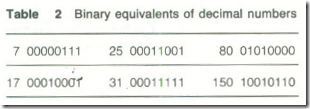
In digital electronic systems, the devices have two stable states, ON and OFF, and for this reason the binary number system is used. In the binary system only two digits 0 and 1 exist. Larger numbers are obtained by utilizing the powers of two. The digit at the right-hand side of a binary number represents a multiple (0 or 1) of 20; the next digit to the left represents a multiple of 21; and so on as shown by Table 1. The binary digits are generally known as bits.The value of each power of two is given in the table and any desired number can be attained by a correct choice of zeros and ones. Thus. number 18 for example: 18 is equal to 16 plus 2 and is therefore given by 0010010 in a 7-bit code or by 10010 if only 5 bits are used. Reading from the right (the least significant bit or Ɩsb), the number consists of zero 1, one 2, zero 4, zero 8 and one 16. Similarly, the binary equivalents of some other numbers are given in Table 2, assuming an 8-bit code.
Some typical examples of digital systems are the following: (a) the digital computer, and communication with a computer over telephone
Table 1 Binary code
Table 2 Binary equivalents of decimal numbers
lines; (b) the control of traffic lights, of lifts in tall buildings, of conveyor belts in factories, etc.; (c) safety arrangements for cranes and, various factory machines; (d) electronic counting systems such as counting the number of cars in a car park; (e) digital voltmeters; (f) digital watches; and (g) pocket calculators.
Combinational Logic
Combinational logic circuits are digital circuits the states of whose Outputs depend on the present logic states of the inputs. A combina-tional logic circuits is unable to store any information , and combina-tional logic circuits is often made by the interconnection of a number of gates.
An electronic gate is a logic element which is able to operate on an applied binary digital signal in a manner determined by its logical function. Seven different types of gate feature in digital circuitry, these are (i) the AND gate, (ii) the OR gate, (iii) the NOT gate, (iv) the NOR gate, (v) the NAND gate, (vi) the exclusive-OR gate and (vii) the exclusive-NOR gate.
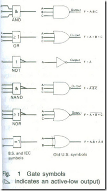
The British Standards Institution (BSI) and International Electrotechnical Commission (IEC) symbols for the various gates are given in Fig .1. The old American gate symbols which are often used are also shown in Fig .1.
Modem logic circuitry is invariably produced using integrated circuit technology. The majority of digital ICs belong to either the CMOS or the TTL logic families. The latter family has several subgroups of which me most popular is known as low-power Schottky TTL. The use of ICs for electronic equipment results in greater reliability and lower costs and allows complex circuit functions to be economically produced. Because of this, complex circuitry, such as is used in quartz watches, pocket calculators and home computers, has become relatively inexpensive and is commonly employed.
In both the CMOS and the TTL families, a standard package may accommodate more than one gate.
The NOT Gate
The NOT gate, or inverter, is used to invert a logic term, e.g. change logical 0 into logical 1 or to change 1 to 0. In a Boolean expression the NOT logical function is indicated by a bar placed over a symbol. Thus Ā means ‘NOT A’.
The NOT function is provided in both the CMOS and the TTL logic families by a hex inverter. This device, for example the TTL 7404, consists of six independent inverters or NOT gates in the one IC package.
The AND Gate
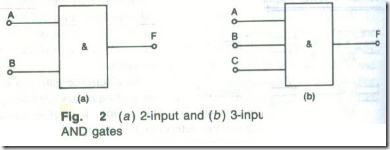
The AND gate is a logic circuit having two, or more, input terminals, labelled A, B, C, etc., and a single output terminal, usually labelled F. The output F of an AND gate is HIGH, or at logical I, only if all of its inputs are HIGH, or at logical 1. If any one, or more, of the inputs are LOW, or at logical 0, then the output of the circuit will be LOW, or at logical 0.
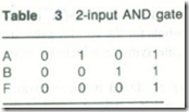
The symbols for 2-input and 3-input AND gates are shown in Fig .2. The logical operation of the gate can be described by a truth table. The truth table of a logic circuit shows the logical state of the output of the circuit for all the possible combinations of the logical states of the inputs to the circuit.
Table 3 gives the truth table for the 2-input AND gate. The logical operation of a gate can also be described by writing down its Boolean equation. For the 2-input AND gate this equation is
F = A.B (8.1)
The Boolean symbol for the AND logical function is the dot. Very often the dot is omitted and the equation is written as
F = AB (8.2)
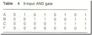
The number of columns in a truth table is equal to 2n, where n is the number of inputs. For the 2-input gate n = 2 and so there are 22 or 4 columns in Table 3. The truth table for a 3-input AND gate
must have 23 or 8 columns and it is given by Table 4. The Boolean equation for the 3-input AND gate is given by equation (8.3), i.e.
F = ABC (8.3)
Several different TTL circuits provide the AND gate function:
7408: quad 2-input AND gates
7411: triple 3-input AND gates
7421: dual 4-inpul AND gales.
The pin connections of the first two of these ICs are given in Fig .11.
Example 1
(a) How many input combinations are there for a 4-input AND gate? (b) How many inputs must be (i) al binary I for the output to also be at 1 . (ii) at binary 0 for the output to be at 0? (c) Write down the Boolean equation for the gate.
Solution
(a) Number of input combinations = 24 = 16 (Ans.)
(b) (i) All four, (ii) Just one (Ans.)
(c) F = ABCD (Ans.)
The OR Gate
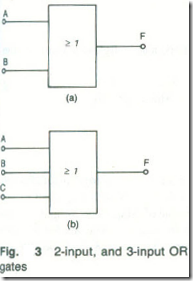
The OR gate, Fig .3. has its output Fat the logical 1 level whenever any one, or more, of its inputs are at logical 1. The output of the gate will be at logical 0 only if al] of its inputs are at logical 0. Table 5 gives the truth tables for 2-input and 3-input OR gates. The Boolean equations for each gate are given by equations (8.4) and (8.5) respectively, i.e.
F = A + B (8.4)
F = A + B+ C (8.5)
Note that the symbol for the OR logical function is the + sign.
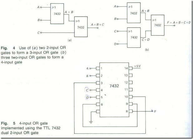
There is only one OR gate in most of the TTL logic sub-far and this is the 7432 quad 2-input OR gate. If a 3-input or a 4-input OR gate is wanted then two 2-input OR gates must be combined as shown by Fig .4. In figure (a) two, and in figure (b) one, of the OR gates is left unused.
Referring to Fig .11 for the pin connections of the 7432, the wiring of the 4-input OR gate circuit is as shown by Fig. 5.


