The Bipolar Junction Transistor
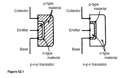
The bipolar junction transistor consists of three regions of semiconductor material. One type is called a p-n-p transistor, in which two regions of p-type material sandwich a very thin layer of n-type material. A second type is called an n-p-n transistor, in which two regions of n-type material sandwich a very thin layer of p-type material. Both of these types of transistors consist of two p-n junctions placed very close to one another in a back-to-back arrangement on a single piece of semiconductor material. Diagrams depicting these two types of transistors are shown in Figure 52.1.
The two p-type material regions of the p-n-p transistor are called the emitter and collector and the n-type material is called the base. Similarly, the two n-type material regions of the n-p-n transistor are called the emitter and collector and the p-type material region is called the base, as shown in Figure 52.1.
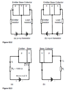
Transistors have three connecting leads and in operation an electrical input to one pair of connections, say the emitter and base connections can control the output from another pair, say the collector and emitter connections. This type of operation is achieved by appropriately biasing the two internal p-n junctions. When batteries and resistors are connected to a p-n-p transistor, as shown in Figure 52.2(a), the base-emitter junction is forward biased and the base-collector junction is reverse biased.
Similarly, an n-p-n transistor has its base-emitter junction forward biased and its base-collector junction reverse biased when the batteries are connected as shown in Figure 52.2(b).
For a silicon p-n-p transistor, biased as shown in Figure 52.2(a), if the base-emitter junction is considered on its own, it is forward biased and a
current flows. This is depicted in Figure 52.3(a). For example, if RE is 1000 Q, the battery is 4.5 V and the voltage drop across the junction is taken as 0.7 V, the current flowing is given by ![]()
When the base-collector junction is considered on its own, as shown in Figure 52.3(b), it is reverse biased and the collector current is something less than 1 µA.
However, when both external circuits are connected to the transistor, most of the 3.8 mA of current flowing in the emitter, which previously flowed from the base connection, now flows out through the collector connection due to transistor action.
Transistor Action
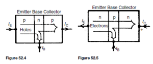
In a p-n-p transistor, connected as shown in Figure 52.2(a), transistor action is accounted for as follows:
(a) The majority carriers in the emitter p-type material are holes
(b) The base-emitter junction is forward biased to the majority carriers and the holes cross the junction and appear in the base region
(c) The base region is very thin and is only lightly doped with electrons so although some electron-hole pairs are formed, many holes are left in the base region
(d) The base-collector junction is reverse biased to electrons in the base region and holes in the collector region, but forward biased to holes in the base region; these holes are attracted by the negative potential at the collector terminal
(e) A large proportion of the holes in the base region cross the base-collector junction into the collector region, creating a collector current; conventional current flow is in the direction of hole movement
The transistor action is shown diagrammatically in Figure 52.4. For transistors having very thin base regions, up to 99.5% of the holes leaving the emitter cross the base collector junction.
In an n-p-n transistor, connected as shown in Figure 52.2(b), transistor action is accounted for as follows:
(a) The majority carriers in the emitter p-type material are electrons
(b) The base-emitter junction is forward biased to these majority carriers and electrons cross the junction and appear in the base region
(c) The base region is very thin and only lightly doped with holes, so some recombination with holes occurs but many electrons are left in the base region
(d) The base-collector junction is reverse biased to holes in the base region and electrons in the collector region, but is forward biased to electrons in the base region; these electrons are attracted by the positive potential at the collector terminal
(e) A large proportion of the electrons in the base region cross the base- collector junction into the collector region, creating a collector current
The transistor action is shown diagrammatically in Figure 52.5. As stated earlier, conventional current flow is taken to be in the direction of hole flow, that is, in the opposite direction to electron flow, hence the directions of the conventional current flow are as shown in Figure 52.5.
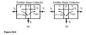
For a p-n-p transistor, the base-collector junction is reverse biased for majority carriers. However, a small leakage current, ICBO flows from the base to the collector due to thermally generated minority carriers (electrons in the collector and holes in the base), being present.
The base-collector junction is forward biased to these minority carriers. If a proportion, ˛, (having a value of up to 0.995 in modern transistors), of the holes passing into the base from the emitter, pass through the base-collector junction, then the various currents flowing in a p-n-p transistor are as shown in Figure 52.6(a).
Similarly, for an n-p-n transistor, the base-collector junction is reversed biased for majority carriers, but a small leakage current, ICBO flows from the collector to the base due to thermally generated minority carriers (holes in the collector and electrons in the base), being present. The base-collector junction is forward biased to these minority carriers. If a proportion, ˛, of the electrons passing through the base-emitter junction also pass through the base-collector junction then the currents flowing in an n-p-n transistor are as shown in Figure 52.6(b).
Transistor Symbols
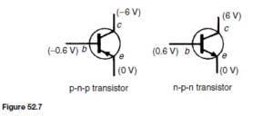
Symbols are used to represent p-n-p and n-p-n transistors in circuit diagrams and are as shown in Figure 52.7. The arrowhead drawn on the emitter of the symbol is in the direction of conventional emitter current (hole flow). The potentials marked at the collector, base and emitter are typical values for a silicon transistor having a potential difference of 6 V between its collector and its emitter.
The voltage of 0.6 V across the base and emitter is that required to reduce the potential barrier and if it is raised slightly to, say, 0.62 V, it is likely that the collector current will double to about 2 mA. Thus a small change of voltage between the emitter and the base can give a relatively large change of current in the emitter circuit; because of this, transistors can be used as amplifiers.
Transistor Connections
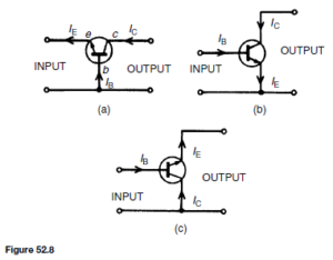
There are three ways of connecting a transistor, depending on the use to which it is being put. The ways are classified by the electrode that is common to both the input and the output. They are called:
(a) common-base configuration, shown in Figure 52.8(a)
(b) common-emitter configuration, shown in Figure 52.8(b)
(c) common-collector configuration, shown in Figure 52.8(c)
These configurations are for an n-p-n transistor. The current flows shown are all reversed for a p-n-p transistor.
Transistor Characteristics
The effect of changing one or more of the various voltages and currents associated with a transistor circuit can be shown graphically and these graphs are called the characteristics of the transistor. As there are five variables (collector, base and emitter currents, and voltages across the collector and base and emitter and base) and also three configurations, many characteristics are possible. Some of the possible characteristics are given below.
(a) Common-base configuration
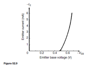
(i) Input characteristic. With reference to Figure 52.8(a), the input to a common-base transistor is the emitter current, IE, and can be varied by altering the base emitter voltage VEB . The base-emitter junction is essentially a forward biased junction diode, so as VEB is varied, the current flowing is similar to that for a junction diode, as shown in Figure 52.9 for a silicon transistor. Figure 52.9 is called the input characteristic for an n-p-n transistor having common-base configuration. The variation of the collector-base voltage VCB has little effect on the characteristic. A similar characteristic can be obtained for a p-n-p transistor, these having reversed polarities.
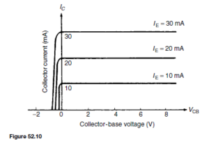
(ii) Output characteristics. The value of the collector current IC is very largely determined by the emitter current, IE. For a given value of IE the collector-base voltage, VCB, can be varied and has little effect on the value of IC. If VCB is made slightly negative, the collector no longer attracts the majority carriers leaving the emitter and IC falls rapidly to zero. A family of curves for various values of IE are possible and some of these are shown in Figure 52.10. Figure 52.10 is called the output characteristics for an n-p-n transistor having common-base configuration. Similar characteristics can be obtained for a p-n-p transistor, these having reversed polarities.
(b) Common-emitter configuration
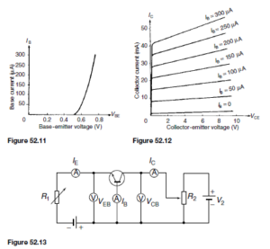
(i) Input characteristic. In a common-emitter configuration (see Figure 52.8(b)), the base current is now the input current. As VEB is varied, the characteristic obtained is similar in shape to the input characteristic for a common-base configuration shown in Figure 52.9, but the values of current are far less. With reference to Figure 52.6(a), as long as the junctions are biased as described, the three currents IE, IC and IB keep the ratio I : ˛: (I ð ˛), whichever configuration is adopted. Thus the base current changes are much smaller than the corresponding emitter current changes and the input characteristic for an n-p-n transistor is as shown in Figure 52.11. A similar characteristic can be obtained for a p-n-p transistor, these having reversed polarities.
(ii) Output characteristics. A family of curves can be obtained, depending on the value of base current IB and some of these for an n-p-n transistor are shown in Figure 52.12. A similar set of characteristics can be obtained for a p-n-p transistor, these having reversed polarities. These characteristics differ from the common base output characteristics in two ways:
(a) the collector current reduces to zero without having to reverse the collector voltage, and
(b) the characteristics slope upwards indicating a lower output resistance (usually kilohms for a common-emitter configuration compared with megohms for a common-base configuration).
A circuit diagram for obtaining the input and output characteristics for an n-p-n transistor connected in common-base configuration is shown in Figure 52.13. The input characteristic can be obtained by varying R1, which varies VEB , and noting the corresponding values of IE. This is repeated for various values of VCB. It will be found that the input characteristic is almost independent of VCB and it is usual to give only one characteristic, as shown in Figure 52.9.
To obtain the output characteristics, as shown in Figure 52.10, IE is set to a suitable value by adjusting R1. For various values of VCB, set by adjusting R2, IC is noted. This procedure is repeated for various values of IE. To obtain the full characteristics, the polarity of battery V2 has to be reversed to reduce IC to zero. This must be done very carefully or else values of IC will rapidly increase in the reverse direction and burn out the transistor.
The Transistor as an Amplifier
The amplifying properties of a transistor depend upon the fact that current flowing in a low-resistance circuit is transferred to a high-resistance circuit with negligible change in magnitude. If the current then flows through a load resistance, a voltage is developed. This voltage can be many times greater than the input voltage that caused the original current flow.
(a) Common-base amplifier
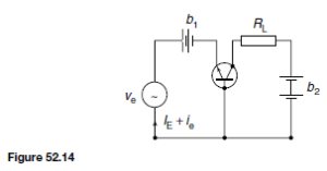
The basic circuit for a transistor is shown in Figure 52.14 where an n-p- n transistor is biased with batteries b1 and b2 . A sinusoidal alternating input signal, ve, is placed in series with the input bias voltage, and a load resistor, RL ,
is placed in series with the collector bias voltage. The input signal is therefore the sinusoidal current ie resulting from the application of the sinusoidal voltage ve superimposed on the direct current IE established by the base-emitter voltage VBE.
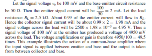
Let the signal voltage ve be 100 mV and the base-emitter circuit resistance
(b) Common-emitter amplifier
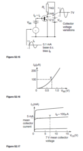
The basic circuit arrangement of a common-emitter amplifier is shown in Figure 52.15. Although two batteries are shown, it is more usual to employ only one to supply all the necessary bias. The input signal is applied between base and emitter, and the load resistor RL is connected between collector and emitter. Let the base bias battery provides a voltage which causes a base current IB of 0.1 mA to flow. This value of base current determines the mean
d.c. level upon which the a.c. input signal will be superimposed. This is the
d.c. base current operating point.
Let the static current gain of the transistor, ˛E, be 50. Since 0.1 mA is the steady base current, the collector current IC will be ˛E ð IB D 50 ð 0.1 D 5 mA. This current will flow through the load resistor RL (D 1 kQ), and there will be a steady voltage drop across RL given by IC RL D 5 ð 10ð3 ð 1000 D 5 V. The voltage at the collector, VCE, will therefore be VCC ð IC RL D 12 ð 5 D 7 V. This value of VCE is the mean (or quiescent) level about which the output signal voltage will swing alternately positive and negative. This is the collector voltage d.c. operating point. Both of these d.c. operating points can be pin-pointed on the input and output characteristics of the transistor. Figure 52.16 shows the IB /VBE characteristic with the operating point X positioned at IB D 0.1 mA, VBE D 0.75 V, say.
Figure 52.17 shows the IC/VCE characteristics, with the operating point Y positioned at IC D 5 mA, VCE D 7 V. It is usual to choose the operating points Y somewhere near the centre of the graph.
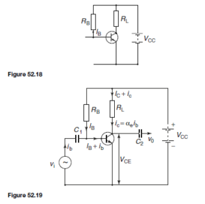
It is possible to remove the bias battery VBB and obtain base bias from the collector supply battery VCC instead. The simplest way to do this is to connect a bias resistor RB between the positive terminal of the VCC supply and the base as shown in Figure 52.18. The resistor must be of such a value that it allows 0.1 mA to flow in the base-emitter diode.
For a silicon transistor, the voltage drop across the junction for forward bias conditions is about 0.6 V. The voltage across RB must then be 12 – 0.6 =11.4 V. Hence, the value of RB must be such that IB x RB = 11.4 V, i.e. ![]() With the inclusion of the 1 kQ load resistor, RL , a steady 5 mA collector current, and a collector-emitter voltage of 7 V, the d.c. conditions are established.
With the inclusion of the 1 kQ load resistor, RL , a steady 5 mA collector current, and a collector-emitter voltage of 7 V, the d.c. conditions are established.
An alternating input signal (vi) can now be applied. In order not to disturb the bias condition established at the base, the input must be fed to the base by way of a capacitor C1. This will permit the alternating signal to pass to the base but will prevent the passage of direct current. The reactance of this capacitor must be such that it is very small compared with the input resistance of the transistor. The circuit of the amplifier is now as shown in Figure 52.19. The a.c. conditions can now be determined.
When an alternating signal voltage v1 is applied to the base via capacitor C1 the base current ib varies. When the input signal swings positive, the base current increases; when the signal swings negative, the base current decreases. The base current consists of two components: IB , the static base bias established by RB , and ib , the signal current. The current variation ib will in turn vary the collector current, iC . The relationship between iC and ib is given by
iC = ˛e ib , where ˛e is the dynamic current gain of the transistor and is not quite the same as the static current gain ˛E; the difference is usually small enough to be insignificant.
The current through the load resistor RL also consists of two components: IC, the static collector current, and iC, the signal current. As ib increases, so does iC and so does the voltage drop across RL . Hence, from the circuit:
The d.c. components of this equation, though necessary for the amplifier to operate at all, need not be considered when the a.c. signal conditions are being examined. Hence, the signal voltage variation relationship is:
the negative sign being added because vce decreases when ib increases and vice versa. The signal output and input voltages are of opposite polarity i.e.
a phase shift of 180° has occurred. So that the collector d.c. potential is not passed on to the following stage, a second capacitor, C2 , is added as shown in Figure 52.19. This removes the direct component but permits the signal voltage vo = iC RL to pass to the output terminals.
The Load Line
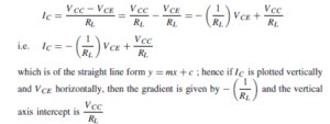
The relationship between the collector-emitter voltage (VCE) and collector current (IC) is given by the equation: VCE = VCC – ICRL in terms of the d.c. conditions. Since VCC and RL are constant in any given circuit, this represents the equation of a straight line which can be written in the y D mx C c form. Transposing VCE = VCC – ICRL for IC gives:
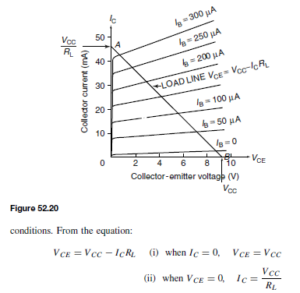
A family of collector static characteristics drawn on such axes is shown in Figure 52.12 on page 318, and so the line may be superimposed on these as shown in Figure 52.20.
The reason why this line is necessary is because the static curves relate IC to VCE for a series of fixed values of IB . When a signal is applied to the base of the transistor, the base current varies and can instantaneously take any of the values between the extremes shown. Only two points are necessary to draw the line and these can be found conveniently by considering extreme
Thus the points A and B respectively are located on the axes of the IC/VCE characteristics. This line is called the load line and it is dependent for its position upon the value of VCC and for its gradient upon RL . As the gradient is given by ![]() , the slope of the line is negative.
, the slope of the line is negative.
For every value assigned to RL in a particular circuit there will be a corresponding (and different) load line. If VCC is maintained constant, all the possible lines will start at the same point (B) but will cut the IC axis at different points A. Increasing RL will reduce the gradient of the line and vice-versa. Quite clearly the collector voltage can never exceed VCC (point B) and equally the collector current can never be greater than that value which would make VCE zero (point A).
Using the circuit example of Figure 52.15, we have
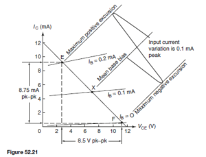
The load line is drawn on the characteristics shown in Figure 52.21, which we assume are characteristics for the transistor used in the circuit of Figure 52.15 earlier. Notice that the load line passes through the operating point X, as it should, since every position on the line represents a relationship between VCE and IC for the particular values of VCC and RL given. Suppose
that the base current is caused to vary š0.1 mA about the d.c. base bias of 0.1 mA. The result is IB changes from 0 mA to 0.2 mA and back again to 0 mA during the course of each input cycle. Hence the operating point moves up and down the load line in phase with the input current and hence the input voltage. A sinusoidal input cycle is shown on Figure 52.21.
Current and Voltage Gains
The output signal voltage (vce) and current (iC) can be obtained by projecting vertically from the load line on to VCE and IC axes respectively. When the input current ib varies sinusoidally as shown in Figure 52.21, then vce varies sinusoidally if the points E and F at the extremities of the input variations are equally spaced on either side of X.
The peak to peak output voltage is seen to be 8.5 V, giving an r.m.s. value of ![]() The peak-to-peak output current is 8.75 mA, 2 giving an r.m.s. value of 3.1 mA. From these figures the voltage and current amplifications can be obtained.
The peak-to-peak output current is 8.75 mA, 2 giving an r.m.s. value of 3.1 mA. From these figures the voltage and current amplifications can be obtained.
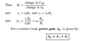
The dynamic current gain Ai (D˛e ) as opposed to the static gain ˛E, is given by:
This always leads to a different figure from that obtained by the direct division of ![]() which assumes that the collector load resistor is zero. From Figure 52.21 the peak input current is 0.1 mA and the peak output current is
which assumes that the collector load resistor is zero. From Figure 52.21 the peak input current is 0.1 mA and the peak output current is
This cannot be calculated from the data available, but if we assume that the base current flows in the input resistance, then the base voltage can be determined. The input resistance can be determined from an input characteristic such as was shown earlier.
Thermal Runaway
When a transistor is used as an amplifier it is necessary to ensure that it does not overheat. Overheating can arise from causes outside of the transistor itself, such as the proximity of radiators or hot resistors, or within the transistor as the result of dissipation by the passage of current through it. Power dissipated within the transistor, which is given approximately by the product IC VCE, is wasted power; it contributes nothing to the signal output power and merely raises the temperature of the transistor. Such overheating can lead to very undesirable results.
The increase in the temperature of a transistor will give rise to the production of hole electron pairs, hence an increase in leakage current represented by the additional minority carriers. In turn, this leakage current leads to an increase in collector current and this increases the product IC VCE. The whole effect thus becomes self-perpetuating and results in thermal runaway. This rapidly leads to the destruction of the transistor.
Two basic methods of preventing thermal runaway are available and either or both may be used in a particular application:
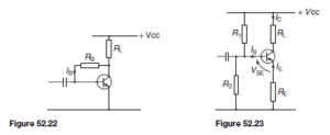
Method 1. The use of a single biasing resistor RB as shown earlier in Figure 52.18 is not particularly good practice. If the temperature of the transistor increases, the leakage current also increases. The collector current, collector voltage and base current are thereby changed, the base current decreasing as
IC increases. An alternative is shown in Figure 52.22. Here the resistor RB is returned, not to the VCC line, but to the collector itself.
If the collector current increases for any reason, the collector voltage VCE will fall. Therefore, the d.c. base current IB will fall, since ![]() . Hence the collector current IC D ˛EIB will also fall and compensate for the original increase.
. Hence the collector current IC D ˛EIB will also fall and compensate for the original increase.
A commonly used bias arrangement is shown in Figure 52.23. If the total resistance value of resistors R1 and R2 is such that the current flowing through the divider is large compared with the d.c. bias current IB , then the base voltage VBE will remain substantially constant regardless of variations in collector current. The emitter resistor RE in turn determines the value of emitter current which flows for a given base voltage at the junction of R1 and R2. Any increase in IC produces an increase in IE and a corresponding increase in the voltage drop across RE. This reduces the forward bias voltage VBE and leads to a compensating reduction in IC
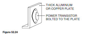
Method 2. This method concerns some means of keeping the transistor temperature down by external cooling. For this purpose, a heat sink is employed, as shown in Figure 52.24 If the transistor is clipped or bolted to a large conducting area of aluminium or copper plate (which may have cooling fins), cooling is achieved by convection and radiation.
Heat sinks are usually blackened to assist radiation and are normally used where large power dissipation’s are involved. With small transistors, heat sinks are unnecessary. Silicon transistors particularly have such small leakage cur- rents that thermal problems rarely arise.

