encoder
In this encyclopedia, an encoder is a digital chip that converts a decimal-valued input into a binary-coded output.
The term “encoder” may alternatively refer to a rotational encoder (also known as a rotary encoder) which has a separate entry in Volume 1 of this encyclopedia. The term may also describe a code hopping encoder, which is an encryption device used in keyless entry systems for automobiles.
What It Does
An encoder is a logic chip that receives an input consisting of an active logical state on one of at least four input pins, which have decimal values from 0 upward in increments of 1. The encoder converts the active pin number into a binary value represented by logic states on at least two output pins. This behavior is opposite to that of a decoder.
Encoders are identified in terms of their inputs and outputs. For example:
• 4-to-2 encoder (four input pins, two output pins)
• 8-to-3 encoder (eight input pins, three out- put pins)
• 16-to-4 encoder (sixteen input pins, four out- put pins)
In the early days of computing, encoders processed interrupts. This application is now rare, and relatively few encoder chips are still being manufactured. However, they are still useful in small devices—for example, if a large number of inputs must be handled by a microcontroller that has insufficient pins to receive data from each individually.
Schematic Symbol
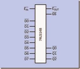
Like other logic-based components, the encoder does not have a specific schematic symbol and can be represented by a plain rectangle as in Figure 14-1, with inputs on the left and outputs on the right. The bars printed above some of the abbreviations indicate that an input or output is active-low. In this chip, the 74LS148, all inputs and outputs are active-low.
Generally speaking, inputs labeled D0, D1, D2… are used for data input, although they may simply be numbered, with no identifying letter. The encoded outputs are typically identified as Q0, Q1, Q2… or A0, A1, A2… with Q0 or A0 designating the least significant bit in the binary number.
Pins labeled E and GS are explained in the following section.
Figure 14-1. While no specific schematic symbol exists for an encoder chip, this style is commonly used. Shown here is a 16–to–4 encoder with active-low inputs and outputs.
Similar Devices
The similarities and differences between encoder, decoder, multiplexer, and demultiplexer can cause confusion.
• In an encoder, an active logic state is applied to one of four or more input pins, while the rest remain in an inactive logic state. The in- put pin number is converted to a binary code which is expressed as a pattern of logic states on two or more output pins.
• In a decoder, a binary number is applied as a pattern of logic states on two or more input pins. This value determines which one of four or more output pins will have an active logic state, while the rest remain in an inactive logic state.
• A multiplexer can connect a choice of multiple inputs to a single output, for data transfer. The logic state of an enable pin, or a bi- nary number applied as a pattern of logic states to multiple control pins, chooses which input should be connected with the output pin. The alternative term data selector evokes the function of this device more clearly.
• An analog multiplexer may allow its inputs and outputs to be swapped, in which case it becomes a demultiplexer. It can connect a single input to one of multiple outputs, for data transfer. The logic state of an enable pin, or a binary number applied as a pattern of logic states to multiple control pins, chooses which output should be used. The alternative term data distributor evokes the function of this device more clearly.
How It Works
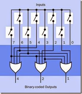
An encoder contains logic gates. The internal logic of an 8-to-3 encoder is shown in Figure 14-2, where the darker blue rectangle rep- resents the chip. The switches in this figure are external and are included only to clarify the concept. An open switch is imagined to provide an inactive logic input, while a single closed switch provides an active logic input. (Multiple active inputs can be handled by a priority encoder, de- scribed below).
Each input switch has a numeric status from 1 to
7. The switch with value 0 does not make an internal connection, because the output from the OR gates is 000 by default.
The logic state of each OR output represents a binary number, weighted with decimal values 1, 2, and 4, as shown at the bottom of the figure. Thus, if switch 5 is pressed, by tracing the connections it is clear that the outputs of OR gates 4 and 1 become active, while the output from gate 2 remains inactive. The values of the active out- puts thus sum to 5 decimal.
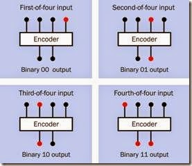
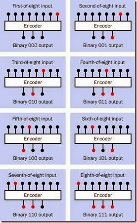
Figure 14-3 shows the outputs for all possible in- put states of a 4-to-2 encoder. Figure 14-4 shows the outputs for all possible input states of an 8- to-3 encoder. These diagrams assume that a high logic state is an active logic state, on input or output. This is usually the case.
Figure 14-2. A simplified simulation of the internal logic of an 8-to-3 encoder. The dark blue rectangle indicates the space inside the chip. The external switches are in- cluded only to clarify the concept. An encoder chip would have an Enable line to create an active output.
Figure 14-3. The four possible inputs of a 4-to-2 encoder (top of each panel) and the encoded outputs (below).
Figure 14-4. The eight possible inputs of an 8-to-3 en- coder (at the top of each panel), and the encoded outputs (below). Note that one input of an encoder must always be logic-high. All logic-low inputs are not a valid state.
Unlike ripple counters, where propagation de- lays can reduce the overall response time of the component, decoders respond within two or three nanoseconds.
Variants
A simple encoder assumes that only one input pin can be logically active at a time. A priority encoder assigns priority to the highest-value input pin if more than one happens to receive an active input. It ignores any lower-value inputs. An ex- ample is the 74LS148, which is an 8-to-3 chip.
A few encoders feature three-state outputs (also known as tri-state), in which a high-impedance or “floating” output state is available in addition to the usual high and low logic states. The high- impedance state allows multiple chips to share an output bus, as those that are in high- impedance mode appear to be disconnected. This is useful if two or more encoders are cascaded to handle a larger number of inputs.
Values
As is the case with other logic chips, most en- coders in the through-hole 74xx series are in- tended for 5VDC power supply while the older 4000 series may tolerate up to 18VDC. Surface- mount versions may use voltages as low as 2VDC.
See the section on logic gates in Chapter 10 for a discussion of acceptable high and low input states. On the output side, the 4000 series chips are able to source less than 1mA at 5VDC, but the 74HCxx series can manage around 20mA.
How to Use It
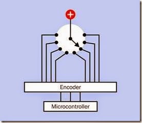
Suppose that a microcontroller should respond to an eight-position rotary switch. Because the switch cannot be turned to more than one position at a time, all of its eight contacts can be connected with the inputs on an encoder, which will deliver a 3-bit binary number to three inputs of the microcontroller. Code inside the microcontroller then interprets the pin states.
This is shown in Figure 14-5. Pulldown resistors would be needed on the input pins of the en- coder, to prevent them from floating when they are not connected by the rotary switch. They have been omitted from this diagram for simplicity. Debouncing the switch would be handled by the microcontroller.
Other forms of input may be used instead of a rotary switch. For example, the outputs from eight comparators or eight phototransistors could be passed through an encoder.
Figure 14-5. Output from an eight-input rotary switch could be connected through an 8-to-3 encoder to provide input to a microcontroller using a reduced number of pins. Pulldown resistors have been omitted for simplicity.
Cascaded Encoders
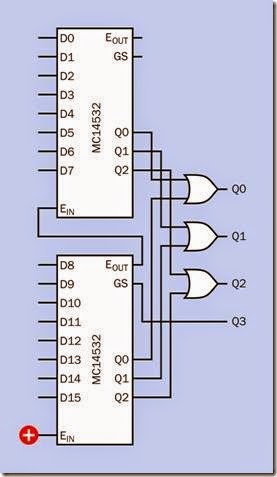
Encoders are often provided with features to facilitate handling additional inputs via multiple chips. Typically, a second Enable pin is provided, as an output that connects with the Enable input of the preceding chip. This preserves the priority function, so that an input on the second chip prevents any additional input to the first chip from affecting the output. In a datasheet, the en- able pins may be labeled EIN and EOUT, or EI and EO.
In addition, a GS pin will be included, meaning “Group Select.” It is logically active only when the encoder is enabled and at least one input is active. The GS pin of the most-significant encoder provides an additional binary digit.
The outputs from two encoders can be linked via OR gates, as shown in Figure 14-6, where the lower chip’s GS output provides the most significant bit of a four-bit binary number.
Figure 14-6. Two eight-bit encoders can be cascaded to handle 16 separate inputs. In this example, the encoders use active-high logic.
What Can Go Wrong
Problems that are common to all digital chips are summarized in the section on logic gates in “What Can Go Wrong” on page 105.
See “What Can Go Wrong” on page 149 in the entry describing decoders for a list of more specific problems that also afflict encoders.

