shift register
The term shift register is rarely hyphenated. In this encyclopedia, no hyphen is used.
A shift register can function as a queue, but this term is more usually applied to software. When the output from the last stage of a shift register is connected back to its input, it can function as a ring counter, but that application is described in the counter entry of this encyclopedia.
Component catalogs sometimes list shift registers as binary ripple counters, instead of giving them their own section. In this encyclopedia, a binary counter is considered to have binary-weighted outputs (with values 1, 2, 4, 8…. in decimal notation) and is de- scribed in the counter entry. A shift register has outputs that are not necessarily binary- weighted.
What It Does
A register is a component (or a small section of computer memory) that stores information. The smallest unit of information is one bit (i.e., one binary digit) with a value 1 or 0 that can be rep- resented by a high or low logic state. A shift register most commonly is designed to store eight bits, although some store four.
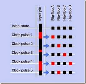
Each bit is memorized by the status of a flip- flop inside the register. For a detailed description of flip-flops, see Chapter 11. When a pulse from an external clock is received by the shift register, all of the bits in storage are moved along one step, from each flip-flop to the next. The high or low status of an input pin at that moment is clocked in to the first flip-flop, while the bit in the last flip-flop is overwritten by the bit preceding it. A diagram representing the function of a basic four-bit shift register is shown in Figure 12-1.
Note that the status of the input pin is ignored until the moment when a clock pulse copies it into the first flip-flop. In the figure, when the in- put pin has a brief high state that ends immediately before clock pulse three, the high state is ignored.
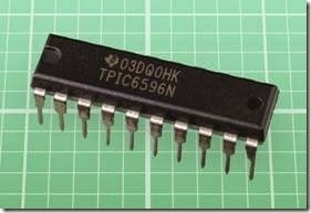
A shift-register chip is shown in Figure 12-2. Because the functionality of a shift register is now often incorporated in much larger logic chips, it is less widely used as a stand-alone component than it used to be. It is still useful for purposes of serial-parallel or parallel-serial conversion, and for small tasks such as scanning a matrix- encoded keyboard or keypad. It also has educational applications and can be used in conjunc- tion with a microcontroller.
Figure 12-1. The function of a four-bit shift register in which each flip-flop may be set to a high or a low state, represented here with red or black squares. After a high bit is clocked into the chip, it is moved one space along by each subsequent clock pulse.
Figure 12-2. This 8-bit shift-register chip is unusual in that it uses “power logic,” in which open-drain outputs en-
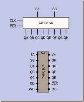
gram showing the physical chip and its pinouts. The meaning of the abbreviations identifying the inputs, outputs, and control functions will be de- scribed in “How It Works” on page 122.
Figure 12-3. Typical schematic representation of a shift register, compared with the pinouts of the actual component.
The schematic symbol representing a shift register may appear superficially similar to the phys- ical form of the chip which contains it, but the physical layout of the pins is unlikely to be the same.
How It Works
able it to drive relatively high-current devices. It can sink up to 250mA at each of its output pins, at up to 45VDC.
Schematic Representation
No specific symbol exists for a shift register. It is represented in a schematic by a simple rectangle, often (but not always) with control inputs on the left, data inputs arrayed along the upper edge, and data outputs along the lower edge. An ex- ample is shown in Figure 12-3, along with a dia- A shift register generally consists of a chain of D- type flip-flops. See the entry describing flip-flops in Chapter 11 for a detailed explanation of this component.
The simplest shift register functions as a serial-in, serial-out device, abbreviated with the acronym SISO. Because the first bit that enters it will be the first to leave at the opposite end, it can also be described as a first-in, first-out data storage de- vice, using the acronym FIFO.
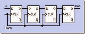
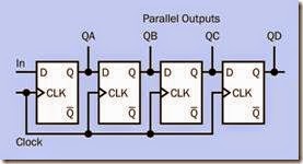
The basic connections between flip-flops in a four-bit SISO shift-register are shown in Figure 12-4. The D input in each section refers to the fact that it is a D-type flip-flop. The primary output from each flip-flop is identified with letter Q.
Figure 12-4. The simplest shift register is a serial-in, serial-out (SISO) device. This example contains four D- type flip-flops.
Each clock input is labeled CLK. When the output of each flip-flop is coupled to the input of the next flip-flop, and both share the same clock signal, the clock signal will cause the state of the third flip-flop to be sent to the fourth, the output of the second to be copied to the third, the out- put of the first to the second, and the input state will be copied to the first.
Abbreviations and Acronyms
The shift register will usually have an additional input that forces an immediate “clear” of all the registers, regardless of the clock state at that mo- ment. This input is usually labeled CLR and will have a bar printed above it if it is active-low (which is the usual convention). If there is a pin labeled MR (meaning “Master Reset”), it will have the same function as CLR.
Because its effect is independent of the clock state, the clear signal is described as an asynchronous input.
While the abbreviation CLK is frequently used to identify the clock input, SCLK is also used (meaning “serial clock”), and occasionally the abbreviation CP may be found, meaning “clock pulse”
input. If the shift register contains two stages, one to clock data in and the second to clock data out, they may be separately clocked, in which case they will be identified with different abbreviations. These are not standardized, but should be explained in the manufacturer’s datasheet. No matter which abbreviation is used for a clock input, it will have a bar printed above it if the in- put is active-low.
Shift registers are generally edge triggered, meaning that the rising or falling edge of a clock pulse triggers the bit-shifting operation. If the component responds to a clock transition from low to high, it is rising-edge triggered. If it responds to a transition from high to low, it is falling-edge triggered, and this may be indicated in the schematic by a small circle, properly known as a bubble, preceding the triangle which indicates that this is an edge-triggered device.
Most shift registers are positive-edge triggered.
Parallel Outputs and Inputs
In many shift registers, data may be read out in parallel (from all flip-flops simultaneously), using pins provided for this purpose. In this mode, the shift register can function as a serial-parallel con- verter (serial in, parallel out, represented by the acronym SIPO). A simplified schematic of the internal connections is shown in Figure 12-5.
Where parallel outputs are provided, they are often identified as QA, QB, QC, and so on (moving from left to right) but may alternatively be de- scribed as Q1, Q2, Q3, Q4, and so on.
In a schematic, the input pin is conventionally shown as being at the left end of the component. Often two inputs are provided, connected inter- nally as inputs to a NAND gate. The inputs are likely to be labeled A and B, but may alternatively be named SA and SB, indicating that they are serial inputs. S1 and S2 are alternative classifica- tions. If parallel inputs exist, they may be identified as PA, PB, PC, and so on.
Figure 12-5. Many shift registers have pins connected to points along the chain of flip-flops. These connections en- able data to be read from the shift register in parallel.
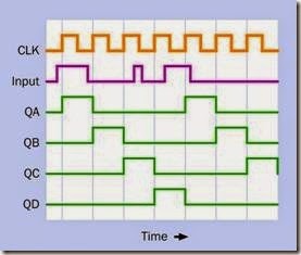
If serial data is supplied asynchronously, as in the illustration in Figure 12-1, it will be ignored until the shift register is triggered by the next clock pulse. The input state at that moment will then be copied into the first flip-flop, while the data that is already being stored in the shift register will be moved along the chain. In datasheets, this is customarily represented by a diagram such as the one in Figure 12-6. This diagram assumes that the shift-register is rising-edge triggered. Note that a brief fluctuation in the input which does not coincide with a clock-trigger event will be ignored.
Variants
Serial In, Serial Out
A basic SISO shift register allows only for serial input (at one end of the chain of flip-flops) and serial output (at the other end of the chain). No pins are available for parallel output of data.
This type of component usually permits 64-bit storage, where parallel output is simply impractical, as too many pins would be required. An ex- ample is the 4031B chip. This includes provision for recirculation of bits, so that it will also function as a ring counter (see Chapter 13 for a discussion of this function). As is always the case with logic chips, the part number will be preceded by letter(s) identifying the manufacturer, and a suffix will distinguish variants of the chip.
Another type of SISO shift register is programmable. It will store any number of bits from 1 through 64, determined by a binary number applied in the form of high/low states to five pins reserved for this purpose. An example is the 4557B.
Figure 12-6. In a rising-edge-triggered shift register, the high or low state of an asynchronous input (purple line) is copied into the first flip-flop of a shift register by each clock pulse (orange line). Brief fluctuations that do not coincide with a rising clock pulse are ignored. Existing data in the register is shifted from one flip-flop to the next.
Serial In, Parallel Out
The majority of serial-input shift registers allow parallel output from points along the chain in addition to serial output at the end of the chain. These chips almost all are 8-bit registers. Typically two inputs are provided, one of which can be used to receive bits that recirculate from the end of the chain, back to the beginning. Widely used examples are the 4094B and the 74×164, where an acronym identifying the logic family will be substituted for the x.
Parallel In, Serial Out
A minority of shift registers are able to function as parallel-serial converters (parallel in, serial out, represented by the acronym PISO). Typically this type of chip allows jam-type parallel data input, meaning that the data is forced into the flip-flops
via a separate pin for each of them. Parallel input is enabled by the status of a serial/parallel control pin. When the control pin reverts to its opposite status, each clock pulse will now shift data along the chain of flip-flops, allowing it to be read from the final output one bit at a time. Thus, data can be entered into the chip in parallel and read out of it serially. Examples are the 4014B and 4021B. Both are 8-bit.
Parallel In, Parallel Out
Shift registers that permit parallel output in addition to parallel input are almost all of the universal type, described in the next section.
Universal
A universal shift register is capable of all four modes of operation: SISO, SIPO, PISO, and PIPO. The four modes of the component are selected by the high or low status of two mode select pins. In addition, this component may have the ability to shift the register states either left or right. A bidirectional shift register has this same capabil- ity, and may also have PISO and PIPO capability, depending on the chip. Examples are the 74×195 and 74×299, where an acronym identifying the logic family will be substituted for the x in the number.
Universal shift registers are almost all 4-bit or 8- bit. They often have relatively complicated features, such as access to internal JK flip-flops, or pins that are multiplexed to provide different functionality depending whether an enable pin is held high or low. Datasheets must be checked carefully to ensure correct use.
Dedicated shift registers of SIPO or PISO type will be easier to use.
Values
As is the case with other logic chips, most flip- flops in the through-hole 74xx series are intend- ed for 5VDC power supply while the older 4000 series may tolerate up to 18VDC. Surface-mount versions may use voltages as low as 2VDC.
See the section on logic gates in Chapter 10 for a discussion of acceptable high and low logic- input states. On the output side, the 4000 series chips are able to source less than 1mA at 5VDC, but the 74HCxx series can usually manage around 20mA.
If a shift register is used for high-speed operation, the following values must be considered (identical notation, and similar values, are found in specifications for flip-flops):
• tS Setup time: The input state of a shift reg- ister must exist for a very brief period before the clock trigger that processes it. This peri- od is known as the setup time. In the 4000 series of chips, recommended setup may be as long as 120ns. The value will be much lower in 74xx chips.
• tH Hold time: The minimum time in nano- seconds for an input to persist after the ac- tive edge of a clock pulse that has processed it. In many shift registers, no hold time is nec- essary, as the chip has already been activated by the rising edge of the clock pulse.
• tCO Clock-to-output: The elapsed time after a clock trigger, before the output changes. This is a function of the internal workings of the chip, and may be broken down into low- to-high and high-to-low output transitions, as follows.
• TPLH Propagation to Low-to-High: The elapsed time after an active clock trigger, before a low-to-high swing occurs at an out- put. This may not be identical to TPHL.
• TPHL Propagation to High-to-Low: The elapsed time after an active clock trigger, before a high-to-low swing occurs at an out- put. This may not be identical to TPLH.
• fMAX Maximum clock frequency for reliable operation. In the older design of 4000 series chips, 3MHz may be recommended with a power supply of 5VDC. Higher frequencies are possible with a higher voltage power
supply. Frequencies as high as 20MHz are possible in the 5VDC 74HC00 series.
• tW(H) The minimum high clock pulse width in nanoseconds. In the older design of 4000 series chips, 180ns may be recommended with a power supply of 5VDC. Shorter pulses are possible with higher voltage power sup- ply. Pulses as short as 20ns are possible in the 5VDC 74HC00 series.
• tW(L) The minimum low clock pulse width in nanoseconds. This is likely to be the same as tW(H).
Power Considerations
Shift registers conform with the usual power- supply requirements for logic families. These are described in detail in the logic gate entry in Chapter 10. Likewise, the ability of a shift register to source or sink current is usually determined by its logic family. In a few cases, however, shift reg- isters have an additional open-drain output stage for each register, capable of sinking currents as high as 250mA. The Texas Instruments TPIC6596 shown in Figure 12-2 is an example. When an open-drain output is connected with a logic de- vice whose input cannot be allowed to float in- determinately, a pullup resistor must be added.
Three-State Output
A chip may have a three-state output (also known as tri-state output, a term which was trademarked puts of the shift register out of the circuit. Consequently, if other components sharing the bus are also in high-impedance output mode, the state of the bus will “float,” with uncertain results. To avoid this, a pullup resistor of 10K to 100K can be used on each bus-line.
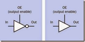
Where the internal components of a shift register are shown in a datasheet, a three-state output is usually represented with a buffer symbol or inverter symbol that has an additional control in- put located on its upper edge, as shown in Figure 12-7. This should not be confused with the similar placement of a positive power supply in- put to an amplifier or op-amp. (Schematics showing the interior elements of a logic chip almost never include power-supply connections.)
Figure 12-7. A shift register may be capable of a three- state output, where high impedance is an option addition- al to the usual high or low logic state. An output enable pin allows this. It is typically shown as an additional input to an inverter (left) or buffer (right) inside the shift-register chip.
How to Use It
but is now used generically). This means it will be capable of changing its outputs so that instead of sourcing or sinking current in a logical high or low state, they can have a high impedance. The chip then becomes “invisible” to others which may be sharing the same output bus. The high- impedance state is usually applied to all outputs from the shift register simultaneously when en- abled by a separate pin, often identified as OE, meaning output-enable. Examples of three-state shift registers are the 74×595 or the 4094B chip.
The high-impedance state can be thought of as being almost equivalent to switching the out- The SISO application of a shift register can be used simply to delay the transmission of data by storing it and moving it from one flip-flop to the next before it is read out of the end of the chain.
The SIPO application of a shift register (serial in, parallel out) may be useful where a microcontroller has insufficient outputs to control multiple devices. Serial data can be sent from a single microcontroller output to the input of a shift register. The chip can then drive a separate device from each of its parallel output pins. If there are eight devices, the microcontroller can send a sequence of eight bits, each of which will control the on/off status of one device when the bits are read out of the shift register in parallel. If more devices are used, an additional shift-register can be daisy-chained to the output from the first.
Clock signals can be supplied from the micro- controller, along with a signal to the clear input of the shift register, if desired. Alternatively, the old bit states in the shift register can simply be “clocked out” and replaced with a new set of serial data. During the process of “bit banging,” the parallel outputs of the shift register can remain connected directly with the output devices if the clock speed from the microcontroller is fast enough, as devices such as relays will not respond to extremely brief pulses.
For generic shift registers that do not have open- drain outputs, a buffer will be needed to provide sufficient current for any device using more cur- rent than an LED.
If a shift register is configured for PISO mode (parallel in, serial out) it can be placed on the in- put side of a microcontroller, polling a variety of devices and feeding their states into the micro- controller serially.
Dual Inputs
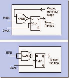
Where a shift register has two serial inputs (as is often the case), they are almost always linked as inputs to an internal NAND gate. This allows the output from the end of the chain of flip-flops to be connected back to the beginning of the chain, if the shift register is to function as a ring counter. However, if this function is not used and a single input is required, the two inputs to the shift register can be tied together. In this configuration, the input becomes active-low. The two possible configurations are shown in Figure 12-8. It is important never to leave an input floating, or un- connected.
Figure 12-8. Two possible configurations where a shift register allows two inputs linked with an internal NAND gate.
Preloading the Shift Register
Where a shift register will be used to output a single recirculating bit (or in similar applications), the component must be preloaded with a high state in its first register. This may require a one- shot (monostable) timer which is activated only when the circuit is powered up.
Polling a Keyboard
Two shift registers can be used to scan the data lines in a matrix-encoded keyboard or keypad. This is often known as polling the keyboard. Pro- vided the scan rate is sufficiently fast, the user experiences a seemingly immediate response to a key-press.
While the full schematic is too large and complex to be included here, many examples can be found online.
Arithmetical Operations
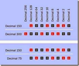
Shift registers were traditionally used to perform arithmetical operations on binary numbers. If the number is represented by eight bits (i.e., one byte) with the most significant digit on the left, shifting the bits one space to the right will have the effect of dividing the byte value by 2. If the bits are shifted one space to the left, the byte value will be multiplied by 2 (provided an additional register is available to store the most significant bit after it has been shifted). This concept is illustrated in Figure 12-9.
Figure 12-9. In the upper section of this diagram, a binary number represented by eight bits in a shift register is multiplied by 2 by shifting all the bits one space to the left. In the lower section, the same binary number is divided by 2 by shifting all the bits one space to the right. The binary values are shown in decimal notation to the left.
In the upper section of the figure, the binary number 10010110 (chosen arbitrarily) is represented in the eight flip-flops of a shift register. The decimal place value of each digit is indicated. Adding up the place values of the 1s in the number, the total is 128 + 16 + 4 + 2 = 150. Below the white line, the digits have been shifted one place to the left, with the leftmost digit carried over to an additional location, while a zero is inserted in the rightmost location. Assuming that the additional place at the leftmost location has a place value of 256, the total is now 256 + 32 + 8 + 4 = 300.
In the lower section of the figure, the same binary number has been shifted one space to the right, with a 0 introduced in the leftmost location. The decimal value is now 64 + 8 + 2 + 1 = 75.
While this application for shift registers was common during development of digital computing in the 1960s and 1970s, the shift register as a separate component became less common sub- sequently, as its functionality was acquired by modern CPU chips.
Buffering
A shift register may also be used as a buffer be- tween two circuits where the clock speeds are different. Digits are clocked in by the first circuit, then clocked out by the second. Some shift registers allow two clock inputs and can be used for this purpose.
What Can Go Wrong
Problems that tend to affect digital chips generally are listed in the entry on logic gates (see “What Can Go Wrong” on page 105).
Confusing Classification
Because of the functional similarity to a binary ripple counter, a shift register is sometimes listed by component suppliers as a counter. In fact, a binary counter will almost always have outputs that have place values 1, 2, 4, 8…. and upward, while the outputs from a shift register will not have place values.
When searching for a shift register, it can be found by specifying a “counting sequence” of serial to parallel, serial to serial, parallel to serial, or parallel to parallel. If the “counting sequence” is simply up or down, the component is a counter, not a shift register.
Inadequate Setup Time
Each flip-flop in a shift register must have a stable input state before the next triggering event shifts the data. If this setup time is reduced below the minimum specified in the datasheet, results will be unpredictable.
Unconnected Input
Because many shift registers have a choice of two inputs to the same chain of internal flip-flops, it is easy to leave one of them unconnected by accident. A floating input will be vulnerable to any stray electromagnetic fields, and is almost certain to create random effects.
Output Enable Issues
The output enable pin on a shift register that has three-state logic outputs is usually active-low. Consequently, if the pin is left unconnected, the logic outputs may go into high-impedance mode, or will fluctuate unpredictably. Where three-state outputs are not required, a safe course of action will be to avoid using three-state chips.
Floating Output Bus
If a pullup resistor is omitted from a bus that is shared by three-state chips, the results will be unpredictable. Even if the circuit design seems to guarantee that at least one chip will have a high or low output on the bus, a pullup resistor should still be included.

