SCR
The acronym SCR is derived from silicon-controlled rectifier, which is a gate-triggered type of thyristor. A thyristor is defined here as a semiconductor having four or more alternating layers of p-type and n-type silicon. Because it predated integrated circuits, and in its basic form consists of a single multilayer semiconductor, a thyristor is considered to be a discrete component in this encyclopedia. When a thyristor is combined with other components in one package (as in a solid-state relay), it is considered to be an integrated circuit.
Other types of thyristor are the diac and triac, each of which has its own entry. Thyristor variants that are not so widely used, such as the gate turn-off thyristor (GTO) and silicon-controlled switch (SCS), do not have entries here.
In the 1920s, the thyratron was a gas-filled tube that functioned as a switch and a rectifier. In 1956, General Electric introduced a solid-state version of it under the name thyristor. In both cases, the names were derived from the thyroid gland in the human body, which controls the rate of consumption of energy. The thyratron and, subsequently, the thyristor enabled control of large flows of current.
The SCR (silicon-controlled rectifier) is a type of thyristor, although the two terms are often used as if they are synonymous. Text that refers loosely to a thyristor may actually be discussing an SCR, and vice versa. In this encyclopedia, the SCR, di- ac, and triac are all considered to be variant types of thyristor.
An SCR is a solid-state switch that in many in- stances can pass high currents at high voltages.
Like a bipolar transistor, it is triggered by volt- age applied to a gate. Unlike the transistor, it al- lows the flow of current to continue even when the gate voltage diminishes to zero.
How It Works
This component is designed to pass current in one direction only. It can be forced to conduct in the opposite direction if the reversed potential exceeds its breakdown voltage, but this mistreatment is likely to cause damage.
By comparison, the diac and triac are designed to be bidirectional.
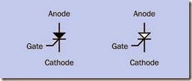
The SCR has three leads, identified as anode, cathode, and gate. Two functionally identical versions of the schematic symbol are shown in Figure 1-1. Early versions sometimes included a circle drawn around them, but this style has be- come obsolete. Care must be taken to distinguish
between the SCR symbol and the symbol that represents a programmable unijunction transistor (PUT), shown in Figure 1-2.
Figure 1-1. Two functionally identical schematic symbols for an SCR (silicon-controlled rectifier). The symbol on the left is more common.
Figure 1-2. The symbol shown here is for a programma- ble unijunction transistor (PUT). Care must be taken to distinguish it from the symbol for an SCR.
Switching Behavior
When the SCR is in its passive or nonconductive state, it will block current in either direction be- tween anode and cathode, although a very small amount of leakage typically occurs. When the SCR is activated by a positive voltage at the gate, current can now flow from anode to cathode, al- though it is still blocked from cathode to anode. When the flow reaches a level known as the latching current, the flow will continue even after the triggering voltage drops to zero. This behavior causes it to be known as a regenerative device.
If the current between anode and cathode starts to diminish while the gate voltage remains zero, the current flow will continue below the latching level until it falls below the value known as the holding current. The flow now ceases. Thus, the only way to end a flow of current that has been
initiated through an SCR is by reducing the flow or attempting to reverse it.
Note that the self-sustaining flow is a function of current rather than voltage.
Unlike a transistor, an SCR is either “on” or “off” and does not function as a current amplifier. Like a diode, it is designed to conduct current in one direction; hence the term rectifier in its full name. When it has been triggered, the impedance be- tween its anode and cathode is sufficiently low that heat dissipation can be managed even at high power levels.
The ability of SCRs to pass relatively large amounts of current makes them suitable for con- trolling the power supplied to motors and resistive heating elements. The fast switching response also enables an SCR to interrupt and abbreviate each positive phase of an AC waveform, to reduce the average power supplied. This is known as phase control.
SCRs are also used to provide overvoltage protection.
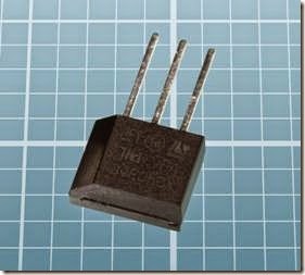
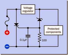
SCR packages reflect their design for a wide range of voltages and currents. Figure 1-3 shows an SCR designed for on-state current of 4A RMS (i.e., measured as the root mean square of the alternating current). Among its applications are small-engine ignition and crowbar overvoltage protection, so named because it shorts a power supply directly to ground, much like a crowbar being dropped across the terminals of a car battery (but hopefully with a less dramatic out- come). See Figure 1-15.
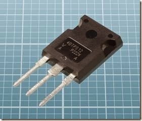
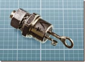
In Figure 1-4, the SCR can handle up to 800V repetitive peak off-state voltage and 55A RMS. Pos- sible applications include AC rectification, crow- bar protection, welding, and battery charging. The component in Figure 1-5 is rated for 25A and 50V repetitive peak off-state voltage. To assess the component sizes, bear in mind that the graph line spacing is 0.1”.
Figure 1-3. SCR rated for 400V repetitive off-state volt- age, no greater than 4A RMS.
Figure 1-4. SCR rated for 800V repetitive off-state volt- age, no greater than 55A RMS.
Internal Configuration
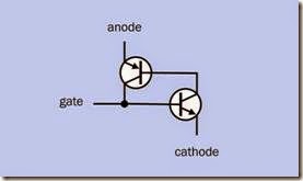
The function of an SCR can be imagined as being similar to that of a PNP transistor paired with an NPN transistor, as shown in Figure 1-6. In this simplified schematic, so long as zero voltage is applied to the “gate” wire, the lower (NPN) tran- sistor remains nonconductive. Consequently, the upper (PNP) transistor cannot sink current, and this transistor also remains nonconductive.
When voltage is applied to the “gate,” the lower transistor starts to sink current from the upper transistor. This switches it on. The two transistors now continue to conduct even if power to the “gate” is disconnected, because they have cre- ated a positive feedback loop.
Figure 1-5. Stud-packaged SCR rated for 50V repetitive off-state voltage, no greater than 25A RMS.
Figure 1-6. An SCR behaves similarly to an NPN and a PNP transistor coupled together.
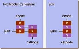
Figure 1-7 shows the same two transistors in simplified form as sandwiches of p-type and n-type silicon layers (on the left), and their combination in an SCR (on the right). Although the actual con- figuration of silicon segments is not as simple or as linear as this diagram suggests, the SCR can be described correctly as a PNPN device.
An SCR is comparable with an electromagnetic latching relay, except that it works much faster and more reliably.
Figure 1-7. The two transistors from the previous figure are shown here in simplified form as two stacks of p-type and n-type silicon layers. These layers are combined in an SCR, on the right.
Breakdown and Breakover Voltage
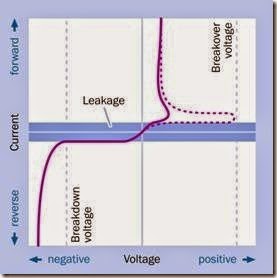
The curves in Figure 1-8 illustrate the behavior of a hypothetical SCR, and can be compared with the curves shown for a diac in Figure 2-5 and atriac in Figure 3-10. Beginning with zero voltage applied between anode and cathode, and zero current flowing (i.e., at the center origin of the graph), if we apply a voltage at the anode that is increasingly negative relative to the cathode (i.e., we attempt to force the SCR to allow negative current flow), we see a small amount of leakage, indicated by the darker blue area (which is not drawn to scale). Finally the breakdown voltage is reached, at which point the negative potential overcomes the SCR and its impedance drops rap- idly, allowing a surge of current to flow, probably damaging it.
Alternatively, starting once again from the center, if we apply a voltage at the anode that is increasingly positive relative to the cathode, two consequences are possible. The dashed curve assumes that there is zero voltage at the gate, and shows that some leakage occurs until the applied potential at the anode reaches the break- over voltage, at which point the SCR allows a large current flow, which continues even when the voltage decreases.
Figure 1-8. The solid curve shows current passing be- tween the anode and cathode of a hypothetical SCR for varying voltages, while a triggering voltage is applied to the gate. The dashed curve assumes that no triggering voltage is applied to the gate.
In practice, the SCR is intended to respond to a positive gate voltage. Under these circumstances, its behavior is shown by the solid curve in the top-right quadrant in Figure 1-8. The SCR be- gins to conduct current without having to reach the breakover voltage at the anode.
• When used as it is intended, the SCR should not reach breakdown or breakover voltage levels.
SCR Concept Demo
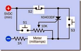
In Figure 1-9, pushbutton S1 applies voltage to the gate of the SCR, which puts the SCR in self- sustaining conductive mode. When S1 is re- leased, the meter will show that current continues to pass between the anode and the cathode. The X0403DF SCR suggested for this circuit has a holding current of 5mA, which a 5VDC supply should be able to provide with the 1K resistor in the circuit. If necessary, this resistor can be reduced to 680Ω.
Now if pushbutton S2 is pressed, the flow is interrupted. When S2 is released, the flow will not resume. Alternatively, if pushbutton S3 is pressed while the SCR is conducting current, the flow is diverted around the SCR, and when the push- button is released, the flow through the SCR will not resume. Thus, the SCR can be shut down ei- ther by a normally closed pushbutton in series with it (which will interrupt the current), or a nor- mally open pushbutton in parallel with it (which will divert the current).
Figure 1-9. In this test circuit, S1 triggers the SCR, while S2 or S3 will stop it. See text for additional details.
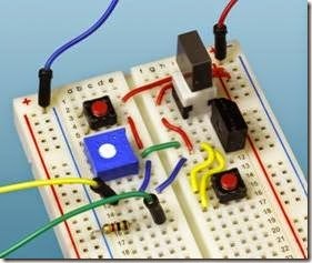
The test circuit is shown installed on a bread- board in Figure 1-10. In this photograph, the red and blue wires supply a minimum of 5VDC. The two red buttons are tactile switches, the one at top left being S1 in the schematic while the one at bottom right is S3. The large switch with a rec- tangular button is S2; this is normally closed, and opens when pressed. The X0403DF SCR is just below it and to the right. The square blue trim- mer is set to the midpoint of its range.
AC Current Applications
If the SCR is used with alternating current, it stops conducting during each negative cycle, and is retriggered in each positive cycle. This suggests one of its primary applications, as a controllable rectifier that can switch rapidly enough to limit
the amount of current that passes through it during each cycle.
Figure 1-10. A breadboarded version of the SCR test circuit. The two red buttons correspond with S1 and S3 in the schematic, while the large rectangular button at top right opens S2. See text for details.
Variants
SCRs are available in surface-mount, through- hole, and stud packages, to handle increasing currents and voltages. Some special-purpose SCRs can control currents of hundreds of amps, while high-power SCRs are used to switch thou- sands of amps at more than 10,000V in power distribution systems. They are too specialized for inclusion in this encyclopedia.
Typical power ratings for SCRs in general use are summarized in the next section.
Values
Any SCR will impose a forward voltage drop, which typically ranges from around 1V to 2V, de- pending on the component.
Because SCRs are often used to modify AC wave- forms, the current that the component can pass is usually expressed as the root mean square (RMS) of its peak value.
Commonly Used Abbreviations
• VDRM Maximum repetitive forward voltage that may be applied to the anode while no voltage is applied to the gate (i.e., when the SCR is not in conductive mode).
• VRRM Maximum repetitive reverse voltage that may be applied to the anode while no voltage is applied to the gate (i.e., when the SCR is not in conductive mode).
• VTM Maximum on-state voltage while the SCR is in conductive mode. T indicates that this value changes with temperature.
• VGM Forward maximum gate voltage.
• VGT Minimum gate voltage required to trig- ger.
• VGD Maximum gate voltage that will not trig- ger.
• IDRM Peak repetitive forward blocking cur- rent (i.e., maximum leakage).
• IRRM Peak repetitive reverse blocking current (i.e., leakage in the off state).
• IGM Maximum forward gate current.
• IT(RMS) Maximum RMS current between anode and cathode while the SCR is in con- ductive mode. T indicates that this value changes with temperature.
• IT(AV) Maximum average current between anode and cathode while the SCR is in con- ductive mode. T indicates that this value changes with temperature.
• IGT Maximum gate current required to trigger.
• IH Typical holding current.
• IL Maximum latching current.
• TC Case temperature, usually expressed as an acceptable range.
• TJ Operating junction temperature, usually expressed as an acceptable range.
Surface-mount variants may tolerate maximum anode-cathode currents that typically range from 1A to 10A. Maximum voltages as high as 500V are allowed in some cases. Leakage in the “off” state may be as high as 0.5mA or as low as 5µA. Gate trigger voltage is likely to range from 0.8V to 1.5V, and trigger current of 0.2mA to 15mA is typical.
Through-hole variants may be packaged in TO-92 format (like discrete transistors) or, more commonly, in TO-220 format (like a typical 1A voltage regulator). They may be rated for a maximum of 5A up to 50A, depending on the component, with maximum voltages ranging from 50V to 500V. Leakage is similar to surface-mount variants. The gate trigger voltage is typically around 1.5V, and trigger current ranges from 25– 50mA.
A stud-type SCR may have a maximum 50A to 500A current rating, although some components are capable of tolerating even higher values. Maximum voltages of 50V to 500V are possible. Leakage is likely to be higher than in other for- mats, with 5mA to 30mA being common. The gate trigger voltage is typically 1.5 to 3V, and trigger current may range from around 50mA to 200mA.
How to Use It
Although other applications are possible, in practice SCRs have two main applications:
• Phase control, which interrupts each positive phase of an AC power supply. It can moderate the speed of a motor or the heat generated by a resistive load.
• Overvoltage protection. This can safeguard sensitive components in a circuit where there is a DC power supply.
SCRs are often incorporated in ground-fault circuit interruptors (although not usually as dis- crete components) and in automotive ignition systems.
Phase Control
Phase control is a convenient way to control or limit the AC power delivered to a load by abbreviating each pulse in the AC waveform. This is done by adjusting the gate voltage so that the SCR blocks the first part of each positive phase, then conducts the remainder, and then stops conducting below its holding level. The SCR will then block the reversed flow in the negative phase of the AC waveform, but an additional SCR with opposite polarity can be added.
This is a form of pulse-width modulation. It is highly efficient, as the effective internal resistance of the SCR is either very high or very low, and the component does not waste significant energy in the form of heat.
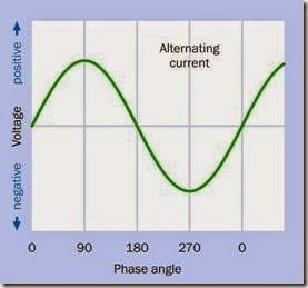
On a graph showing the fluctuating voltage of an AC waveform, a single cycle is customarily divided into four stages: (1) zero voltage, (2) maximum positive voltage, (3) zero voltage, (4) minimum negative voltage, all measurements being made between the live side of the supply and the neutral side of the supply.
The cycle then repeats. Its transitions are often referred to as phase angles of 0 degrees, 90 degrees, 180 degrees, and 270 degrees, as shown in Figure 1-11.
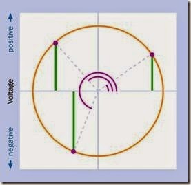
The fluctuating voltage in an AC power supply is proportional with the sine of the phase angle. This concept is illustrated in Figure 1-12. If an imaginary point (shown as a purple dot) is moving in a circular path counterclockwise at a constant speed, its vertical distance (shown in green) above or below the X axis (horizontal centerline) can represent an AC voltage corresponding with the angle (shown as purple arcs) of the circle radius to the point, each angle being measured from at the center relative to a start position at right on the X axis.
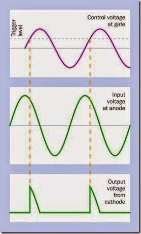
When an SCR is used for phase control, the point at which it starts to conduct may be anywhere from 0 to almost 180 degrees. This is achieved by diverting a small amount of the AC power into an RC network attached to the gate of the SCR, as shown in Figure 1-13. The capacitor in this schematic introduces a delay that can be varied by the potentiometer. This enables the SCR to be triggered even after the peak of the AC power signal. In Figure 1-14, the AC power is shown by the center (green) curve, and the slightly delayed, reduced voltage at the gate is shown by the upper, purple curve. When the gate voltage rises to the trigger level, it causes the SCR to be- gin conducting current, creating an abbreviated output shown in the bottom curve. In this way, triggering from an AC phase angle of 0 degrees to almost 180 degrees is possible. The phase angle where the SCR begins to allow conduction is known as the conduction angle.
If two SCRs with opposite polarity are placed in parallel with each other, they can be used to pro- vide phase control on both the positive-going and negative-going sections of an AC cycle. This configuration is used in high-powered devices. A triac is used for the same purpose with lower current.
Six SCRs may be used to control three-phase power.
Overvoltage Protection
The tolerance of an SCR for high current makes it suitable for use in a crowbar voltage limiting circuit.
In Figure 1-15, the SCR does not conduct current (other than a small amount of leakage) until the Zener diode senses a voltage above the maxi- mum level considered safe. The diode then al- lows power to reach the gate of the SCR. Its im- pedance drops immediately, and the resulting surge of current trips the fuse. After the cause of the overvoltage condition is corrected, the fuse can be replaced and the circuit may resume functioning.
A capacitor is included so brief spikes in the power supply will be passed to ground without triggering the SCR. A resistor of around 100Ω ensures that the gate voltage of the SCR remains near zero during normal operation. When the Zener diode starts to conduct current, the resistor acts as a voltage divider with the diode, so that sufficient voltage reaches the SCR to activate it.
This circuit may be unsuitable for low-voltage power supplies, because the Zener diode has to be chosen with a high enough rating to prevent small power fluctuations from tripping it. Bearing in mind that the real triggering voltage of the diode may be at least plus-or-minus 5% of its rated voltage, the diode may have to be chosen with at least a 6V rating in a 5V circuit, and it may not be activated until the voltage is actually 6.5V. This may be insufficient to protect the components being used with the power supply.
Figure 1-11. An AC waveform is customarily measured in degrees of phase angle.
What Can Go Wrong
Like other semiconductors, an SCR can be adversely affected by excessive heat. Usual precautions should be taken to allow sufficient ventilation and heat sinking, especially when components are moved from an open prototyping board to an enclosure in which crowding is likely.
Unexpected Triggering Caused by Heat
On a datasheet, the values for triggering current and holding current are valid only within a recommended temperature range. A buildup of heat can provoke unexpected triggering.
Unexpected Triggering Caused by Voltage
A very rapid increase in forward voltage at the anode can induce a triggering voltage in the gate by capacitive coupling. As a result, the SCR can trigger itself without any external application of gate voltage. This is sometimes known as dv/dt triggering. If necessary, a snubber circuit can be added across the anode input to prevent sudden voltage transitions.
Figure 1-12. The fluctuating voltage of an AC power sup- ply (shown as vertical green lines) is proportional with the sines of the angles (purple arcs) in this diagram. The angles are referred to as phase angles.
Confusion of AC and DC Ratings
The on-state current for an SCR is averaged only over the width of each pulse that the SCR actually conducts. It is not time-averaged over an entire AC cycle, and it will be different again from a DC rating. Care must be taken to match the current rating with the way in which the component will actually be used.
Maximum Current versus Conduction Angle
Current-carrying capability will be very significantly affected by the length of the duty cycle when the SCR is being used to abbreviate each positive AC pulse. When the SCR imposes a 120- degree conduction angle, it may be able to handle twice the average on-state current as when it is imposing a 30-degree conduction angle. The manufacturer’s datasheet should include a graphical illustration of this relationship. If an SCR is chosen for a high conduction angle, and the angle is later reduced, overheating will result, and damage is likely.
Figure 1-13. In this schematic, an SCR is used to apply phase control, adjusting the power that passes through a load.
Confusing Symbols
When reading a schematic, unfortunate errors can result from failure to distinguish between the symbol for a programmable unijunction transistor (PUT) and the symbol for an SCR. The characteristics of a PUT are described in Volume 1 of this encyclopedia.
Figure 1-14. If the AC power applied to the anode of an SCR (center) is reduced in voltage and delayed slightly by an RC network, it can trigger the SCR (top), causing it to pass only an abbreviated segment of each positive AC pulse (bottom).
Figure 1-15. In this schematic, an SCR is used to provide crowbar overvoltage protection for sensitive components.

