flip-flop
The term flip-flop is sometimes printed with a space instead of a hyphen, but the hyphenated form seems to predominate in the United States. Therefore, the hyphen is included here. The term flipflop (with neither a hyphen nor a space) is sometimes seen, but is unusual. The acronym FF is confined mostly to logic diagrams or schematics.
The term latch is sometimes used interchangeably with flip-flop but is assumed here to describe a minimal asynchronous circuit that responds immediately and transparently to an input. A flip-flop can function as a latch and also as a synchronous device which is opaque, meaning that the input does not flow directly through to the output.
What It Does
Transistors enable logic gates; logic gates enable flip-flops; and flip-flops enable many mathematical, storage, and retrieval functions in digital computing. Most flip-flops today are embedded in much larger integrated circuits that have complex functions. However, they are still available as separate components in chip form, and will be discussed on that basis here.
A flip-flop is the smallest possible unit of memory. It can store a single bit of data, represented by either a high or low logic state. (A full explanation of logic states is included in the logic gate entry. See Chapter 10.) Flip-flops are especially useful in counters, shift registers, and serial-to-parallel converters.
A flip-flop circuit can be classified as a form of bistable multivibrator, as each of its outputs is stable in one of two states until an external trig- ger stimulates it to “flip” from one state and “flop” into the other. (For a comprehensive discussion of monostable and astable multivibrators, see the timer entry in Chapter 9.)
An asynchronous flip-flop will respond immediately to a change of input, and can be used for applications such as debouncing the signal from an electromechanical switch or building a ripple counter. More often, a flip-flop is synchronous, meaning that a change in input state will be unrecognized until it is enabled by a low-to- high or high-to-low transition in a stream of pulses from an external clock.
How It Works
Every flip-flop has two outputs, each of which may have a high or low state. When the flip-flop is functioning normally, the outputs will be in opposite logical states, one being high while the other is low. These outputs are typically identified as Q and NOT-Q (the latter term meaning a letter Q with bar printed above it, sometimes referred to verbally as “Q-bar”). In datasheets and other documents where a bar symbol cannot be represented easily above a letter, the NOT-Q out- put may be represented as letter Q with an apos trophe after it, as in Q’.
Almost always, in a schematic diagram, a flip-flop is represented by a simple rectangle, with inputs and outputs identified by letters and other marks. Because a description of the inner workings is necessary before the different types of flip- flop can be understood, schematic symbols for various flip-flops will not be introduced until “Variants” on page 116.
The simplest flip-flop contains two logic gates whose function can be most easily understood if the inputs are controlled by a SPDT switch. It can be created from two NAND gates or two NOR gates, as described next. This type of component can be described as:
• asynchronous: Will accept data on an impromptu basis, as it is not synchronized with a clock.
• jam-type: Colloquial equivalent of asynchronous. The input is jammed in at any time, forcing an immediate change of output.
• transparent: The input state flows straight through to the output.
NAND-Based SR Flip-Flop
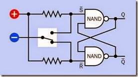
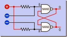
Figure 11-1 shows two NAND gates attached to a SPDT switch, with two pullup resistors. When either of the NANDs has a floating input from the switch, the pullup resistor attached to that input will maintain it in a high state. The data inputs for the NAND gates are labeled S and R, meaning Set and Reset, giving this component its name as an SR flip-flop:
• In a NAND-based SR flip-flop, a low state is considered an active logic input, as indicated by the bar placed above each letter.
• A high state is considered an inactive logic output.
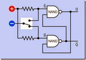
The schematic style in this figure, with diagonally crossing conductors, is universally used and easily recognizable. The equivalent schematic in Figure 11-2, which might be created by circuit- drawing software, has the same functionality but would not be immediately recognizable as a flip- flop. The “classic” crossed-conductor representation is preferable.
Figure 11-1. The schematic for a simple NAND-based SR- type flip-flop, with a switch and pullup resistors added to control two inputs.
Figure 11-2. An alternative component layout for an SR flip-flop, functionally identical to the previous schematic, but not so easily recognizable. The layout with a pair of di- agonally crossing conductors has become so ubiquitous, it should be considered to be a standard.
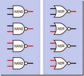
The first step toward understanding the behavior of flip-flops is to recall the relationship between the two inputs and the output of NAND or NOR gates. This is shown in Figure 11-3, where red indicates a high logic state and black indicates a low logic state.
Figure 11-3. The four possible input combinations for a NAND gate and a NOR gate, with the corresponding logical outputs. A flip-flop can be built from two NANDs or two NORs.
The behavior of a NAND gate can be summarized:
• Both inputs high: Output low.
• Other input combinations: Output high.
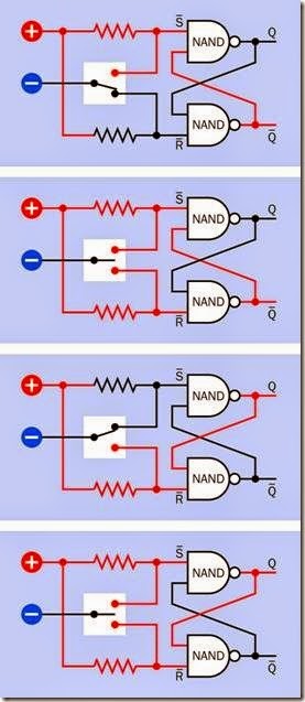
Figure 11-4 shows a series of snapshots of the SR flip-flop circuit as the switch moves from one position, through an intermediate state where it makes no connection, to the other position. Re- member that in this circuit, the active logical in- put state is low, and the active logical output state is high.
In the top panel, the pullup resistor of the lower NAND is overwhelmed by the direct connection to negative ground, which holds the R input in a low state. The other input of this gate is irrelevant, because the output from a NAND will be high if either of its inputs is low. So, the lower NAND has a high output, which feeds back to the secondary input of the upper NAND gate. The S input of this gate is high, because of the pullup resistor. Because both inputs of this gate are now high, its output is low, which feeds back to the lower gate. The lower gate doesn’t change its output, because either of its low inputs is enough to keep its output high. So, the circuit is in equilibrium. A high state on the NOT-Q output is known as the Reset state for a NAND-based flip- flop.
The second panel shows what happens if the switch now moves up into a neutral, disconnected position. The R input of the lower NAND now becomes high, because of the pullup resistor. But this NAND still has one low input, supplied by the output of the upper gate, so its output remains high, and the circuit is still in equilibrium. This is known as the Hold state for the NAND circuit.
Suppose the switch bounces to and fro between the states shown in the first two panels. The out- put from the circuit won’t change. This shows that the circuit provides a method for eliminating switch bounce—the very fast, momentary spikes that occur when the mechanical contacts of a switch open and close.
The third panel shows what happens if the switch now moves to its upper position. The top input of the upper NAND gate is now pulled low. Consequently, its output goes high. This feeds back to the lower gate. Its other input is high because of the pullup resistor. With both of its inputs high, its output goes low. The gate outputs have flip- ped and swapped values. A high state on the Q output is known as the Set state for a NAND- based flip-flop.
The circuit still remains in equilibrium even if the switch returns to its central, disconnected position shown in the bottom panel. Therefore, the debouncing capability of the circuit works equally well for both positions of the switch.
NOR-Based SR Flip-Flop
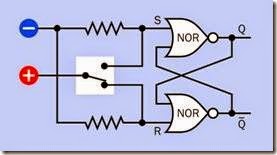
Figure 11-5 shows a similar circuit using two NOR gates attached to an SPDT switch. Because the NOR gates function differently, this circuit uses active-high input logic, and pulldown resistors are needed instead of pullup resistors. The out- put from the circuit still uses active-high logic, and is identical with the NAND-based circuit in
this respect, although the relative positions of the Q and NOT-Q outputs have been swapped.
Figure 11-4. Four snapshots of transitions in a NAND- based SR flip-flop as the switch moves down and up through an intermediate no-connection zone. See text for details.
• In a NOR-based SR flip-flop, a high state is considered an active logic input, as indicated by the absence of a bar placed above the letters S and R.
• A high state is considered an active logic output.
Figure 11-5. The schematic for a simple SR flip-flop using NOR gates instead of NANDs.
In the case of the NOR gate:
• Both inputs low: Output high.
• Other input combinations: Output low.
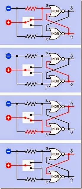
Figure 11-6 shows a series of snapshots as the switch moves from one position to the other, through intermediate states where it makes no connection. Remember that in this circuit, the active logical state is high at both the inputs and the outputs.
In this circuit, as in the previous circuit using NAND gates, it will ignore switch bounce, allowing the gate outputs to remain stable.
Forbidden States
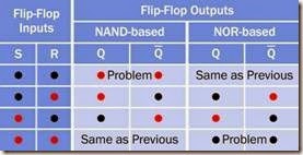
Either of the circuits described so far depicts an SR flip-flop, regardless of whether it is NAND- based or NOR-based. Its input and output states are summarized in Figure 11-7. However, as this table suggests, there are some input states that create problems.
Figure 11-6. Four snapshots of a NOR-based SR flip-flop, showing the consequence of changing switch positions, comparable with the NAND-based flip-flop.
Figure 11-7. A table of input states and the consequent output states for NAND-based and NOR-based SR flip- flops.
In either the NAND-based flip-flop or the NOR- based flip-flop, the output when the switch is in its unconnected center position will remain the same as when the switch was in its previous po- sition. This is the usefulness of the flip-flop: it re- members the previous state. These situations are identified as “Same as Previous” in the table.
The pullup resistors (in a NAND-based flip-flop) and pulldown resistors (in a NOR-based flip-flop) are intended to guarantee that both inputs will be high (NAND) or both inputs will be low (NOR) even when the switch makes no connection. Therefore, it should be impossible for both inputs to be low (NAND) or high (NOR).
But what happens if the circuit is powered up with the switch in the unconnected position? One input of each gate is controlled by the out- put of the other gate. But what will those outputs be?
In the NAND-based version, the outputs from the NANDs will be low while the chips are powering up. As soon as the NAND chips are functioning, each of them will sense that it has one input high and one input low, so it will change its output to high.
But now that each chip has a high output, it will feed back to the secondary input of the other chip. Now both chips have both inputs high. This will cause them both to change their outputs to low—but this will feed back again, flipping the outputs back to high again. In fact, if the gates
are absolutely identical, the circuit will oscillate very rapidly. This is sometimes known as ringing.
In real life, the gates will not be absolutely identical, and eventually one of them will respond fractionally ahead of the other, tipping the circuit into the state shown either in the second panel or the fourth panel in Figure 11-4. But which chip will win? There is no way of knowing. This is known as a race condition, and the winner is un- predictable.
A similar but opposite situation occurs in the NOR-based flip-flop if it is powered up with the switch in the disconnected position, and the S and R outputs are both low, because of the pull- down resistors. Here again it will be a race condition.
We can address the problem by making a rule that the switch must always be in one position or the other when the flip-flop is powered up. But what if there is a faulty switch? Or what if a power interruption occurs while the switch is changing position?
Another problem occurs if the switch makes one contact a fraction before it breaks the other con- tact. This would result in both S and R inputs being low, in a NAND flip-flop. The same state could occur if a separate logic circuit is driving the S and R inputs, and an error causes it to make S and R both low. This is shown in Figure 11-8. Because the output from a NAND gate is always high if at least one of its inputs is low, both gates now have a high output, and the circuit is stable.
The problem is, the states of the outputs from a flip-flop should always be opposite to each other. If both of them are high, this can create logic problems in the rest of the circuit attached to the flip-flop.
• In a NAND-based SR flip-flop, if S and R are both low, this is known as a forbidden state or a restricted combination.
Figure 11-8. What happens when both S and R inputs to a NAND flip-flop are low as a result of an error in a separate control circuit.
A similar problem afflicts a NOR-based SR flip- flop, except that the forbidden state will occur when the S and R inputs are both high.
• In a NOR-based SR flip-flop, if S and R are both high, this is a forbidden state or a restricted combination.
The SR flip-flop is useful as a switch debouncer, but for computing applications, it is vulnerable to errors.
The JK Flip-Flop
Because the name of the JK flip-flop shares the initials of Jack Kilby, who won a Nobel prize for his fabrication of the world’s first integrated circuit, some people speculate that this type of flip- flop was named after him. The attribution seems implausible, and may have gained currency simply because a flip-flop was the first device that Kilby happened to build when he was developing an integrated circuit.
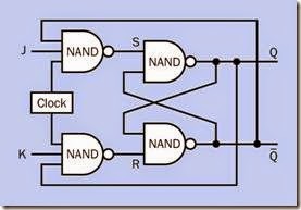
Regardless of how it came to be named, the JK design is shown in Figure 11-9. This is commonly referred to as a JK latch. The electromechanical switches that were shown driving the SR flip-flop, along with pullup or pulldown resistors, are no longer included, because the inputs at positions J and K are assumed to come from other devices that have properly defined high and low states. Their behavior may be unpredictable, but neither of them will ever have a floating state.
This is a gated circuit, meaning that an additional input stage blocks direct access to the output stage, and it is also a synchronous circuit, as it uses a train of pulses at a clock input. Two three-input NAND gates are placed in front of a NAND-based SR flip-flop, and they address the problem of simultaneous identical inputs by using crossover feedback from the second stage to the first stage (via the conductors at top and bottom of the schematic).
Figure 11-9. The basic circuit for a clocked JK flip-flop, using two additional NAND gates prepended to an SR flip- flop.
Versions of a JK flip-flop are possible using NOR gates, but are less common. Only the NAND- based version will be considered here.
In the case of a three-input NAND gate:
• All three inputs high: Output low.
• Other input combinations: Output high.
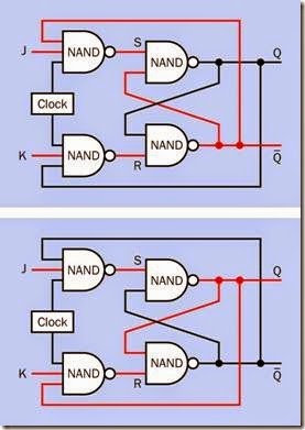
Because of the additional pair of NANDs, the circuit now recognizes a high input as logically active, instead of the low-active input in the previous SR flip-flop using NAND gates. Consequently, two simultaneous high inputs might be expected to create the type of forbidden state that was caused by two simultaneous low inputs previously. However, in Figure 11-10, the top and bot- tom panels show that simultaneous high inputs at J and K will support two possible valid outputs, where the state at Q is always opposite to the
state at NOT-Q. In fact, when both inputs are high, a positive pulse on the clock input will toggle the outputs (i.e., they will switch places). In fact, the toggling will continue so long as the clock input is high. Consequently, this type of flip-flop is in- tended for use with short clock pulses.
Figure 11-10. When the J input and the K input are both high, this no longer causes a forbidden state. The combi- nation will toggle the outputs of the flip-flop between the two states shown here.
Master-Slave Flip-Flop
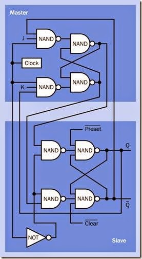
A more stable form is shown in Figure 11-11 where yet another stage has been added, this one being a “master” to the first. In fact, this con- figuration is known as a master-slave flip-flop, the slave stage being driven by the master stage but remaining inactive until a low clock input at the master stage passes through an inverter to be- come a high clock input at the slave stage. The master and slave stages thus take turns, one being activated by a high clock pulse while the other is activated by the low part of the pulse cycle. The output from the slave stage cannot feed back to the master stage while the clock pulse is still high, and thus the timing issue in the single- stage JK latch is eliminated. Because the master- slave version of the JK configuration is not trans- parent, it is correctly known as a flip-flop rather than a latch.
In addition, Preset and Clear inputs may be added to override the clock to Set or Reset the out- puts. These inputs are active-low.
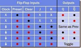
Figure 11-12 summarizes the behavior of a JK master-slave flip-flop that is triggered by the fall- ing edge of each clock pulse (shown as a downward-pointing arrow in the Clock column of the table). Note that the output will be delayed while the slave stage waits for the second part of each clock cycle.
The letter X in the table indicates that the state in that cell is irrelevant.
When J and K are both low, the states of Q and NOT-Q will remain the same as in the previous cycle, and this is still referred to as a Hold state. When J and K are both high, the outputs toggle, meaning that their new states will be opposite to the previous states.
D-T ype Flip-Flops
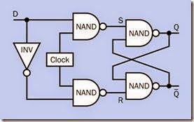
A D-type flip-flop places an inverter between two inputs to guarantee that they will always be in opposite states, and uses a clock signal to copy their states to a pair of logic gates.
When an inverter is added between the inputs in this way, either an SR flip-flop or a JK flip-flop can become a D-type flip-flop. Figure 11-13 shows the simplest possible D-type circuit, added to a basic SR flip-flop. Only one data input is now required (customarily labeled D), because it drives the other through the inverter.
Figure 11-11. A master-slave circuit that drives one flip- flop with another.
Figure 11-12. A table showing inputs and outputs for a JK master-slave flip-flop.
Figure 11-13. A simple D-type flip-flop. The inverter guarantees that the state of one input will always be opposite to the state of the other.
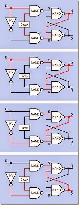
Figure 11-14 uses snapshots to show how the circuit responds to changing input and clock conditions. Initially, in the top panel, the data in- put is high, the clock input is high, and the Q output is high. In the second panel, the clock goes low, causing the output from the upper NAND gate in the input stage to change from low to high. But the upper NAND gate in the output stage still has one low input, so its state remains unchanged. In fact, the S and R inputs of the out- put NANDs are now both high, which creates the hold condition.
In the third panel, the D input changes from high to low, but this has no effect so long as the clock is low. The D input can fluctuate repeatedly, and nothing will happen until the clock goes high, as shown in the fourth panel. Now the clock copies the new D input state through to the output.
Figure 11-14. Four snapshots showing the behavior of a D-type flip-flop.
Summary
• An SR flip-flop can be used for switch de- bouncing, but in other applications it can enter an unacceptable race condition if its inputs and power supply are not carefully controlled.
• A JK flip-flop is gated, meaning that an SR circuit is preceded with an input stage and a clock input. This eliminates the race condi- tion, adds the ability to toggle the outputs, but requires a very brief clock input. The cir- cuit is edge-triggered.
• A master-slave flip-flop consists of two flip- flops, one driving the other. They can be JK type or SR type. The first flip-flop is activated by a positive clock state, while the second is activated by the subsequent negative clock state. Timing issues are resolved.
• A D-type flip-flop is gated with an inverter between the inputs, so that they cannot be simultaneously high or low. Consequently, only one input, labeled D, is needed. A high state on the D input causes a Set condition, while a low input causes a Reset condition, but only when the clock copies the status of the inputs through to the outputs. The status of the outputs remains stable (the flip-flop enters a hold condition) after the clock goes low.
• The JK circuit used to be widely used, be- cause of its versatility. The D-type circuit now predominates.
• A T-type (toggling) flip-flop exists but is un- common, and is not included in this ency- clopedia.
• Many flip-flop circuits exist in addition to the ones that have been illustrated here. Only the most commonly cited circuits have been included.
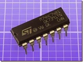
A chip containing two positive-edge triggered D-type flip-flops is shown in Figure 11-15. Each flip-flop in this component has its own data, set, and reset input and complementary outputs.
Figure 11-15. This chip contains two positive-edge triggered D-type flip-flops.
Variants
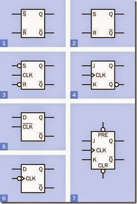
A selection of schematic symbols representing flip-flops is shown in Figure 11-16. Letters S, R, J, K, or D define the type of flip-flop. Q and NOT-Q are the outputs. CLK is the clock input but may alternatively be identified with letter E, meaning Enable. SRCK or SCLK may also identify it, the abbreviations being intended to mean “serial clock.
A triangle preceding CLK indicates that the flip- flop is positive-edge triggered. A circle, properly termed a bubble, preceding the triangle, indicates that the flip-flop is negative-edge triggered. In other locations, the bubble indicates that the input (or output) is inverted; it means the same thing as a bar printed above the text abbreviation, and indicates active-low logic. Synchronous inputs are shown on the left side of the flip-flop with the CLK input, while asynchronous inputs (if any) are shown above and below the flip-flop rectangle.
Using these guidelines, the examples in Figure 11-16 can be decoded:
1. An unclocked SR flip-flop with active-low in- puts (probably NAND-based).
2. An unclocked SR flip-flop with active-high inputs (probably NOR-based).
3. An SR flip-flop with active-high inputs, pulse-triggered by an active-high clock in- put.
4. A JK flip-flop with active-high inputs, edge- triggered by a rising-edge clock input. The bubble on the lower Q output means the same thing as a letter Q with a bar printed above it.
5. A D-type flip-flop pulse-triggered by an active-low clock input.
6. A D-type flip-flop edge-triggered by a falling-edge clock input.
7. A JK flip-flop with active-high inputs, edge- triggered by a rising-edge clock input, with asynchronous active-low Preset and Clear inputs.
Figure 11-16. The schematic symbol for a flip-flop is an annotated rectangle. See text for an explanation of the letters and marks.
Packaging
Only about 10% of the flip-flops listed by a typical parts warehouse are through-hole chips. The rest are now surface-mount. Still, even if the search is narrowed further to through-hole packages in the 74xx and 4000 series, at least 100 types still exist. They provide opportunities in education and prototyping work, even though they are less often used as standalone components.
A package often contains more than one flip- flop. Dual and quad arrays are common. The flip- flops may be independently clocked, or may share a single clock input; datasheets should be checked carefully for details. Octal flip-flops, such as the D-type 74×273, are intended for use as eight-bit registers.
Many of the older flip-flops are numbered in the 74xx series of logic chips. See Chapter 10 for a detailed guide to this numbering system and the various logic families. D-type flip-flops include 74×74, 74×75, 74×174, and 74×175, where an acronym for the logic family is substituted for the x. Old-style CMOS flip-flops include the 4042B D- type latch, the 4043B quad NOR SR flip-flop, and the 4044B quad NAND SR flip-flop. The last two are synchronous, and both allow two Set inputs, labeled S1 and S2 in the datasheet.
Examples of JK flip-flops include the 74×73, 74×76, and 74×109.
Values
As is the case with other logic chips, most flip- flops in the through-hole 74xx series are intended for 5VDC power supply while the older 4000 series may tolerate up to 18VDC. Surface-mount versions may use voltages as low as 2VDC.
See “Variants” on page 93 for a discussion of acceptable high and low logic input voltages. On the output side, the 4000 series chips are able to source less than 1mA at 5VDC, but the 74HCxx series can manage around 20mA.
If a flip-flop is used for high-speed operation, the following values must be considered:
• tS Setup time: The minimum time in nanoseconds for an input to be constant before the next clock pulse can process it.
• tH Hold time: The minimum time in nanoseconds for an input to persist after the ac- tive edge of a clock pulse that has processed it. The interaction between a clock pulse and an input state takes a brief but measurable amount of time; errors may occur if the clock is given less than that amount of time to do its job.
• tCO Clock-to-output: The elapsed time after an active clock edge, before the output changes. This is a function of the internal workings of the chip, and may be broken down into low-to-high and high-to-low out- put transitions, as follows.
• TPLH Propagation to Low-to-High: The elapsed time after an active clock edge, be- fore a low-to-high swing occurs at an output. This may not be identical to TPHL.
• TPHL Propagation to High-to-Low: The elapsed time after an active clock edge, be- fore a high-to-low swing occurs at an output. This may not be identical to TPLH.
• fMAX Maximum clock frequency for reliable operation.
• tW(H) The minimum high clock pulse width in nanoseconds.
• tW(L) The minimum low clock pulse width in nanoseconds.
In a shift register or counter, where multiple flip- flops are cascaded but they share the same clock, the tCO of one flip-flop must be shorter than the hold time of the next flip-flop, to allow the input of data to be complete before the window of op- portunity is over.
How to Use It
The asynchronous SR flip-flop is of primary use in debouncing switches. Examples are the single MAX6816, dual MAX6817, and octal MAX6818.
D- type flip-flops are widely incorporated in fre- quency dividers, which are used to count pulses and display a binary output. If the NOT-Q output is wired back to the D input, the pulse stream to the clock input will have the following effect:
1. Suppose the initial D state is low and the initial state of the NOT-Q output is low.
2. The first high clock pulse propagates the low D state into the flip-flop.
3. The next low clock state forces the NOT-Q output high. This feeds back and creates a high D input.
4. The second clock pulse propagates the high D state into the flip-flop.
5. The next low clock state pulls the NOT-Q out- put low. This feeds back and creates a low D input.
The sequence then repeats. Only one high out- put is generated at NOT-Q (or at Q) for every two clock pulses; thus the circuit can become a divide-by-two counter. If the Q output is tapped to serve as the clock input for another flip-flop, that circuit now has a divide-by-four output. A series of many flip-flops can be chained together, so long as the propagation of signals along the chain is fast enough to occur before the next clock pulse. This is known as an asynchronous counter.
For more information on the use of counters, see Chapter 13.
While flip-flops have tended to be integrated with other components in digital computing, they are still used as registers where 8 or 16 bits of serial data must be assembled at a time, prior to being disseminated as parallel data.
What Can Go Wrong
Ambiguous Documentation
For reasons which are unclear, instructional texts and tutorials can be erratic when describing flip- flops:
• A truth table may fail to clarify whether the circuit uses active-high or active-low logic.
• Truth tables from different sources are often inconsistent in their representation of cur- rent and future output states, and may even fail to include the clock status in a clocked flip-flop.
• Tutorials may include logic diagrams for some types of circuit, but not others.
• NOR gates may be used, without any men- tion that NAND gates can also be used (and may be more common or convenient).
• The active-low or active-high status of in- puts in an SR flip-flop may not be shown.
Bearing this in mind, manufacturer datasheets should be consulted whenever possible as the primary source of information.
Faulty Triggering
In many cases, a flip-flop designed for edge triggering can give erroneous results if it is level- triggered, and vice versa. Rising-edge-triggered flip-flops must be distinguished from falling- edge-triggered flip-flops. As always, it is important for similar parts that have similar functions to be stored separately.
Metastability
The behavior of flip-flops has been described in this entry under ideal conditions, where they are operating well within parameters established by the manufacturer. In reality, non-ideal scenarios may occur, especially where inputs such as data and clock, or clock and reset, are almost simultaneous. This may be difficult to avoid if a signal is received from an external source such as a sensor, with no way to control its arrival time. If the input occurs within the setup time or the hold time of a clock pulse, the flip-flop may be unable to determine whether the input precedes or follows the clock.
This may lead to metastability, meaning an un- predictable output and/or oscillations that take several clock cycles to settle into a stable state. If the output from a flip-flop may be used by two separate components with slightly different response times, one may interpret the oscillating output as a high state while the other interprets it as low. In a computing circuit, metastability can lead to calculation errors or a system crash. To avoid these issues, limits in datasheets should be observed. Attention should be paid to the man- ufacturer specifications for minimum setup time and hold time, so that the circuit has sufficient opportunity to recognize a signal and respond.
One solution to metastability is to connect multiple flip-flops in series, all sharing a common clock signal. This will tend to filter out irregularities, at the expense of requiring additional clock cycles if the flip-flops are not transparent.
Metastable-hardened flip-flops minimize meta- stability but cannot eliminate it completely.
Other Issues
Problems that tend to affect digital chips generally are listed in the section of the entry on logic gates (see “What Can Go Wrong” on page 105).

