comparator
Although a comparator has the same schematic symbol as an op-amp, their applications differ and they are described in separate sections of this encyclopedia.
This entry describes an analog comparator. A digital comparator is very different, being a logic chip that compares two binary numbers that can be referred to as A and B. Outputs from the chip indicate whether A>B or A<B or A=B. The digital comparator does not have an entry in this encyclopedia.
What It Does
A comparator is an integrated circuit chip that compares a variable voltage on one input pin with a fixed, reference voltage on a second input pin. Depending which voltage is higher, the out- put from the comparator will be high or low.
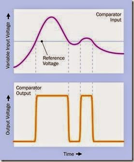
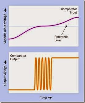
The output will make a clean transition between two fixed values, even if the input is infinitely variable. Thus the comparator can function as an analog-digital converter, as shown in Figure 6-1.
Because the output voltage range can be adjusted up or down independently of the input range, a comparator can also function as a volt- age converter.
Hysteresis
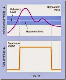
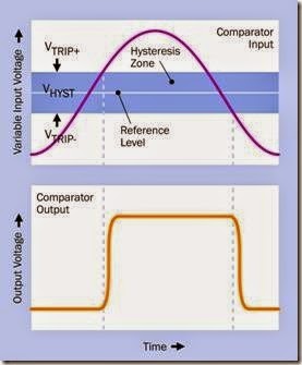
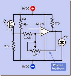
If positive feedback is added through external resistors, hysteresis can be introduced. We may imagine a hysteresis zone extending above and below the reference voltage level. Small input variations that occur within the zone will be ignored. The comparator only reacts when the in- put signal emerges above or below the hysteresis zone. When the input signal returns into the hysteresis zone, this event also will be ignored. The concept is illustrated graphically in Figure 6-2. A circuit to create hysteresis is shown in Figure 6-10.
How It Works
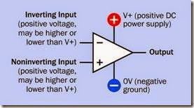
The schematic symbol for a comparator is shown in Figure 6-3. This seems identical to the symbol for an op-amp, described in Chapter 7, but an op- amp is traditionally a dual-voltage device using positive and negative power sources that are equal and opposite, in addition to a zero value midway between the two. Modern comparators mostly use a conventional single voltage, and therefore the negative symbol used in comparator schematics throughout this section of the en- cyclopedia represents 0 volts. It has the same meaning as the ground symbol found in many schematics elsewhere.
The two inputs to a comparator are described as inverting and noninverting (for reasons explained later). Confusingly, these are identified with plus and minus symbols inside the triangle that rep- resents the component. These plain black-and-
white symbols have nothing to do with the power supply.
Figure 6-1. The basic behavior of a simple comparator is shown here.
Often, in schematics, the power supply is not shown, because it is assumed to be present. However, all comparators require a power supply in order to function.
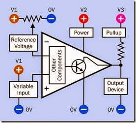
The basic internal and external connections used in conjunction with a typical comparator are shown in Figure 6-4.
The potentiometer at top left is often a trimmer, to fine-tune a reference voltage. The variable in- put can come from a sensor or any other device capable of delivering a voltage up to the limit set by V1.
The output is often an open collector from an internal bipolar transistor, as shown in the figure.
Note that as many as three different voltages can be used, as indicated by the different colors associated with V1, V2, and V3. However, they must share a common ground to enable the comparator to make valid comparisons.
When the noninverting input exceeds the volt- age of the inverting input, the output transistor goes into its “off” state, and blocks current from an external pullup resistor. Because the current from the resistor now has nowhere else to go, it is available to drive other devices attached to the comparator output, and the output appears to be high.
Figure 6-2. The performance of a comparator shown in the previous figure can be modified by the addition of hysteresis. Small variations that occur within the hysteresis zone are ignored.
When the noninverting input falls below the voltage of the inverting input, the transistor be- comes conductive, and sinks almost all the cur- rent from the pullup resistor, assuming other de- vices attached to the output have a relatively high impedance. The output from the comparator now appears to be low.
This can be summed up as follows:
• When a variable voltage is applied to the noninverting input, and it rises above the reference voltage applied to the inverting in- put, the output transistor turns off, and the comparator delivers a high output.
• When a variable voltage is applied to the noninverting input, and it falls below the ref- erence voltage applied to the inverting in- put, the output transistor turns on, and the comparator delivers a low output.
Figure 6-3. The symbol for a comparator is the same as the symbol for an op-amp, even though they often require different types of power supply and their functions are sig- nificantly different.
Figure 6-4. Connections to a comparator, and their functions.
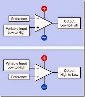
If the reference voltage and the variable voltage are swapped between the input pins, the behavior of the comparator is reversed. This relation- ship is illustrated in Figure 6-5. When a voltage transition is applied to the inverting input, the transition is inverted at the output.
Figure 6-5. Depending which input pin is used for the reference voltage, and which input carries a variable voltage, the comparator output either follows the variable voltage or inverts it.
Placement of the plus and minus signs inside the comparator symbol may vary. Most often, the minus sign is above the plus sign, as shown in all the schematics here. Sometimes, however, for convenience in drawing a schematic, the plus sign may be shown above the minus sign. Regardless of their placement, the plus sign always identifies the noninverting input, and the minus sign always identifies the inverting input. To avoid misinterpretations, schematics should be inspected carefully.
Where a power supply for the comparator is shown, the positive side is always attached to the upper edge of the symbol, while 0V ground is always attached to the lower edge.
Differences from an Op-Amp
Saturation versus linearity
The output of a comparator is optimized for saturation (high or low, without intermedi- ate levels, using positive feedback). The out- put of an op-amp is optimized for linearity (faithful reproduction of nuances in the in- put, using negative feedback).
Output mode
The majority of comparators have open- collector outputs (or open-drain outputs in CMOS devices) where the voltage is established by a pullup resistor. This can be adjusted for compatibility with other components, especially 5VDC logic. Only a minority have push-pull amplifier outputs that re- quire no pullup resistor. By comparison, among op-amps, a push-pull output that functions as a voltage source is the tradition- al default.
A comparator responds more quickly than an op-amp to changes in input voltage, if the op-amp is used in the role of a comparator. The comparator is primarily a switching de- vice, not an amplifier.
This is generally desirable in a comparator, for reasons already explained, and some components are designed with hysteresis built in. This feature is undesirable in an op- amp, as it degrades sensitivity.
Open-loop operation
(i.e., without feedback) this can be used with a comparator. An op-amp is intended for use in closed-loop circuits (i.e., with feedback), and manufacturers will not specify its per- formance in an open loop.
As previously noted, a comparator usually re- quires a single-voltage power supply, while an op-amp often requires a dual-voltage power supply.
Variants
Where a comparator uses a MOSFET output transistor, it may have an open-drain output, which requires a pullup resistor, as with an open- collector output.
Some comparators have a push-pull output, capable of supplying output current (usually a small amount). In these instances, no pullup resistor is necessary or desirable. The output volt- age range will be closest to rail-to-rail values (i.e., the range of the power supply) where MOSFETs are used for the output, as MOSFETs impose a smaller voltage drop than bipolar transistors.
The advantage of an open collector (or open drain) relative to a push-pull output is that it al- lows the output voltage to be set independently of the power supply voltage. Another advantage is that multiple outputs can be connected in parallel, as in a window comparator circuit (described below).
Some comparators incorporate a reference volt- age on the chip, based on the power supply to the chip. In this case, a separate reference voltage does not have to be supplied, and the component will draw less current.
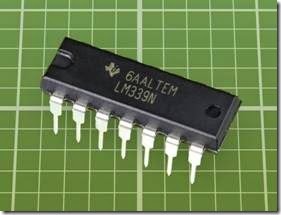
Many chips are available containing two or more comparators. This is often expressed as the number of channels in the component. A dual comparator typically allows two different voltage sources for the outputs of the comparators. They will share the same 0V ground, however. Chips such as the LM139 and LM339 contain four comparators, and are available in through-hole or surface-mount formats. They have become a generic choice, costing less than $1 apiece.
An LM339 comparator chip is shown in Figure 6-6. This is a quad chip, meaning that it contains four comparators. They share a common power supply. The chip is TTL and CMOS compatible, is typically powered by 5VDC, but can be driven by up to 36VDC. The input differ- ential voltage range also extends up to 36V.
Figure 6-6. The LM339 quad comparator chip, shown here, was introduced long ago but remains widely used.
Some comparators have an internal latch function that is accessed by a dedicated pin. The latch-enable signal forces the comparator to assess its inputs and hold an appropriate output which can then be checked by other components.
Values
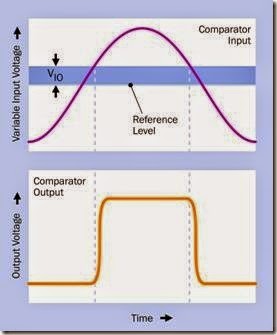
In a datasheet, VIO (also referred to as VOS) is the input offset voltage. This is a small voltage, in addition to the reference voltage, which the comparator will require to toggle its output in either direction, up or down. Figure 6-7 shows this graphically. VIO sets the limit of resolution of the comparator, which will not respond unless the input voltage exceeds the reference voltage by this amount. A smaller value for VIO is better than a larger value. Common values for VIO range from 1mV to 15mV. The actual offset voltage tends to vary between one sample of a component and another. VIO is the maximum allowed value for a component.
Because the comparator will not respond until the reference voltage is exceeded by VIO, the out- put pulse width will be narrower than if the comparator reacted at the point where the variable voltage input was precisely the same as the reference voltage.
Figure 6-7. The input offset voltage is the very small volt- age that a comparator requires, additional to the reference input voltage, before it will toggle its output from low to high or high to low.
VTRIP+ and VTRIP- are the rising and falling voltages, respectively, that will trip the comparator out- put where the comparator exhibits some innate hysteresis without an external feedback loop. They are also referred to as Lower State Transition Voltage (LSTV) and Upper State Transition Volt- age (USTV).
VHYST is the hysteresis range defined as VTRIP+ mi- nus VTRIP-. The relationship is shown graphically in Figure 6-8.
AVD is the voltage gain of a comparator, in which the letter “A” can be thought of as meaning “am- plification.” The gain is measured as a maximum ratio of output voltage to input voltage. Typically it ranges from 40 to 200.
Supply voltage for modern comparators is often low, as the components are used in surface- mount format for battery-powered devices where low power consumption is a primary concern. Thus, 3VDC is common as a power requirement, and 1.5VDC comparators are available. Still, older chips can use as much as 35VDC.
Figure 6-8. The value of VTRIP shows the hysteresis in a comparator—the range of input voltages, relative to the reference voltage, in which it will not respond.
Supply current can range from 7mA down to be- low 1µA.
ISINK is the recommended typical or maximum sink current that the component will tolerate, if it has an open-collector output. This value should be considered in relation to the power dissipation, PD.
The propagation delay in a comparator is measured from the moment when an input (usually a square wave) reaches the triggering value, to the time when the consequent output reaches 50% of its final value.
When a comparator is driving CMOS logic using a 5VDC power supply, a typical value for a pullup resistor is 100K. It does not have to be lower, be- cause CMOS has such a high input impedance.
How to Use It
In Figure 6-1, a hypothetical comparator responds immediately when the input voltage equals the reference voltage value. However, this is an idealized scenario. A magnified view, in Figure 6-9, suggests that the comparator is likely to respond with jitter when the input signal is very close to the reference voltage, because of tiny variations in heat, current, and other variables. This jitter will cause significant problems if the comparator is driving a device such as a relay, directly or indirectly.
Hysteresis eliminates this uncertainty around the transition level of the input, by telling the comparator to ignore small irregularities in the input voltage. Hysteresis is also useful in many situations where larger variations in a sensor input should be ignored. In Figure 6-2, for instance, suppose that the input voltage comes from a temperature sensor. The small bump in the right- hand section of the curve is probably unimportant; it could be caused by someone opening a door, or a person’s body heat in brief proximity to the sensor. There’s no point in responding to every little event of this type. In this application, the larger, longer-term temperature trend is what matters, and significant hysteresis is appropriate.
Also, if a comparator is being used as a thermo- stat, to switch a heating system on and off, we do not want the comparator to respond as soon as the temperature rises just a small amount. The heating system should run for a while before it elevates the temperature beyond the hysteresis zone.
The usual way to create hysteresis is with positive feedback. In Figure 6-10, a connection from the output of the comparator runs back through a 1M potentiometer to the variable (noninverting) input. The effect that this has is to reinforce the input voltage with the output voltage, as soon as the comparator input goes high. Now the input can diminish slightly without switching off the comparator. But if the input declines significant-
ly, even the feedback from the output voltage won’t be sufficient to maintain the variable input at a higher level than the reference voltage. (Re- member, the “high” output voltage from the comparator is a fixed value; it does not change in proportion with the input voltage.) Consequently, the output toggles to low. Now the variable input is deprived of help from the comparator output, so it will be low enough that it has to rise considerably to toggle the comparator back on again. During that period, once again, small variations will be ignored.
Figure 6-9. In real-world applications, tiny variations where the variable input voltage crosses the reference voltage can induce jitter in the output from a comparator that has no hysteresis.
In the schematic, a phototransistor (PT1, at left) is in series with a 3.3K resistor to adjust its voltage output to a suitable range. A 1M potentiometer at upper-left is wired as a voltage divider, so that it can establish a reference level that matches the light level that we wish to detect with the pho- totransistor.
Figure 6-10. A simple circuit to achieve hysteresis with positive feedback to the variable input of a comparator.
The 470Ω resistor is the pullup resistor, which protects the LED from excessive current. The lower 1M resistor adjusts the amount of positive feedback, which determines the width of the hysteresis zone.
Values for components may have to be adjusted depending on the supply voltage, the variable input voltage, and other factors. But the principle will remain the same. Note that in the example shown, all the positive voltage sources are identical. In practice, different voltages could be used, so long as they share a common ground.
AND gate
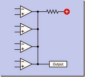
A set of open-collector comparators can function jointly as an AND gate, when their outputs are tied together with one pullup resistor. So long as all the output transistors are nonconductive, the output will be high. If just one comparator toggles into conductive mode, the output will be low. See Figure 6-11.
Figure 6-11. If the outputs of multiple open-collector comparators are tied together with a suitable pullup resistor, they will function as an AND gate.
Bistable Multivibrator
If positive feedback to the noninverting input of the comparator is sufficiently high, a voltage al- most at 0V ground will be required to counter the high output from the comparator—after which, a voltage almost equal to the supply voltage will be needed to turn it back on. In other words, the comparator is behaving like a bistable multivi- brator, or flip-flop.
Relaxation Oscillator
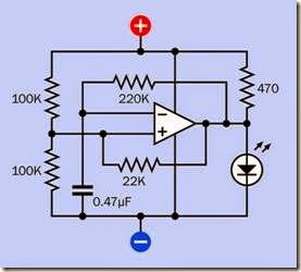
A relaxation oscillator, which is a form of astable multivibrator, can be created using direct positive feedback in combination with delayed negative feedback. In Figure 6-12, positive feedback goes to the noninverting input, as before, but negative feedback also passes through a 220K resistor to the inverting input of the comparator. A 0.47µF capacitor initially holds the inverting input low, while the capacitor charges. Gradually the ca- pacitor reaches and exceeds the charge on the noninverting input, so the output from the com- parator toggles to its low state. This means that its internal transistor is now sinking current, and it discharges the capacitor. Because the noninverting input is being held at a voltage midway between supply and ground by the two 100K re-
sistors forming a voltage divider, eventually the voltage on the inverting input controlled by the capacitor falls below the noninverting voltage, so the cycle begins again.
Figure 6-12. A comparator can be used to create a relaxation oscillator.
Level Shifter
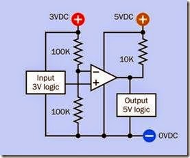
Where a comparator is used simply to change the level of an input voltage, it can be referred to as a level shifter. An example of a level shifter is shown in Figure 6-13, in which a high/low 3VDC logic input is converted to a high/low logic out- put at 5VDC.
Window Comparator
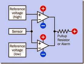
A window comparator is a circuit (not a single component) that will respond to input voltages that deviate outside an acceptable “window” of values. In other words, the circuit responds any- time the variable input is either unacceptably low or unacceptably high.
An example could be an alarm that will sound if a temperature is either too low or too high. In Figure 6-14, two comparators are used to create a window comparator circuit, both sharing a variable voltage input from a sensor. A voltage divider is necessary to establish a higher voltage limit at the noninverting input of the upper com-
parator, while a separate voltage divider would establish a lower limit at the inverting input of the lower comparator. If an alarm has an appropriate resistance, it can be used instead of a pull- up resistor. The alarm will sound when the output from either comparator is low, which happens if the inverting input has a higher voltage than the non-inverting input.
Figure 6-13. A comparator can be used to convert high
Figure 6-14. A basic, simplified circuit for a window comparator. See text for details.
A continuous converter changes its output promptly in response to a change in input. This requires continuous current consumption. Be- cause many applications only need to check the output from a comparator at intervals, power can be saved by using a clocked or latched comparator.
What Can Go Wrong
and low 3V logic inputs into high and low 5V logic outputs.
Other Applications
As previously noted, a comparator can be used as a simple analog-digital converter. It has “one bit” accuracy (i.e., its output is either high or low).
A comparator can be used as a zero point finder when its variable voltage input is attached to an AC signal. The output from the comparator will be toggled whenever the AC signal passes through zero volts. The output will be a square wave (approximately) instead of a sine wave.
Oscillating Output
The high input impedance of a comparator is vulnerable to stray electromagnetic fields. If the conductors leading to and from the comparator are relatively long, the output can couple capacitively with the input during voltage transitions, causing unwanted oscillations.
The commonly recommended solution to this problem is to add 1µF bypass capacitors to the power supply on either side of the comparator. However, some manufacturers recommend alternatives such as introducing just a small amount of hysteresis, or reducing the value of input resistors to below 10K.
If a chip contains multiple comparators, and one of them is unused, one of its input pins should be tied to the positive side of the voltage supply while the other should be tied to 0V ground, to eliminate the possibility of an oscillating output.
Confused Inputs
A comparator will function if its two inputs are swapped accidentally, but its high and low out- put states will be the inverse of what is expected. Also, if positive feedback is used, transposed in- puts can create oscillations. Because the comparator symbol may appear in a schematic with the noninverting input either below or above the inverting input, the inputs are easily transposed by accident.
One way to remember which way the inputs should be connected is to use the mnemonic: “plus, high, positive.” The plus input creates a high output when the input becomes more positive than the reference voltage on the other input. The opposite is less intuitively obvious: the mi- nus input creates a high output when the input becomes more negative than the reference volt- age on the other input.
Wrong Chip Type
Different comparators offer different outputs: open collector, open drain, and push-pull. While open collector and open drain function similarly, the pullup resistor value is likely to be different in each case. If a push-pull output is mistakenly connected as if it is open collector or open drain, it will not work correctly, if at all. Different types of comparators must be sorted and stored in clearly labeled bins.
Omitted Pullup Resistor
It is relatively easy to forget to include the pullup resistor on an open-collector output. In this case, when the transistor inside the comparator is in its nonconductive state, the output pin will be floating, with an indeterminate voltage that will create confusing or random results.
CMOS Issues
As usual when using CMOS chips, it is bad practice to allow unconnected, floating inputs. This is an issue where a chip contains multiple comparators, some of which are not being used. The solution recommended by some manufacturers is to tie one input of an unused comparator to the supply voltage, and the other input of the same comparator to ground.
Erratic Output
If positive feedback is insufficient, the comparator output may show signs of jitter. Conversely, if the positive feedback is excessive, the comparator may get stuck in an on state or an off state. Feedback must be chosen carefully.
Swapped Voltages
A comparator is often capable of controlling an output voltage that is much higher than that of its power supply. Because both voltages are ap- plied to different pins on the same chip, mistakes can be made quite easily. The chip is likely to be damaged if the voltages are swapped acciden- tally between the relevant pins.
Heat-Dependent Hysteresis Remember that the voltages at which the comparator turns on and off will vary slightly with the temperature of the component. This drift should be tested by running the comparator at higher temperatures.

