op-amp
Although a comparator has the same schematic symbol as an op-amp, their applications differ and they are described in separate sections of this encyclopedia.
The unabbreviated name for an op-amp is an operationalamplifier, but this term is seldom used.
What It Does
An op-amp is an operational amplifier consisting of multiple transistors packaged in an integrated circuit chip. It senses the fluctuating voltage difference between two inputs, uses power from an external supply to amplify that difference, and uses negative feedback to ensure that the output is an accurate replica of the input. Its amplification can be adjusted by changing the values of two external resistors.
Op-amps were developed originally using vacuum tubes, for use in analog computers, before the era of digital computing. Their implementation in integrated circuits dates from the late 1960s, when chips such as the LM741 were introduced (lower-noise versions of it still being widely used today). Multiple op-amps in a single package were introduced in the 1970s.
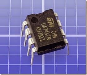
An LM741 is shown in Figure 7-1. Inside the 8-pin, DIP package is a single op-amp.
How It Works
In alternating current, voltages deviate above and below a zero value, which is sometimes referred to as the neutral value. This occurs in domestic power supplies and in audio signals, to name two very common examples. A voltage amplifier multiplies the positive and negative voltage excursions, using an external power source to achieve this. Most op-amps are voltage amplifiers.
Figure 7-1. The LM741, shown here, is still one of the most widely used op-amps.
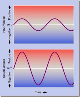
An ideal amplifier maintains a linear relationship between its input and its output, meaning that the output voltage values are a constant multiple of the input voltages over a wide range. This is illustrated in Figure 7-2, where the lower curve is a duplicate of the upper curve, the only difference being that its amplitude is multiplied by a fixed amount (usually much greater than shown here). The ratio is properly known as the gain of the amplifier, usually represented with letter A (for amplification).
Figure 7-2. In an ideal voltage amplifier, the output volt- age will be a duplicate of the fluctuating input voltage, the only difference being that the amplitude of the output is multiplied by a fixed amount. This ratio is known as the gain of the amplifier.
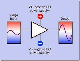
Figure 7-3 shows the triangular symbol for a generic single-input amplifier (not an op-amp). It may contain any number of components. The triangle almost always points from left to right, with its input on the left and its output on the right, and power attached above and below. This is often a dual voltage power supply, which is convenient for amplifying a signal that fluctuates above and below 0V. In some schematics, the power supply connections may not be shown, as they are assumed to exist.
Figure 7-3. The generic symbol for a single-input amplifier (not an op-amp), with the positive side of its power supply being equal and opposite in value to the negative side, and 0V being at the midpoint between them.
• While the blue negative symbol is generally used throughout this encyclopedia to indicate 0V ground, it represents a voltage identified as V− in a dual voltage power supply, being equal in value but opposite in polarity to the positive side of the supply, V+. (Some- times these voltages are indicated as V− and V+.) The output from this imaginary generic amplifier is shown in the figure as a linear amplification of the input.
Dual Inputs
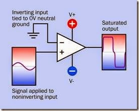
An op-amp has two inputs instead of one, and amplifies the voltage difference between them. Its symbol is shown in Figure 7-4. The upper input in this figure is held at 0V, midway between V+ and V−. Because the op-amp has so much gain, an accurate reproduction of its input would cre- ate an output exceeding the voltage of the power supply. Because this is not possible, the output tends to become saturated and consequently is clipped when it reaches its maximum value, as shown in the figure. The thumbnail graphs give only an approximate impression, as they are not drawn to the same scale.
Figure 7-4. An op-amp has so much gain, its output will tend to saturate, producing a square wave regardless of the shape of the input.
The small black plus and minus signs alongside the two inputs to the op-amp have nothing to do with the voltage supplied to the component. The “minus” input is properly referred to as the inverting input while the “plus” input is the noninverting input, in recognition of their functions.
The inputs are sometimes arranged with the mi- nus above the plus, and sometimes with the plus above the minus. Schematics should be inspected carefully to note which arrangement is being used.
The positive and negative power connections to the op-amp may be omitted, but if shown, they always place V+ at the top, regardless of which way around the inputs are presented.
If a signal is applied to the noninverting input, while the inverting input is held at 0V ground, the op-amp provides an output in which the voltage is not inverted relative to the input.
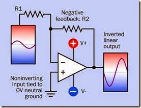
If the input connections are swapped, so that the inverting input receives the incoming signal while the noninverting input is tied to 0V ground, the output from the op-amp is inverted (the gain remains the same). See Figure 7-5.
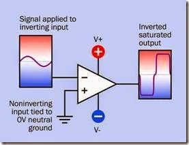 Figure 7-5. When the incoming signal is applied to the in- verting input of an op-amp while its noninverting input is held at 0V ground, the output is inverted.
• An op-amp that is being used without any other components to moderate its output is functioning in open loop mode.
Negative Feedback
To create an output that is an accurate replica of the input, the op-amp must be brought under control with negative feedback to the input sig- nal. This is illustrated in Figure 7-6. A resistor connects the output back to the inverting input, so that the input is automatically reduced to the point where the output is no longer saturated. The values of R1 and R2 will determine the gain of the op-amp, as explained in “How to Use It” on page 53. The op-amp is now functioning in its in- tended closed loop mode, meaning that the out- put is being tapped for feedback.
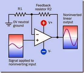
To obtain a linear output that is noninverted, connections are made as shown in Figure 7-7. The resistors form a voltage divider between the output and 0V ground, effectively increasing the comparison value on the inverting input.
Figure 7-6. A resistor applies negative feedback to the in- verting input of an op-amp, and creates a linear output.
Figure 7-7. Where the incoming signal is applied to the noninverting input, negative feedback is created by using a pair of resistors forming a voltage divider between the output and 0V ground.
• Note that the gain of an op-amp is specific to a particular frequency range of AC signal. This is discussed in “How to Use It” on page 53.
Op-Amps and Comparators
A comparator can be regarded as a type of op- amp, and in fact an op-amp can be used as a comparator, comparing a variable DC voltage on one input with a reference voltage on another input. However, the two types of components have diverged in design to the point where they should be considered separately. The distinction is sufficiently important to have prompted Texas Instruments to issue an Application Report in 2001 titled “Op Amp and Comparators—Don’t Confuse Them!”.
Differences in function are summarized in the previous entry discussing comparators (see “Dif- ferences from an Op-Amp” on page 42).
Variants
Because op-amps are mostly low-current devices, they are widely available in very small surface-mount formats, in addition to the through-hole DIP packages which used to be more common.
Many chips are available containing two or more op-amps. This is often expressed as the number of channels in the component. A dual chip contains two op-amps, while a quad chip contains four op-amps. Usually all the op-amps in a chip share the same power supply. Bipolar or CMOS transistors may be used.
Because op-amps are widely available in dual and quad packages, it’s quite common for a circuit designer to have one op-amp in a chip “left over.” The designer may be tempted to use that spare unit as a comparator instead of installing an additional chip. To address this situation, some manufacturers offer hybrid op-amp chips containing an additional comparator. The Texas Instruments TLV2303 and TLV2304 are examples.
Values
The op-amps derived from 1970s designs often tolerate a wide range of power-supply voltages. Plus-or-minus 5VDC to plus-or-minus 15VDC is a common range. Modern op-amps are available that run from as little as 1VDC to as much as 1,000VDC.
Op-amps are available for frequencies ranging from 5KHz all the way up to 1GHz.
A “classic” op-amp such as the LM741, which is still widely used, will operate with a power supply ranging from plus-or-minus 5VDC to plus-or- minus 22VDC. Its output is rated for up to 25mA, and its input impedance is at least 2MΩ. The most current it will draw from an input is around 0.5µA.
VIO is the input offset voltage. In an ideal compo- understanding of the complexities of mathematics describing alternating current, which are not included this encyclopedia. Almost all the appli- cations have a common starting point, however, which is to establish and control the gain of the feedback circuit.
Controlling the Gain
nent, the output from an op-amp should be 0V
when its inputs have a voltage difference of 0V.
"AVOL
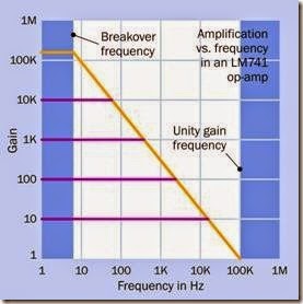
is the open-loop voltage gain, defined as the
In practice, the output will be 0V when the inputs differ by the offset voltage. VIO is likely to be no greater than a couple of mV, and negative feed- back can compensate for the offset.
VICR is the common mode voltage range. This is the range of input voltages that the op-amp will tolerate. This can never be more than the positive power supply voltage and will often be less, de- pending on the types of transistors that are used on the input side. If an input voltage goes outside the common mode voltage range, the op-amp will stop functioning.
VIDR is the input differential voltage range—the maximum permissible difference between peak positive and peak negative input voltages. This is often expressed as plus-or-minus the power supply voltage, or slightly less. Exceeding the range can have destructive consequences.
IB is the input bias current, averaged over the two inputs. Most op-amps have extremely high input impedance and consequently use very low input currents.
Slew rate at unity gain is the rate of change of the output voltage caused by an instantaneous change on the input side, when the output of the op-amp is connected directly back to the inverting input (during operation in noninverting mode).
How to Use It
In addition to being an amplifier for AC signals, an op-amp can serve as an oscillator, filter, signal conditioner, actuator driver, current source, and voltage source. Many applications require some
maximum voltage amplification that can be
achieved when no feedback is applied from the output to an input. This remains constant until the AC frequency rises to a point known as the breakover frequency. If the frequency continues to rise, the maximum gain diminishes quite rap- idly, until finally it terminates in 1:1 amplification at the unity gain frequency. This transition is shown by the orange line in Figure 7-8. The length of each purple line shows the frequencies which can be tolerated when the op-amp is used in closed-loop mode, and a negative feedback loop limits the gain. For example, where the gain is just 10:1, it can remain constant to just above 10KHz.
Note that both of the scales in this graph are log- arithmic.
Calculating Amplification
So long as an op-amp is used within the bound- aries of the graph, its voltage amplification can be controlled by choosing appropriate feedback and input resistors. If the op-amp is being used in noninverting mode, and R1 and R2 are placed as shown in Figure 7-7, the amplification ratio, A, is found approximately by the formula:
A = (approximately) 1 + (R2 / R1)
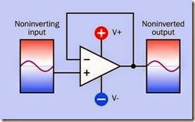
From this it can be seen that when R1 is very large compared with R2, the gain diminishes to near unity. If R1 becomes infinite and R2 is zero, the gain is exactly 1:1. This can be achieved by re- placing R2 with a section of wire (theoretically of zero resistance) and omitting R1 entirely, as in Figure 7-9. In this configuration, the output from the op-amp should be identical with its input.
Figure 7-8. Where each horizontal purple line meets the diagonal orange line, this is the maximum frequency that can be used without reduction in the maximum gain of an op-amp.
Figure 7-9. While an op-amp is in noninverting mode, if the feedback resistor is replaced with a section of wire and the 0V ground connection is omitted entirely, the gain of the op-amp diminishes theoretically to 1:1.
If the op-amp is being used in inverting mode, and R1 and R2 are placed as shown in Figure 7-6, then the voltage amplification ratio, A, is found approximately by the formula:
A = (approximately) −(R2 / R1)
• Note the minus sign. In inverting mode, gain is expressed as a negative number.
• In a practical circuit, at the expected fre- quency, the amplification factor established by choice of resistors should be no more than 20.
• An inverting circuit has a relatively low input impedance. For this reason, in most applica- tions, a noninverting circuit is preferred.
Unintentional DC Voltage Amplification
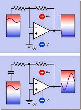
Although the op-amp is intended primarily as an AC signal voltage amplifier, it will also amplify a DC difference between the voltages on its inputs. In the upper section of Figure 7-10, a positive DC offset is inverted and amplified to the point where the output is forced to its negative limit, and the signal is lost, because its fluctuations have been overwhelmed by the positive offset. A coupling capacitor (shown in the lower section of the figure) removes the DC voltage while pass- ing the AC signal. The appropriate capacitor val- ue will depend on the frequency of the signal.
Low-Pass Filter
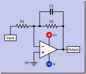
An op-amp can facilitate a very simple low-pass audio filter, just by adding a capacitor to the basic inverting circuit previously shown in Figure 7-6. The filter schematic is shown in Figure 7-11. Capacitor C1 is chosen with a value that passes higher audio frequencies and blocks lower audio frequencies. Because the gain of the basic invert- ing circuit is approximately −(R2 / R1), the op- amp functions normally when the impedance of C1 is blocking the low frequencies, forcing them to pass through R2. Higher frequencies, however, are able to bypass R2 through C1, lowering the effective resistance of the feedback section of the circuit, thus reducing its gain. This way, the power of the op-amp is greatly reduced for higher frequencies compared with lower frequencies. A passive RC circuit could achieve the same effect, but would attenuate the signal, while the op- amp circuit boosts part of it.
Figure 7-10. The addition of a capacitor at the input of an op-amp is often necessary to prevent any DC voltage off- set being amplified. In the upper section of this figure, a DC offset is large enough to force the inverted output to its negative limit, and the signal is completely lost.
Figure 7-11. A very basic low-pass filter, which works by allowing capacitor C1 to bypass resistor R2 at higher au- dio frequencies.
High-Pass Filter
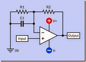
A simple high-pass filter can be created by adding a capacitor to the basic noninverting circuit previously shown in Figure 7-7. The filter schematic is shown in Figure 7-12. Once again capacitor C1 is chosen with a value that passes higher audio frequencies and blocks lower audio frequencies. Because the gain of the basic non- inverting circuit is approximately 1 + (R2 / R1), the op-amp functions normally when the impedance of C1 is blocking the low frequencies, forcing them to pass through R1. Higher frequencies, however, are able to bypass R1 through C1, lowering the effective resistance of that section of the circuit, thus reducing the negative feedback and increasing the gain. This way, the power of the op-amp is increased for higher frequencies compared with lower frequencies. A passive RC circuit could achieve the same effect, but would attenuate the signal, while the op-amp circuit boosts part of it.
Figure 7-12. A very basic high-pass filter, which works by allowing capacitor C1 to bypass resistor R1 at higher audio frequencies.
Relaxation Oscillator
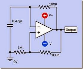
The schematic in Figure 7-13 is similar to the circuit shown in Figure 6-12 using a comparator. It functions as a relaxation oscillator, which is a form of astable multivibrator. The lower half of the circuit is a positive feedback loop that reinforces the output while the upper half of the circuit is charging the capacitor. Eventually the charge on the capacitor exceeds the voltage on the noninverting input of the op-amp, creating negative feed- back that exceeds the positive feedback. The capacitor discharges and the cycle repeats. The component values in the figure should generate an output that runs at around 2Hz. Reducing the value of the capacitor will increase the frequency.
Single Power Source
A few op-amps are designed to work from single voltages, but they are a relatively small minority, and will clip the output signal if the input goes negative. Power supplies are readily available that provide multiple voltages such as +15VDC, 0V, and -15VDC. They are ideal for driving an op- amp—but may not be useful for any other com- ponents in the circuit. Can an op-amp that is de- signed for dual voltages be made to run from a single supply, such as 30VDC?
Figure 7-13. A relaxation oscillator.
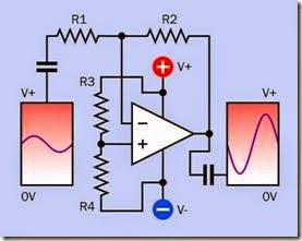
This is relatively easy to do. The op-amp simply needs a potential difference to power its internal transistors, and 30VDC on the V+ pin with 0VDC on the V− pin will work just as well as +15VDC and -15VDC. However, referring back to Figure 7-6, if the op-amp is used in inverting mode, an intermediate voltage must be supplied to the noninverting input. Likewise, in noninverting mode, an intermediate voltage is necessary for one of the inputs, and must be half-way
between the extremes of the power supply. If the supply is +15VDC and -15VDC, the midpoint is 0V. If the supply is 30VDC and 0V, the midpoint is 15VDC.
Because the inputs of an op-amp have a very high impedance and draw negligible current, the intermediate voltage can be provided with a simple voltage divider, as shown in Figure 7-14, where R3 and R4 should be no greater than 100K each. Their exact values are not important, so long as they are equal.
Figure 7-14. A voltage divider, comprised of R3 and R4 in this schematic, can provide a voltage halfway between V+ and negative ground, enabling the op-amp to use just one power supply instead of two.
A coupling capacitor should still be used on the input side, as shown, because there is no guarantee that the input signal will be centered precisely on 15V, and any offset will be amplified, potentially causing clipping of the signal. For similar reasons, a coupling capacitor is also added on the output side.
Offset Null Adjustment
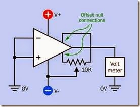
Some op-amps provide two pins for offset null adjustment, which is a setup process to ensure that identical voltage on the two inputs will pro- duce a null output. This is a way of compensating for any internal inconsistencies introduced during the manufacturing process.
To perform offset null adjustment, both input pins are connected directly to 0V ground, and the ends of a trimmer potentiometer (typically, 10K) are connected with the offset null pins, while the wiper of the potentiometer is centered and then connected with the negative power supply. The probes of a meter that is set to measure DC volts are placed between the output of the op-amp and 0V ground. The potentiometer is then ad- justed until the meter shows a reading of 0VDC. A schematic is shown in Figure 7-15.
Figure 7-15. Connections for making an offset null adjust- ment to an op-amp that allows this procedure.
What Can Go Wrong
Power Supply Problems
Op-amps are especially vulnerable to reversed polarity in a power supply. If there is even a re- mote possibility of this occurring, a diode in series with one side of the supply can provide pro- tection.
A more realistic concern is the destructive con- sequence of an input signal that exceeds the power supply voltage(s) of the op-amp. Even if the input is within the acceptable range, it can still cause permanent damage if it is applied be- fore the op-amp powers up.
Bad Connection of Unused Sections
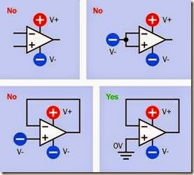
Multiple op-amps are often combined in a single package. If some of these “sections” remain un- used, they will still receive power from the shared supply, and will attempt to function. If the inputs are left unconnected, they will pick up small stray voltages by capacitance or induction, and in the absence of negative feedback, the op-amp will create unpredictable outputs, consuming power and possibly interacting with other sections of the same chip. Figure 7-16 shows three incorrect options for addressing this problem, and one recommended option (derived from Texas In- struments Application Report SLOA067).
Figure 7-16. When multiple op-amps share a chip, one that is unused will still receive power from the shared sup- ply. Its inputs must not be allowed to float, and must be connected to minimize activity and power consumption. Three common errors are shown here, with one recommended option. Note the distinction between 0V ground (0V) and negative power (V−).
Oscillating Output
The inputs of an op-amp are vulnerable to stray electromagnetic fields. If the conductors leading to and from the op-amp are relatively long, the output can couple capacitively with the input during voltage transitions, causing unwanted oscillations.
The commonly recommended solution to this problem is to add a 1µF bypass capacitor be- tween the power supply and 0V ground. How- ever, some manufacturers recommend alternatives such as introducing a very small amount of hysteresis, or reducing the value of input resistors to below 10K.
Confused Inputs
A schematic may show an op-amp with the non- inverting input above the inverting input, or vice versa. The only indication of this will be the plus and minus signs inside the chip, which can be extremely small and easily overlooked. For convenience in drawing a diagram, two op-amps in the same circuit may have their inputs shown in opposite configurations. Special care must be taken to verify that the inverting and noninverting input pins on a chip are correctly assigned.

