REPAIR OF PRINTED CIRCUIT BOARDS AND CARDS
Removal and replacement of components on boards and circuit cards are, by far, the most common types of repair. Equally important is the repair of damaged or broken cards. Proper repair of damaged boards not only maintains reliability of the board but also maintains reliability of the system.
Cards and boards may be damaged in any of several ways and by a number of causes. Untrained personnel making improper repairs and technicians using improper tools are two major causes of damage. Improper shipping, packaging, storage, and use are also common sources of damage. The source of damage most familiar to technicians is operational failure. Operational failures include cracking caused by heat, warping, component overheating, and faulty wiring.
Before attempting board repairs, the technician should thoroughly inspect the damage. The decision to repair or discard the piece depends on the extent of damage, the level of maintenance authorized, operational requirements, and the availability of repair parts and materials. The following procedures will help you become familiar with the steps necessary to repair particular types of damage. Remember, only qualified personnel are authorized to attempt these repairs.
Repair of Conductor and Termination Pads
Conductor (run) and pad damage is very common. The technician must examine the board for nicks, tears, or scratches that have not broken the circuit, as well as for complete breaks, as shown in figure 3-
23. Crack damage may exist as nicks or scratches in the conductor. These nicks or scratches must be
repaired if over one-tenth of the cross-sectional area of the conductor is affected as current-carrying capability is reduced. Cracks may also penetrate the conductor.
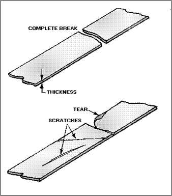 Figure 3-23.—Pcb conductor damage.
CRACK REPAIR.—Four techniques are used to repair cracks in printed circuit conductors. One method is to flow solder across the crack to form a solder bridge. This is not a high-reliability repair since the solder in the break will crack easily.
The second method is to lap-solder a piece of wire across the crack. This method produces a stronger bond than a solder bridge; but it is not highly reliable, as the solder may crack.
A third repair technique is to drill a hole through the board where the crack is located and then to install an eyelet in the hole and solder it into place.
The fourth method is to use the clinched-staple method, shown in figure 3-24. It is the most reliable method and is recommended in nearly all cases.
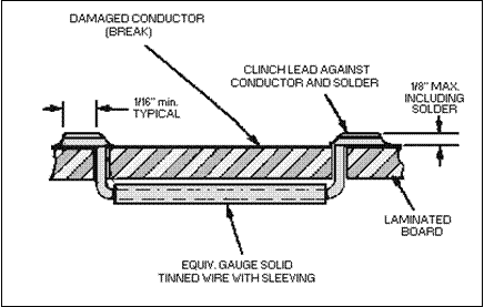 Figure 3-24.—Clinched-staple repair of broken conductor.
Pads or conductor runs may be completely missing from the board. These missing pads or runs must be replaced. Also included in this type of damage are conductors that are present but damaged beyond repair.
REPLACING DAMAGED OR MISSING CONDUCTORS.—The procedures used to replace damaged or missing conductors are essentially the same as using the clinched-staple method of conductor repair.
REPLACING THE TERMINATION PAD.—Many times the termination pad, as well as part of the conductor, is missing on the board. In these cases, a replacement pad is obtained from a scrap circuit board. Refer to figure 3-25 as you study each step.
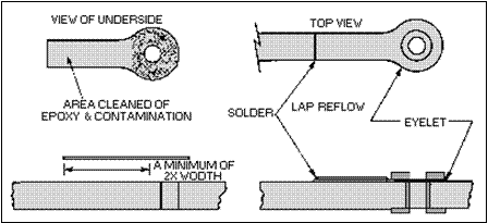 Figure 3-25.—Replacement of damaged termination pad.
The underside of the replacement pad and the area where it will be installed is cleaned. An epoxy is used to fasten the replacement pad to the board. An eyelet is installed to reinforce the pad before the epoxy sets and cures. This ensures a good mechanical bond between the board and pad and provides good electrical contact for components. After the epoxy cures, the new pad is lap-soldered to the original run.
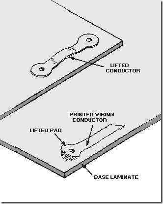
REPAIRING DELAMINATED CONDUCTORS.—DELAMINATED CONDUCTORS (figure 3-
26) are classified as conductors no longer bonded to the board surface. Separation of the laminations may occur only on a part of the conductor. Proper epoxying techniques ensure complete bonding of the
conductor to the circuit board laminate. The following procedures are used to obtain a proper bond:
Figure 3-26.—Delaminated conductors.
1. A small amount of epoxy is mixed and applied to the conductor and the conductor path; no areas are left uncoated.
2. The conductor is clamped firmly against the board surface until the epoxy has completely cured.
REPLACING EYELETS.—Eyelets have been referred to in several places in this topic. Not only are they used for through-the-board terminations, but also to reinforce some types of board repairs. As with any kind of material, eyelets are subject to damage. Eyelets may break, they may be installed improperly, or they may be missing from the equipment. When an eyelet is missing or damaged, regardless of the kind of damage, it should be replaced. The guidelines for the selection and installation of new eyelets are far too complex to explain here. However, they do comprise a large part of the 2M technician’s training.
Repair of Cracked Boards
When boards are cracked, the length and depth of the cracks must be determined. Also, the disruption to conductors and components caused by cracks must be determined by visual inspection. To avoid causing additional damage, the technician must exercise care when examining cracked boards and
must not flex the board. Rebuilding techniques must be used to repair damage, such as cracks, breaks, and holes that extend through the board. The following steps are used to repair cracks:
1. Abrasive methods are used to remove all chips and fractured material.
2. The edges of the removed area are beveled and undercut to provide bond strength.
3. A smoothly surfaced, nonporous object is fastened tightly against one side of the removed area.
4. The cutaway area is filled with a compound of epoxy and powdered fiberglass (figure 3-27).
Extreme care is exercised to prevent the formation of voids or air bubbles in the mixture.
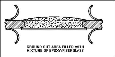 Figure 3-27.—Repair of cracked pcbs.
5. The surface of the filled area is smoothed to make it level with the surface of the original board.
6. The board is cured, smoothed, redrilled, and cleaned.
Broken Board Repair
Broken boards should be examined to determine if all parts of the board are present and if circuit conductors or components are affected by the break. They are also examined to determine if the broken pieces may be rejoined reliably or if new pieces must be manufactured.
Breaks and holes are repaired in the same manner as cracks unless broken pieces are missing or the hole exceeds 1/2 inch in diameter. In such cases, the following repair steps are used:
1. The same technique used in repairing cracks is used to prepare the damaged edge.
2. A piece as close in size to the missing area as possible is cut from a scrap board of the same type and thickness. The edges of this piece are prepared in the same manner as the edges of the hole.
3. A smooth-surfaced object is tightly fastened over one side of the repair area, and the board is firmly clamped in an immovable position with the uncovered area facing up.
4. The replacement piece is positioned as nearly as possible to the original board configuration and firmly clamped into place.
5. The repair is completed using the same epoxy-fiberglass mixture and repair techniques used in the patching repair method discussed in the following section on burned board repair.
Burned Board Repair
Scorched, charred, or deeply burned boards should be inspected to determine the size of the discolored area and to identify melted or blackened conductors and burned, melted, or blackened components. The depth of the damage, which may range from a slight surface discoloration to a hole burned through the circuit board, should also be determined. Damage not extending through the board may be repaired by patching (figure 3-28). The following procedure is used in the repair of these boards.
 Figure 3-28.—Repair of surface damage.
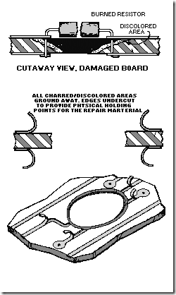
1. If the board is scorched, charred, or burned, all discolored board material is removed by abrasive methods, as shown in figure 3-29. Several components in the affected area may have to be desoldered and removed before the repair is continued.
Figure 3-29.—Repair of burned boards.
2. Repairable delaminations not extending to the edge of the circuit board should be cut away by abrasive methods until no delaminated material remains.
3. Delaminated material is not removed if it is repairable.
4. After all damaged board material is removed, the edge of the removed area is beveled and undercut to provide holding points for the repair material.
5. Solvent is used to clean thoroughly and to remove all loose particles.
6. A compound of epoxy and powdered fiberglass is mixed and used to fill the cutaway area.
7. The epoxy repair mixture is cured according to the manufacturer’s instructions.
8. The surface of the filled area is leveled after the compound is cured.
9. If delaminations extend to the edge of the board, the delaminated layers are filled completely with the repair mixture and clamped firmly together between two flat surfaces.
10. After the cure is completed, abrasive methods are used to smooth the repaired surface to the same level as the original board.
11. If necessary, needed holes are redrilled in the damaged area, runs are replaced, eyelets and components are installed, and the area is cleaned. Figure 3-30 shows the repaired area ready for components.
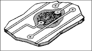 Figure 3-30.—Repaired board ready for components.
Q29. List three causes of damage to printed circuit boards.
Q30. What is the preferred method of repairing cracked runs on boards?
Q31. Damaged or missing termination pads are replaced using what procedure? Q32. How is board damage caused by technicians?
Q33. What combination of materials is used to patch or build up damaged areas of boards?

