INSTALLATION AND SOLDERING OF PRINTED CIRCUIT COMPONENTS
The 2M technician should restore the electronic assembly at least to the original manufacturer’s standards. Parts should always be remounted or reassembled in the same position and with termination methods used by the original manufacturer. This approach ensures a continuation of the original reliability of the system.
High reliability connections require thoroughly cleaned surfaces, proper component lead formation and termination, and appropriate placement of components on the board. The following paragraphs describe the procedures for properly installing components on a board including the soldering of these components.
Termination Area Preparation
The termination areas on the board and the component leads are thoroughly cleaned to remove oxide, old solder, and other contaminants. Old or excess solder is removed by one of the desoldering techniques explained earlier in this topic. A fine abrasive, such as an oil-free typewriter eraser, is used to remove oxides. This is not necessary if the area has just been desoldered. All areas to be soldered are cleaned with a solvent and then dried with a lint-free tissue to remove cleaning residue.
Component Lead Preparation
Component leads are formed before installation. Both machine- and hand-forming methods are used to form the leads. Improper lead formation causes many repairs to be unacceptable. Damage to the SEALS (point where lead enters the body of the component) occurs easily during the forming process and results in component failure. Consequently, lead-forming procedures have been established. To control the lead-forming operation and ensure conformity and quality of repairs, the technician should ensure the following:
1. The component is centered between the holes, and component leads are formed with proper bend-radii and body seal-to-bend distance.
2. The possibility of straining component body seals during lead forming is eliminated.
3. Stress relief loops are formed without straining component seals while at the same time providing the desired lead-to-lead distances.
4. Leads are measured and formed for both horizontal and vertical component mounting.
5. Transistor leads are formed to suit standard hole spacing.
Lead-Forming Specifications.
Component leads are formed to provide proper lead spacing.
-
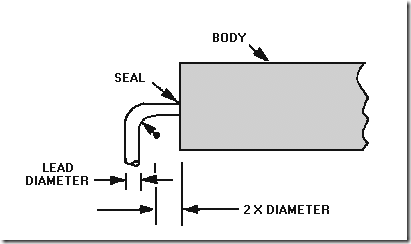
· The minimum distance between the seal (where the lead enters the body of the component) and the start of the lead bend must be no less than twice the diameter of the lead, as shown in figure 3-13.
Figure 3-13.—Minimum distance lead bend to component body.
-
· Leads must be approximately 90 degrees from their major axis to ensure free movement in hole terminations, as shown in figure 3-14.
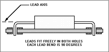 Figure 3-14.—Ideal lead formation.
-
· In lead-forming, the lead must not be damaged by nicking.
-
· Energy from the bending action must not be transmitted into the component body.
COMPONENT PLACEMENT.—Where possible, parts are remounted or reassembled as they were in the original manufacturing process. To aid recognition, manufacturers use a coding system of colored dots, bands, letters, numbers, and signs. Replacement components are mounted to make all identification markings readable without disturbing the component. When components are mounted like the original, all the identification markings are readable from a single point.
Component identification reads uniformly from left to right, top to bottom, unless polarity requirements determine otherwise, as shown in figure 3-15. To locate the top, position the board so the part number may be read like a page in a book. By definition, the top of the board is the edge above the part number.
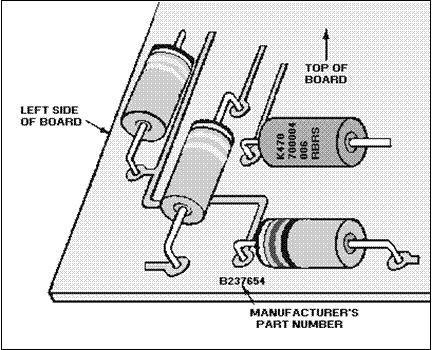 Figure 3-15.—Component arrangement.
When possible, component identification markings should be visible after installation. If you must choose between identification and electrical value markings, the priority of selection is as follows: (1) electrical value, (2) reliability level, and (3) part number.
Components are normally mounted parallel to and on the side opposite the printed circuitry and in contact with the board.
FORMATION OF PROPER LEAD TERMINATION.—After component leads are formed and inserted into the board, the proper lead length and termination are made before the lead is soldered. Generally, if the original manufacturer clinched (either full or semi) the component leads, the replacement part is reinstalled with clinched leads.
When clinching is required, leads on single- and double-sided boards are securely clinched in the direction of the printed wiring connected to the pad. Clinching is performed with tools that prevent damage to the pad or printed wiring. The lead is clinched in the direction of the conductor by bending the lead. The leads are clipped so that their minimum clinched length is equal to the radius of the pad. Under no circumstances does the clinched lead extend beyond the pad diameter. Natural springback away from the pad or printed wiring is acceptable. A gap between the lead end and the pad or printed wiring is acceptable when further clinching endangers the pad or printed wiring. These guidelines ensure uniform lead length.
Q14. To what standards should a technician restore electronic assemblies? Q15. How is oxide removed from pads and component leads?
Q16. Leads are formed approximately how many degrees from their major axis?
Q17. When you replace components, identification marks must meet what requirements?
Q18. In what direction are component leads clinched on single- and double-sided boards?
Soldering of PCB Components
The fundamental principles of solder application must be understood and observed to ensure consistent and satisfactory results. As discussed in topic 2, the soldering process involves a metal-solvent action that joins two metals by dissolving a small amount of the metals at their point of contact.
SOLDERABILITY.—As the solder interacts with the base metals, a good metallurgical bond is obtained and metallic continuity is established. This continuity is good for electrical and heat conductivity as well as for strength. Solderability measures the ease with which molten solder wets the surfaces of the metals being joined. WETTING means the molten solder leaves a continuous permanent film on the metal surface. Wetting can only be done properly on a clean surface. All dirt and grease must be removed and no oxide layer must exist on the metal surface. Using abrasives and/or flux to remove these contaminants produces highly solderable surfaces.
HEAT SOURCE.—The soldering process requires sufficient heat to produce alloy- or metal-solvent action. Heat sources include CONDUCTIVE, RESISTIVE, CONVECTIVE, and RADIANT types. The type of heat source most commonly used is the conductive-type soldering iron. Delicate electronic assemblies require that the thermal characteristics of a soldering iron be carefully balanced and that the iron and tip be properly matched to the job. Successful soldering depends on the combination of the iron tip temperature, the capacity of the iron to sustain temperature, the time of iron contact with the joint, and the relative mass and heat transfer characteristics of the object being soldered.
SELECTION OF PROPER TIP.—The amount of heat and how it is controlled are critical factors to the soldering process. The tip of the soldering iron transfers heat from the iron to the work. The shape and size of the tip are mainly determined by the type of work to be performed. The tip size and the wattage of the element must be capable of rapidly heating the mass to the melting temperature of solder.
After the proper tip is selected and attached to the iron, the operator may control the heat by using the variable-voltage control. The most efficient soldering temperature is approximately 550 degrees Fahrenheit. Ideally, the joint should be brought to this temperature rapidly and held there for a short period of time. In most cases the soldering action should be completed within 2 or 3 seconds. When soldering a small-mass connection, control the heat by decreasing the size of the tip.
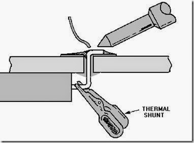
Before heat is applied to solder the joint, a thermal shunt is attached to sensitive component leads (diodes, transistors, and ICs). A thermal shunt is used to conduct heat away from the component. Because of its large heat content and high thermal conductivity, copper is usually used to make thermal shunts. Aluminum also has good conductivity but a smaller heat content; it is also used to conduct heat, especially if damage from the physical weight of the clamp is possible. Many types, shapes, and sizes of thermal shunts are available. The most commonly used is the clamp design; this is a spring clip (similar to an alligator clip) that easily fastens onto the part lead, as shown in figure 3-16.
Figure 3-16.—Thermal shunt.
APPLICATION OF SOLDER AND SOLDERING IRON TIP.—Before solder is applied to the joint, the surface temperature of the parts being soldered is increased above the solder melting point. In general, the soldering iron is applied to the point of greatest mass at the connection. This increases the heat in the parts to be soldered. Solder is then applied to a clean, fluxed, and properly heated surface. When properly applied, the solder melts and flows without direct contact with the heat source and provides a smooth, even surface that feathers to a thin edge.
Molten solder forms between the tip and the joint, creating a heat bridge or thermal linkage. This heat bridge causes the tip to become part of the joint and allows rapid heat transfer. A solder (heat) bridge is formed by melting a small amount of solder at the junction of the tip and the mass being soldered as the iron is applied. After the tip makes contact with the lead and the pad and after the heat bridge is established, the solder is applied with a wiping motion to form the solder bond. The completed solder joint should be bright and shiny in appearance. It should have no cracks or pits, and the solder should cover the pad. Examples of preferred solder joints are shown in figure 3-17. They are referred to as full fillet joints.
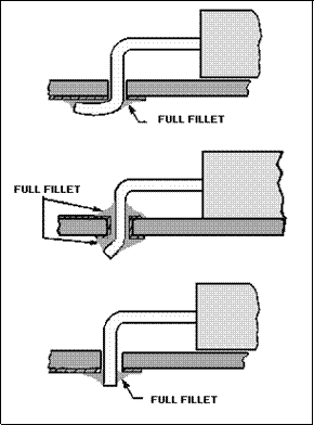 Figure 3-17.—Preferred solder joint.
When a solder joint is completed, solvent must be used to remove all flux residue. The two most highly recommended solvents, in the order of their effectiveness, are 99.5 percent pure ethyl alcohol and 99.5 percent pure isopropyl alcohol.
Q19. What is solderability?
Q20. What is the most common source of heat in electronic soldering? Q21. What determines the shape and size of a soldering iron tip?
Q22. What term describes a device used to conduct heat away from a component? Q23. What is the appearance of a properly soldered joint?
REMOVAL AND REPLACEMENT OF DIPS
In topic 1 you learned the advantages of DIPs. They are easily inserted by hand or machine and require no special spreaders, spacers, insulators, or lead-forming tools. Standard hand tools and soldering equipment can be used to remove and replace DIPS.
DIPs may be mounted on a board in two ways: (1) They may be mounted by plugging them into DIP mounting sockets that are soldered to the printed circuit boards or (2) they are soldered in place and may or may not be conformally coated. Although plug-ins are very easy to service, they lack the reliability of soldered-in units, do not meet MILSPECS, and are seldom used in military designed equipment. They are susceptible to loosening because of vibration and to poor electrical contact because of dust and dirt and corrosion.
Removal of Plug-In DIPs
To remove plug in DIPs, use an approved DIP puller, such as the one shown in figure 3-18. The puller shown is a plastic device that slips over the ends of the DIP and lifts the DIP evenly out of the socket. Before the DIP is removed, the board is marked or a sketch is made of the DIP reference mark location; then the reference mark for the replacement part will be in the proper position. The DIP is grasped with the puller and gently lifted straight out of the socket. Lifting one side or one end first results in bent leads. If the removed DIP is to be placed back in the circuit, particular care is taken in straightening bent leads to prevent breaking. To straighten bent leads, the technician grasps the wide portion of the lead with one pair of smooth-jaw needle nose pliers; with another pair, the technician then bends the lead into alignment with the other leads. Tools used for lead straightening should be cleaned with solvent to remove contaminants.
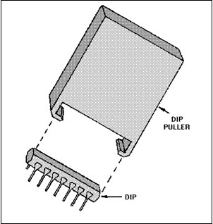 Figure 3-18.—Typical DIP puller.
To replace a plug-in DIP, the technician should clean the leads with solvent and then check the proper positioning of the reference mark. To do this, the technician holds the DIP body between the thumb and forefinger and places the part on the socket to check pin alignment. The pins are not touched. If all pins are properly aligned, the technician presses the part gently into the socket until the part is firmly seated. As pressure is applied, each pin is checked to ensure that all pins are going into the socket. If pins tend to bend, the part is removed and the pins are straightened. The socket is then inspected to make sure the holes are not obstructed. Then the process is repeated. After a thorough visual inspection, the card should be ready for testing.
Removal and Replacement of Soldered-In DIPs
The removal of soldered-in DIPs without conformal coatings is essentially the same as the removal of discrete components, except that a skipping pattern is always used. A skipping pattern is one that skips from pad to pad, never heating two pads next to each other. This reduces heat accumulation and reduces the chance of damage to the board. Of course, many more leads should be desoldered before the part can be removed. Special care must be exercised to make sure all leads are completely free before an attempt is made to lift the part off the board. If the part is known to be faulty, or if normal removal may damage the board, then the leads should be clipped. Once this has been done, desoldering can be done from both sides of the board. After the clipped leads have been desoldered, they can be removed with tweezers or pliers.
The removal of DIPs from boards with conformal coatings should be completed in the same manner as for other components. The coating should be removed using the preferred method of removal for that particular type of material. The coating should be removed from both sides of the board after masking off the work area. Particular care should be taken when removing the material from around the delicate leads. If the part is to be reused, as much of the coating should be removed from the leads as possible. As with DIPs without conformal coatings, if the part is known to be bad or if the possibility of board damage exists, the leads are clipped; the part and leads are then removed as described earlier in this section. Once the part has been removed, the work area should be completely cleaned to remove any remaining coating or solder.
The steps for replacing a soldered-in DIP are similar to those for replacing a plug-in DIP. Once the part is in position, it is soldered using the same standard used by the manufacturer, or as close to that standard as is possible with the available equipment. The joints should be soldered as quickly as possible using only as much heat as is necessary using a skipping pattern. The repaired card should then be visually inspected for defects in workmanship, and testing of the card should take place. Once the successful repair has been accomplished, a conformal coating should be applied to the work area.
REMOVAL AND REPLACEMENT OF TO PACKAGES
You should recall from chapter 1 of this module, that TO packages are mounted in two ways— plugged-in or embedded. The term plug-in, when referring to TOs, should not be confused with DIP plug-ins. TOs are normally soldered in place. You will come across sockets for TOs, but not as frequently as for DIPs. Figure 3-19 shows the methods of mounting TOs. Notice that plug-ins may either be mounted flush with the board surface or above the surface with or without a spacer. The air gap or spacer may be used by the manufacturer for a particular purpose. This type of mounting could be used for heat dissipation, short circuit protection, or to limit parasitic interaction between components. The spacer also provides additional physical support for the TO. The technician is responsible for using the same procedure as the manufacturer to replace TOs or any other components.
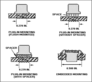 Figure 3-19.—TO mounting techniques.
The procedure for removal of plug-in TOs (with or without conformal coatings) is the same as that used for a similarly mounted DIP or discrete component. The conformal coating is removed if required. Leads are desoldered and gently lifted out of the board. Then board terminals and component leads are cleaned.
In some plug-ins, the leads must be formed before they are placed in a circuit. Care should be taken to ensure that seal damage does not occur and that formed leads do not touch the TO case. This would result in a short-circuit.
When the new part or the one that was removed is installed, the leads are slipped through the spacer if required, and the part is properly positioned (reference tab in the proper location). The leads are aligned with the terminal holes and gently pressed into position. The part is soldered into place and visually inspected. Then the card is tested and the conformal coating is replaced if required.
The removal of an imbedded TO package varies only slightly from the removal of other types of mountings. First, the work area is masked and the conformal coating is removed if required. Then the desoldering handpiece is used to remove the solder from each lead. When all leads are free, the TO is pushed out of the board. If all the leads are free, the TO should slip out of the board easily. The package should not be forced out of the board. Excessive pressure may cause additional damage. If the leads are not completely free, the leads must be clipped and removed after the package is out of the board. This process is shown in figure 3-20.
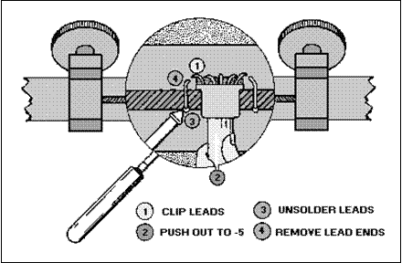 Figure 3-20.—Imbedded TO removal.
The most critical part of replacing an imbedded TO is the lead formation. The leads are formed to match the original part as closely as possible. Once the body and leads are seated, the leads can be soldered and the board inspected.
REMOVAL AND REPLACEMENT OF FLAT PACKS
Up to this point, all of the components discussed have had through-the-board leads. In addition, the removal and replacement of discrete components, DIPs, and TOs have been similar.
PLANAR-MOUNTED COMPONENTS (FLAT-PACKS)
Different techniques are used in the removal and replacement of flat packs and devices with on-the- board terminations. Lap-flow solder joints require that the technician pay particular attention to workmanship. Some of the standards of workmanship will be discussed later in this section.
Flat-Pack Removal
Prior to the removal of a flat pack, as with other ICs, a sketch should be prepared to identify the proper positioning of the part. The conformal coating should be removed as required.
To remove the flat pack, the 2M technician carefully heats the leads and lifts them free with tweezers. If the part is to be reused, special care is taken not to damage or bend the leads. The work area around the component should then be thoroughly cleaned and prepared for the new part.
Flat-Pack Replacement
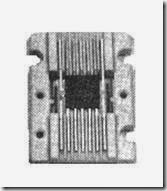
Flat packs attached to boards normally have formed and trimmed leads. Manufacturers form and trim the leads in one operation with a combination die. However, most replacement flat packs are received in a protective holder (figure 3-21) and the leads must be formed and trimmed by hand. Cost prevents equipping the repair station with the variety of tools and dies to form leads because of the variety of component configurations.
Figure 3-21.—Flat pack in protective holder.
LEAD-BENDING TECHNIQUES.—The 2M technician learns several methods of lead forming that will provide proper contact for soldering and circuit operations. The techniques used to bend leads include the use of specialized tools and such common items as flat toothpicks, bobby pins, and excess component leads. Care is taken not to stress the seal of the component during any step of the lead forming. Figure 3-22 illustrates two views, view (A) and view (B), of properly formed flat-pack leads.
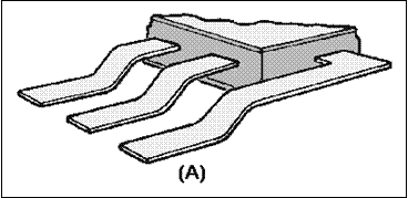 Figure 3-22A.—Properly formed flat pack leads.
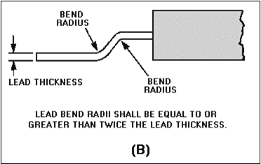 Figure 3-22B.—Properly formed flat pack leads.
Because most replacement flat packs come with leads that are longer than required, they must be trimmed before they are soldered. The removed part is used as a guide in determining lead length. Surgical scissors or scalpels are recommended for use in cutting flat-pack leads. Surgical scissors permit all leads to be cut to the required lead length in a smooth operation with no physical shock transmitted to the IC.
LAP-SOLDERING CONNECTIONS.—Before a connection is lap-soldered, the solder pads are cleaned and pretinned and the component leads are tinned. This is particularly important if they are gold plated. The IC is properly positioned on the pad areas, and the soldering process is a matter of "sweating" the two conductors together. When multilead components, such as ICs, are soldered, a skipping pattern is used to prevent excessive heat buildup in a single area of the board or component. When soldering is completed, all solder connections are thoroughly cleaned. All joints should be inspected and tested. The standards of workmanship are more specific for flat-pack installation.
Q24. When removing the component, under what circumstances may component leads be clipped? Q25. How are imbedded TOs removed once the leads are free?
Q26. How is a flat pack removed from a pcb?
Q27. How do you prevent excessive heat buildup on an area of a board when soldering multilead components?
Q28. What are the two final steps of any repair?

