PACKAGING TECHNIQUES
Once the IC has been produced, it requires a housing that will protect it from damage. This damage could result from moisture, dirt, heat, radiation, or other sources. The housing protects the device and aids in its handling and connection into the system in which the IC is used. The three most common types of packages are the modified TRANSISTOR-OUTLINE (TO) PACKAGE, the FLAT PACK, and the DUAL INLINE PACKAGE (DIP).
Transitor-Outline Package
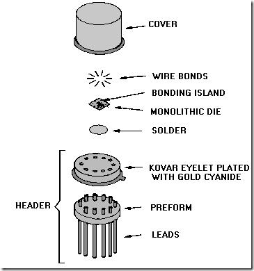
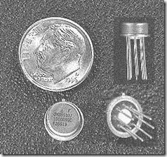
Transistor-Outline Package. The transistor-outline (TO) package was developed from early experience with transistors. It was a reliable package that only required increasing the number of leads to make it useful for ICs. Leads normally number between 2 and 12, with 10 being the most common for IC applications. Figure 1-19 is an exploded view of a TO-5 package. Once the IC has been attached to the header, bonding wires are used to attach the IC to the leads. The cover provides the necessary protection for the device. Figure 1-20 is an enlarged photo of an actual TO-5 with the cover removed. You can easily see that the handling of an IC without packaging would be difficult for a technician.
Figure 1-19.—Exploded TO-5.
Figure 1-20.—TO-5 package.
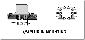
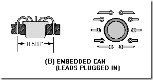
The modified TO-5 package (figure 1-21) can be either plugged into [view (A)] or embedded in [view (B)] a board. The embedding method is preferred. Whether the package is plugged in or embedded, the interconnection area of the package leads must have sufficient clearance on both sides of the board. The plug-in method does not provide sufficient clearance between pads to route additional circuitry. When the packages are embedded, sufficient space exists between the pads [because of the increased diameter of the interconnection pattern, shown at the right in view (B)] for additional conductors.
Figure 1-21A.—TO-5 mounting PLUG-IN MOUNTING
Figure 1-21B.—TO-5 mounting EMBEDDED CAN(LEADS PLUGGED IN)
Flat Pack
Many types of IC flat packs are being produced in various sizes and materials. These packages are available in square, rectangular, oval, and circular configurations with 10 to 60 external leads. They may be
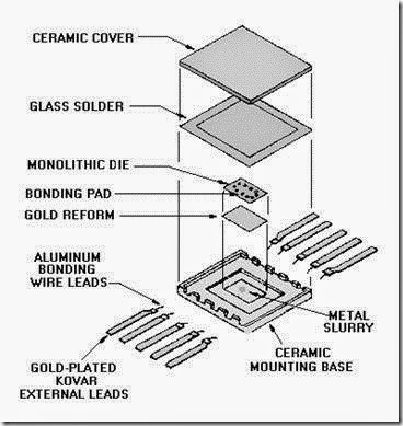
made of metal, ceramic, epoxy, glass, or combinations of those materials. Only the ceramic flat pack will be discussed here. It is representative of all flat packs with respect to general package requirements (see figure 1-22).
Figure 1-22.—Enlarged flat pack exploded view.
After the external leads are sealed to the mounting base, the rectangular area on the inside bottom of the base is treated with metal slurry to provide a surface suitable for bonding the monolithic die to the base. The lead and the metalized area in the bottom of the package are plated with gold. The die is then attached by gold-silicon bonding.
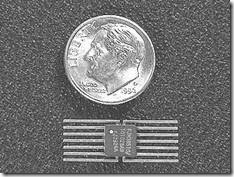
The die-bonding step is followed by bonding gold or aluminum wires between the bonding islands on the IC die and on the inner portions of the package leads. Next, a glass-soldered preformed frame is placed on top of the mounting base. One surface of the ceramic cover is coated with Pyroceram glass, and the cover is placed on top of the mounting base. The entire assembly is placed in an oven at 450 degrees Celsius. This causes the glass solder and Pyroceram to fuse and seal the cover to the mounting base. A ceramic flat pack is shown in figure 1-23. It has been opened so that you can see the chip and bonding wires.
Figure 1-23.—Typical flat pack.
Dual Inline Package
The dual inline package (DIP) was designed primarily to overcome the difficulties associated with handling and inserting packages into mounting boards. DIPs are easily inserted by hand or machine and require no spreaders, spacers, insulators, or lead-forming tools. Standard hand tools and soldering irons can be used to field-service the devices. Plastic DIPs are finding wide use in commercial applications, and a number of military systems are incorporating ceramic DIPS.
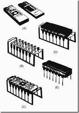
The progressive stages in the assembly of a ceramic DIP are illustrated in figure 1-24, views (A) through (E). The integrated-circuit die is sandwiched between the two ceramic elements, as shown in view (A). The element on the left of view (A) is the bottom half of the sandwich and will hold the integrated-circuit die. The ceramic section on the right is the top of the sandwich. The large well in view
(B) protects the IC die from mechanical stress during sealing operations. Each of the ceramic elements is coated with glass which has a low melting temperature for subsequent joining and sealing. View (B) shows the Kovar lead frame stamped and bent into its final shape. The excess material is intended to preserve pin alignment. The holes at each end are for the keying jig used in the final sealing operation. The lower half of the ceramic package is inserted into the lead frame shown in view (C). The die is mounted in the well and leads are attached. The top ceramic elements are bonded to the bottom element shown in view (D) and the excess material is removed from the package. View (E) is the final product.
Figure 1-24.—DIP packaging steps.
Ceramic DIPs are processed individually while plastic DIPs are processed in quantities of two or more (in chain fashion). After processing, the packages are sawed apart. The plastic package also uses a Kovar lead frame, but the leads are not bent until the package is completed. Because molded plastic is used to encapsulate the IC die, no void will exist between the cover and die, as is the case with ceramic packaging.
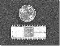
At present, ceramic DIPs are the most common of the two package types to be found in Navy microelectronic systems. Figure 1-25 shows a DIP which has been opened.
Figure 1-25.—Dual inline package (DIP).
RECENT DEVELOPMENTS IN PACKAGING
Considerable effort has been devoted to eliminating the fine wires used to connect ICs to Kovar leads. The omission of these wires reduces the cost of integrated circuits by eliminating the costs associated with the bonding process. Further, omission of the wires improves reliability by eliminating a common cause of circuit failure.
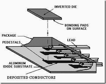
A promising packaging technique is the face-down (FLIP-CHIP) mounting method by which conductive patterns are evaporated inside the package before the die is attached. These patterns connect the external leads to bonding pads on the inside surface of the die. The pads are then bonded to appropriate pedestals on the package that correspond to those of the bonding pads on the die (figure 1-26).
Figure 1-26.—Flip-chip package.
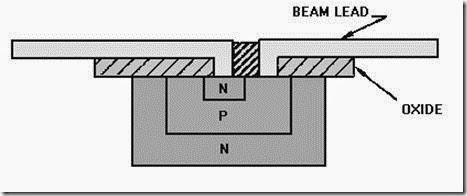
The BEAM-LEAD technique is a process developed to batch-fabricate (fabricate many at once) semiconductor circuit elements and integrated circuits with electrodes extended beyond the edges of the
wafer, as shown in figure 1-27. This type of structure imposes no electrical difficulty, and parasitic capacitance (under 0.05 picofarad per lead) is equivalent to that of a wire-bonded and brazed-chip assembly. In addition, the electrodes may be tapered to allow for lower inductance, impedance matching, and better heat conductance. The beam-lead technique is easily accomplished and does not have the disadvantages of chip brazing and wire bonding. The feasibility of this technique has been demonstrated in a variety of digital, linear, and thin-film circuits.
Figure 1-27.—Beam-lead technique.
Another advance in packaging is that of increasing the size of DIPs. General purpose DIPs have from 4 to 16 pins. Because of lsi and vlsi, manufacturers are producing DIPs with up to 64 pins. Although size is increased considerably, all the advantages of the DIP are retained. DIPs are normally designed to a particular specification set by the user.
Q29. What is the purpose of the IC package?
Q30. What are the three most common types of packages?
Q31. What two methods of manufacture are being used to eliminate bonding wires?

