INTERCONNECTIONS IN PRINTED CIRCUIT BOARDS
As electronic systems become more complex, interconnections between components also becomes more complex. As more components are added to a given space, the requirements for interconnections become extremely complicated. The selection of conductor materials, insulator materials, and component physical size can greatly affect the performance of the circuit. Poor choices of these materials can contribute to poor signals, circuit noise, and unwanted electrical interaction between components. The three most common methods of interconnection are the conventional pcb, the multilayer pcb, and the modular assembly. Each of these will be discussed in the following sections.
Conventional Printed Circuit Board
Printed circuit boards were discussed earlier in topic 1. You should recall that a conventional pcb consists of glass-epoxy insulating base on which the interconnecting pattern has been etched. The board may be single- or double-sided, depending on the number of components mounted on it. Figures 1-37 and 1-38 are examples of conventional printed circuit boards.
Multilayer Printed Circuit Board.
The multilayer printed circuit board is emerging as the solution is interconnection problems associated with high-density packaging. Multilayer boards are used to:
-
· reduce weight
-
· conserve space in interconnecting circuit modules
-
· eliminate costly and complicated wiring harnesses
-
· provide shielding for a large number of conductors
-
· provide uniformity in conductor impedance for high-speed switching systems
-
· allow greater wiring density on boards
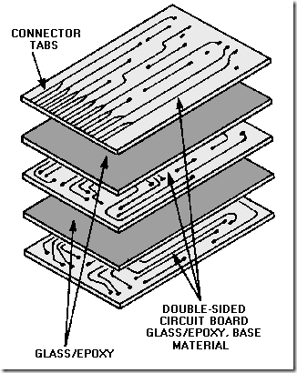
Figure 1-39 illustrates how individual boards are mated to form the multilayer unit. Although all multilayer boards are similarly constructed, various methods can be used to interconnect the circuitry from layer to layer. Three proven processes are the clearance-hole, plated-through hole, and layer build- up methods.
Figure 1-39.—Multilayer pcb.
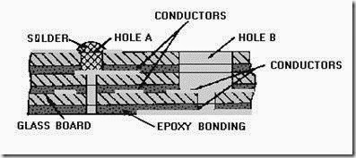
CLEARANCE-HOLE METHOD.—In the CLEARANCE-HOLE method, a hole is drilled in the copper island (terminating end) of the appropriate conductor on the top layer. This provides access to a conductor on the second layer as shown by hole A in figure 1-40. The clearance hole is filled with solder to complete the connection. Usually, the hole is drilled through the entire assembly at the connection site. This small hole is necessary for the SOLDER-FLOW PROCESS used with this interconnection method.
Figure 1-40.—Clearance-hole interconnection.
Conductors located several layers below the top are connected by using a STEPPED-DOWN HOLE PROCESS. Before assembly of a three-level board, a clearance hole is drilled down to the first layer to be interconnected. The first layer to be interconnected is predrilled with a hole smaller than those drilled in layers 1 and 2; succeeding layers to be connected have progressively smaller clearance holes. After assembly, the exposed portion of the conductors are interconnected by filling the stepped-down holes with solder, as shown by hole B in figure 1-40. The larger the number of interconnections required at one point, the larger must be the diameter of the clearance holes on the top layer. Large clearance holes on the top layer allow less space for components and reduce packaging density.
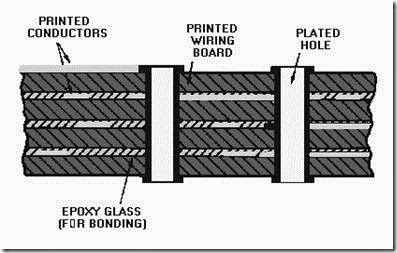
PLATED-THROUGH-HOLE METHOD.—The PLATED-THROUGH-HOLE method of
interconnecting conductors is illustrated in figure 1-41. The first step is to temporarily assemble all the layers into their final form. Holes corresponding to required connections are drilled through the entire
assembly and then the unit is disassembled. The internal walls of those holes to be interconnected are plated with metal which is 0.001 inch thick. This, in effect, connects the conductor on the board surface
through the hole itself. This process is identical to that used for standard printed circuit boards. The boards are then reassembled and permanently bonded together with heat and pressure. All the holes are plated through with metal.
Figure 1-41.—Plated through-hole interconnection.
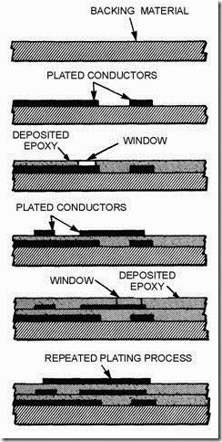
LAYER BUILD-UP METHOD.—With the LAYER BUILD-UP method, conductors and insulation layers are alternately deposited on a backing material, as shown in figure 1-42. This method produces copper interconnections between layers and minimizes the thermal expansion effects of dissimilar materials. However, reworking the internal connections in built-up layers is usually difficult, if not impossible.
Figure 1-42.—Layer build-up technique.
Advantages and Disadvantages of Printed Circuit Boards
Some of the advantages and disadvantages of printed circuit boards were discussed earlier in this topic. They are strong, lightweight, and eliminate point-to-point wiring. Multilayer printed circuit boards allow more components per card. Entire circuits or even subsystems may be placed on the same card. However, these cards do have some drawbacks. For example, all components are wired into place, repair of cards requires special training and/or special equipment, and some cards cannot be economically repaired because of their complexity (these are referred to as THROWAWAYS).
MODULAR ASSEMBLIES
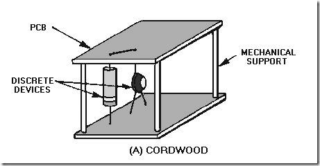
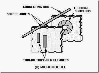
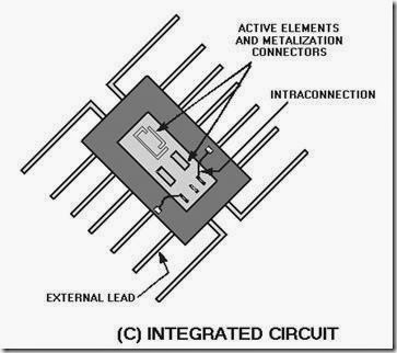
The MODULAR-ASSEMBLY (nonrepairable item) approach was devised to achieve ultra-high density packaging. The evolution of this concept, from discrete components to microelectronics, has progressed through various stages. These stages began with cordwood assemblies and functional blocks and led to complete subsystems in a single package. Examples of these configurations are shown in figure 1-43, view (A), view (B), and view (C).
Figure 1-43A.—Evolution of modular assemblies. CORDWOOD.
Figure 1-43B.—Evolution of modular assemblies. MICROMODULE.
Figure 1-43C.—Evolution of modular assemblies. INTEGRATED-CIRCUIT.
Cordwood Modules.
The cordwood assembly, shown in view (A) of figure 1-43, was designed and fabricated in various forms and sizes, depending on user requirements. This design was used to reduce the physical size and increase the component density and complexity of circuits through the use of discrete devices. However, the use of the technique was somewhat limited by the size of available discrete components used.
Micromodules
The next generation assembly was the micromodule. Designers tried to achieve maximum density in this design by using discrete components, thick- and thin-film technologies, and the insulator substrate principle. The method used in this construction technique allowed for the efficient use of space and also provided the mechanical strength necessary to withstand shock and vibration.
Semiconductor technology was then improved further with the introduction of the integrated circuit. The flat-pack IC form, shown in view (C), emphasizes the density and complexity that exists with this technique. This technology provides the means of reducing the size of circuits. It also allows the reduction of the size of systems through the advent of the lsi circuits that are now available and vlsi circuits that are being developed by various IC manufacturers.
Continuation of this trend toward microminiaturization will result in system forms that will require maintenance personnel to be specially trained in maintenance techniques to perform testing, fault isolation, and repair of systems containing complex miniature and microminiature circuits.
Q43. What are the three most common methods of interconnections?
Q44. Name the three methods of interconnecting components in multilayer printed circuit boards. Q45. What is one of the major disadvantages of multilayer printed circuit boards?
Q46. What was the earliest form of micromodule?
ENVIRONMENTAL CONSIDERATIONS
The environmental requirements of each system design are defined in the PROCUREMENT SPECIFICATION. Typical environmental requirements for an IC, for example, are shown in table 1-1. After these system requirements have been established, components, applications, and packaging forms are considered. This then leads to the most effective system form.
In the example in table 1-1, the environmental requirements are set forth as MILITARY STANDARDS for performance. The actual standard for a particular factor is in parentheses. To meet each of these standards, the equipment or component must perform adequately within the test guidelines. For example, to pass the shock test, the component must withstand a shock of 250 to 600 Gs (force of gravity). During vibration testing, the component must withstand vibrations of 5 to 15 cycles per second for 0.06 day, or about 1 1/2 hours; 16 to 25 cycles for 1 hour; and 26 to 33 cycles for 1/2 hour. Rf interference between 30 hertz and 40 gigahertz must not affect the performance of the component. Temperature and humidity factors are self-explanatory.
When selecting the most useful packaging technique, the system designer must consider not only the environmental and electrical performance requirements of the system, but the maintainability aspects as well. The system design will, therefore, reflect performance requirements of maintenance and repair personnel.
ELECTRICAL CONSIDERATIONS
The electrical characteristics of a component can sometimes be adversely affected when it is placed in a given system. This effect can show up as signal distortion, an improper timing sequence, a frequency shift, or numerous other types of unwanted interactions. Techniques designed to minimize the effects of system packaging on component performance are incorporated into system design by planners. These techniques should not be altered during your maintenance. Several of the techniques used by planners are discussed in the following sections.
Ground Planes and Shielding.
At packaging levels I and II, COPPER PLANES with voids, where feed-through is required, can be placed anywhere within the multilayer board. These planes tend to minimize interference between circuits and from external sources.
At other system levels, CROSS TALK (one signal interfering with another), rf generation within the system, and external interference are suppressed through the use of various techniques. These techniques
are shown in figure 1-44. As shown in the figure, rf shielding is used on the mating surfaces of the package, cabling is shielded, and heat sinks are provided.
Figure 1-44.—Ground planes and shielding.
Interconnection and Intraconnections
To meet the high-frequency characteristics and propagation timing required by present and future systems, the device package must not have excessive distributed capacitance and/or inductance. This type of packaging is accomplished in the design of systems using ICs and other microelectronic devices by using shorter leads internal to the package and by careful spacing of complex circuits on printed circuit boards. To take advantage of the inherent speed of the integrated circuit, you must keep the signal propagation time between circuits to a minimum. The signal is delayed approximately 1 nanosecond per foot, so reducing the distance between circuits as much as possible is necessary. This requires the use of structures, such as high-density digital systems with an emphasis on large-scale integration, for systems in the future. Also, maintenance personnel should be especially concerned with the spacing of circuits, lead dress, and surface cleanliness. These factors affect the performance of high-speed digital and analog circuits.
Q47. In what publication are environmental requirements for equipment defined?
Q48. In what publication would you find guidelines for performance of military electronic parts? Q49. Who is responsible for meeting environmental and electrical requirements of a system? Q50. What methods are used to prevent unwanted component interaction?

