SUMMARY
This topic has presented information on the development and manufacture of microelectronic devices. The information that follows summarizes the important points of this topic.
VACUUM-TUBE CIRCUITS in most modern military equipment are unacceptable because of size, weight, and power use.
Discovery of the transistor in 1948 marked the beginning of MICROELECTRONICS.
The PRINTED CIRCUIT BOARD (pcb) reduces weight and eliminates point-to-point wiring.
The INTEGRATED CIRCUITS (IC) consist of elements inseparably associated and formed on or within a single SUBSTRATE.
ICs are classified as three types: MONOLITHIC, FILM, and HYBRID.
The MONOLITHIC IC, called a chip or die, contains both active and passive elements.
FILM COMPONENTS are passive elements, either resistors or capacitors.
HYBRID ICs are combinations of monolithic and film or of film and discrete components, or any combination thereof. They allow flexibility in circuits.
Rapid development has resulted in increased reliability and availability, reduced cost, and higher element density.
LARGE-SCALE (lsi) and VERY LARGE-SCALE INTEGRATION (vlsi) allow thousands of elements in a single chip.
MONOLITHIC ICs are produced by the diffusion or epitaxial methods.
DIFFUSED elements penetrate the substrate, EPITAXIAL do not.
ISOLATION is a production method to prevent unwanted interaction between elements within a chip.
THIN-FILM ELEMENTS are produced through EVAPORATION or CATHODE SPUTTERING techniques.
THICK-FILM ELEMENTS are screened onto the substrate.
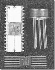
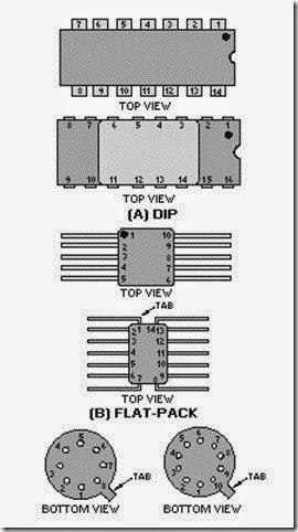
The most common types of packages for ICs are TO, FLAT PACK, and DUAL INLINE.
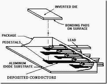
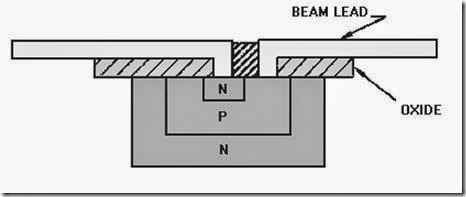
FLIP CHIPS and BEAM-LEAD CHIPS are techniques being developed to eliminate bonding wires and to improve packaging.
Large DIPs are being used to package lsi and vlsi. They can be produced with up to 64 pins and are designed to fulfill a specific need.
Viewed from the tops, DIPS and FLAT-PACK LEADS are numbered counterclockwise from the reference mark.
Viewed from the bottom, TO-5 LEADS are numbered clockwise from the tab.
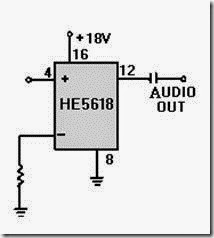
Numbers and letters on schematics and ICs identify the TYPE OF IC.
Knowledge of TERMINOLOGY used in microelectronics and of packaging concepts will aid you in becoming an effective technician.
STANDARD TERMINOLOGY has been adopted by the Navy to ease communication.
MICROELECTRONICS is that area of technology associated with electronic systems designed with extremely small parts or elements.
A MICROCIRCUIT is a small circuit which is considered as a single part composed of elements on or within a single substrate.
A MICROCIRCUIT MODULE is an assembly of microcircuits or a combination of microcircuits and discrete components packaged as a replaceable unit.
MINIATURE ELECTRONICS are card assemblies and modules composed exclusively of discrete electronic components.
SYSTEM PACKAGING refers to the design of a system, taking into account environmental and electronic characteristics, access, and maintainability.
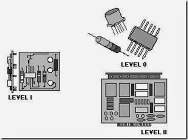
PACKAGING LEVELS 0 to IV are used to identify assemblies within a system. Packaging levels are as follows:
LEVEL 0-Nonrepairable parts (resistors, diodes, and so forth.)
LEVEL I -Submodules attached to circuit cards.
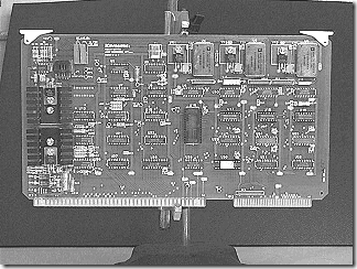
LEVEL II -Circuit cards and MOTHER BOARDS.
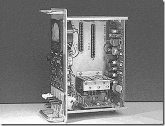
LEVEL III – Drawers.
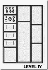
LEVEL IV – Cabinets.
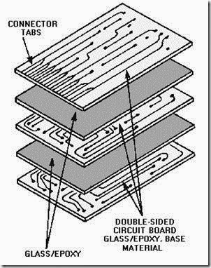
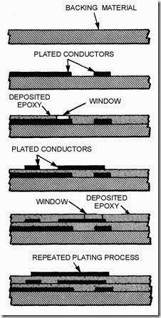
The most common METHODS OF INTERCONNECTION are the conventional pcb, the multilayer pcb, and modular assemblies.
Three methods of interconnecting circuitry in multilayer printed circuit boards are the
CLEARANCE-HOLE, the PLATED-THROUGH-HOLE, and LAYER BUILD-UP.
MODULAR ASSEMBLIES were devised to achieve high circuit density. Modular assemblies have progressed from CORDWOOD MODULES through
MICROMODULES. Micromodules consist of film components and discrete components to integrated and hybrid circuitry.
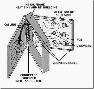
ENVIRONMENTAL FACTORS to be considered are temperature, humidity, shock, vibration, and rf interference.
ELECTRICAL FACTORS are overcome by using shielding and ground planes and by careful placement of components.
ANSWERS TO QUESTIONS Q1. THROUGH Q50.
A1. Size, weight, and power consumption. A2. The transistor and solid-state diode.
A3. Technology of electronic systems made of extremely small electronic parts or elements. A4. The Edison Effect.
A5. Transformers, capacitors, and resistors.
A6. "Rat’s nest" appearance and unwanted interaction, such as capacitive and inductive effects. A7. Rapid repair of systems and improved efficiency.
A8. Differences in performance of tubes of the same type. A9. Eliminate heavy chassis and point-to-point wiring. A10. Components soldered in place.
A11. Cordwood module.
A12. Elements inseparably associated and formed in or on a single substrate. A13. Monolithic, film, and hybrid.
A14. Monolithic ICs contain active and passive elements. Film ICs contain only passive elements.
A15. Combination of monolithic ICs and film components. A16. 1,000 to 2,000.
A17. Circuit design, component placement, suitable substrate, and depositing proper materials on substrate.
A18. Complex.
A19. Control patterns of materials on substrates. A20. Glass or ceramic.
A21. Crystal is sliced into wafers. Then ground and polished to remove any surface defect. A22. Diffusion; epitaxial growth.
A23. Diffusion penetrates substrate; epitaxial does not. A24. Electrical separation of elements.
A25. Evaporation and cathode sputtering. A26. Screening.
A27. Combination of monolithic and film elements. A28. Circuit flexibility.
A29. Protect the IC from damage; make handling easier. A30. TO, flat pack, DIP.
A31. Flip-chip, beam lead. A32. Left.
A33. Counterclockwise. A34. Reference mark. A35. Clockwise.
A36. Identify the type of IC. A37. Communication. A38. Integrated circuits. A39. Miniature.
A40. Level 0. A41. Level I. A42. Level II.
A43. Conventional printed circuit boards, multilayer printed circuit boards and modular assemblies. A44. Clearance hole, plated-through hole, and layer build-up.
A45. Difficulty of repair of internal connections. A46. Cordwood modules.
A47. Procurement specifications. A48. Military Standards.
A49. Equipment designers (planners).
A50. Ground planes, shielding, component placement.

