WAVEFORMS AND WAVE GENERATORS
LEARNING OBJECTIVES
Upon completion of this chapter you will be able to:
1. Explain the operation of a stable, monostable, and bistable multivibrators.
2. Explain the operation of a blocking oscillator.
3. Explain the operation of a sawtooth generator.
4. Explain the operation of a trapezoidal wave generator.
5. Explain how the jump voltage is produced in a trapezoidal wave generator.
WAVEFORMS
This chapter will present methods of generating waveforms. Before you begin to study how waveforms are generated, you need to know the basic characteristics of waveforms. This section will discuss basic periodic waveforms.
PERIODIC WAVEFORMS
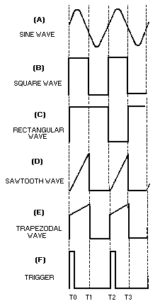
A waveform which undergoes a pattern of changes, returns to its original pattern, and repeats the same pattern of changes is called a PERIODIC waveform. Periodic waveforms are nonsinusoidal except for the sine wave. Periodic waveforms which will be discussed are the sine wave, square wave, rectangular wave, sawtooth wave, trapezoidal wave, and trigger pulses.
Sine Wave
Each completed pattern of a periodic waveform is called a CYCLE, as shown by the SINE WAVE in figure 3-1, view (A). Sine waves were presented in NEETS, Module 2, Alternating Current and Transformers, Chapter 1.
Figure 3-1.—Periodic waveforms.
Square Wave
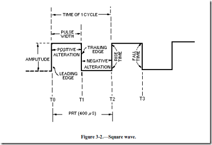
A SQUARE WAVE is shown in figure 3-1, view (B). As shown, it has two alternations of equal duration and a square presentation for each complete cycle. Figure 3-2 shows a breakdown of the square wave and is the figure you should view throughout the square wave discussion. The amplitude is measured vertically. The time for a complete cycle is measured between corresponding points on the wave (T0 to T2, or T1 to T3).
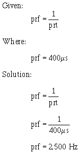
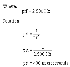
One alternation is called a PULSE. The time for one complete cycle is called the PULSE- REPETITION TIME (prt). The number of times in 1 second that the cycle repeats itself is called the PULSE-REPETITION FREQUENCY (prf) or PULSE-REPETITION RATE (prr). If each alternation in figure 3-2 is 200 microseconds (µs), the prt will be 400 microseconds, and the prf will be 2,500 hertz. The following examples are provided to illustrate the mathematical relationship between prf and prt:
You should readily see that prt is just the inverse of prf. Therefore: Given:
The length of the pulse measured in time (T0 to T1) is referred to as the PULSE WIDTH (pw). The left side of the pulse is called the LEADING EDGE and the right side is called the TRAILING EDGE.
Time is required for a voltage or current to change in amplitude. The interval of time needed for the voltage to go from 0 to 100 percent (or from 100 to 0 percent) of its maximum value is called the TRANSIENT INTERVAL. The two types of transient intervals are RISE TIME and FALL TIME. Rise time is more accurately defined as the time required for the voltage to build up from 10 percent to 90 percent of the maximum amplitude point. Fall time is the time required for the voltage to drop from 90 percent to 10 percent of the maximum amplitude point.
In this text you will be presented with information in which waveforms appear to have instantaneous rise and fall times. This is done to simplify the presentation of the material. In reality these waveforms do have rise and fall times (transient intervals).
Rectangular Wave
A rectangular wave is similar to the square wave. The difference is that in the rectangular waveform, the two alternations of the waveform are of unequal time duration. Figure 3-1, view (C), shows that the negative alternation (pulse) is shorter (in time) than the positive alternation. The negative alternation could be represented as the longer of the two alternations. Either way, the appearance is that of a rectangle.
Sawtooth Wave
The SAWTOOTH waveform is shown in figure 3-1, view (D). A sawtooth wave resembles the teeth of a saw blade. There is a rapid vertical rise of voltage from T0 to T1, which is linear (straight). At T1 this voltage abruptly falls (essentially no time used) to its previous static value. The voltage remains at this value until T2 when it again has a linear rise. You can see this action in an oscilloscope where there are two voltage input locations, vertical and horizontal. If you apply a linear voltage to the vertical input, the electron beam will be forced to move in a vertical direction on the crt. A linear voltage applied to the horizontal input will cause the electron beam to move horizontally across the crt. The application of two linear voltages, one to the vertical input and one to the horizontal input at the same time, will cause the
beam to move in both a vertical and horizontal (diagonal) direction at the same time. This then is how a sawtooth wave is made to appear on an oscilloscope. You should refer to NEETS, Module 6, Electronic Emission, Tubes, and Power Supplies, Chapter 2, for a review of oscilloscopes.
Trapezoidal Wave
A TRAPEZOIDAL wave looks like a sawtooth wave on top of a square or rectangular wave, as shown in figure 3-1, view (E). The leading edge of a trapezoidal wave is called the JUMP voltage. The next portion of the wave is the linear rise or SLOPE. The trailing edge is called the FALL or DECAY. A trapezoidal wave is used to furnish deflection current in the electromagnetic cathode ray tube and is found in television and radar display systems. Electromagnetic cathode ray tubes use coils for the deflection system, and a linear rise in current is required for an accurate horizontal display. The square or rectangular wave portion provides the jump voltage for a linear rise in current through the resistance of the coil. This will be explained further in a discussion of the trapezoidal sweep generator.
Triggers
A trigger is a very narrow pulse, as shown in figure 3-1, view (F). Trigger pulses are normally used to turn other circuits on or off.
WAVEFORM GENERATOR
Nonsinusoidal oscillators generate complex waveforms such as those just discussed. Because the outputs of these oscillators are generally characterized by a sudden change, or relaxation, these oscillators are often called RELAXATION OSCILLATORS. The pulse repetition rate of these oscillators is usually governed by the charge and discharge timing of a capacitor in series with a resistor. However, some oscillators contain inductors that, along with circuit resistance, affect the output frequency. These RC and LC networks within oscillator circuits are used for frequency determination. Within this category of relaxation oscillators are MULTIVIBRATORS, BLOCKING OSCILLATORS, and SAWTOOTH- and TRAPEZOIDAL-WAVE GENERATORS.
Many electronic circuits are not in an "on" condition all of the time. In computers, for example, waveforms must be turned on and off for specific lengths of time. The time intervals vary from tenths of microseconds to several thousand microseconds. Square and rectangular waveforms are normally used to turn such circuits on and off because the sharp leading and trailing edges make them ideal for timing purposes.
MULTIVIBRATORS
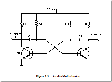
The type of circuit most often used to generate square or rectangular waves is the multivibrator. A multivibrator, as shown in figure 3-3, is basically two amplifier circuits arranged with regenerative feedback. One of the amplifiers is conducting while the other is cut off.
 When an input signal to one amplifier is large enough, the transistor can be driven into cutoff, and its collector voltage will be almost V CC. However, when the transistor is driven into saturation, its collector voltage will be about 0 volts. A circuit that is designed to go quickly from cutoff to saturation will produce a square or rectangular wave at its output. This principle is used in multivibrators.
Multivibrators are classified according to the number of steady (stable) states of the circuit. A steady state exists when circuit operation is essentially constant; that is, one transistor remains in conduction and the other remains cut off until an external signal is applied. The three types of multivibrators are the ASTABLE, MONOSTABLE, and BISTABLE.
The astable circuit has no stable state. With no external signal applied, the transistors alternately switch from cutoff to saturation at a frequency determined by the RC time constants of the coupling circuits.
The monostable circuit has one stable state; one transistor conducts while the other is cut off. A signal must be applied to change this condition. After a period of time, determined by the internal RC components, the circuit will return to its original condition where it remains until the next signal arrives.
The bistable multivibrator has two stable states. It remains in one of the stable states until a trigger is applied. It then FLIPS to the other stable condition and remains there until another trigger is applied. The multivibrator then changes back (FLOPS) to its first stable state.
Q1. What type circuit is used to produce square or rectangular waves? Q2. What type of multivibrator does not have a stable state?
Q3. What type of multvibrator has one stable state? Q4. What type of multivibrator has two stable states?
Astable Multivibrator
An astable multivibrator is also known as a FREE-RUNNING MULTIVIBRATOR. It is called free- running because it alternates between two different output voltage levels during the time it is on. The output remains at each voltage level for a definite period of time. If you looked at this output on an oscilloscope, you would see continuous square or rectangular waveforms. The astable multivibrator has two outputs, but NO inputs.
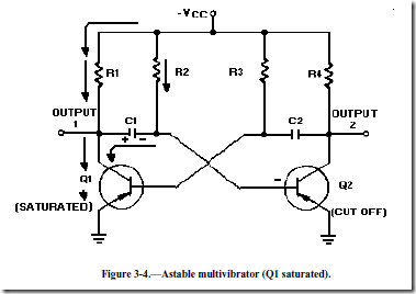
Let’s look at the multivibrator in figure 3-3 again. This is an astable multivibrator. The astable multivibrator is said to oscillate. To understand why the astable multivibrator oscillates, assume that transistor Q1 saturates and transistor Q2 cuts off when the circuit is energized. This situation is shown in figure 3-4. We assume Q1 saturates and Q2 is in cutoff because the circuit is symmetrical; that is, R1 = R4, R2 = R3, C1 = C2, and Q1 = Q2. It is impossible to tell which transistor will actually conduct when the circuit is energized. For this reason, either of the transistors may be assumed to conduct for circuit analysis purposes.
Essentially, all the current in the circuit flows through Q1; Q1 offers almost no resistance to current flow. Notice that capacitor C1 is charging. Since Q1 offers almost no resistance in its saturated state, the rate of charge of C1 depends only on the time constant of R2 and C1 (recall that TC = RC). Notice that the right-hand side of capacitor C1 is connected to the base of transistor Q2, which is now at cutoff.
Let’s analyze what is happening. The right-hand side of capacitor C1 is becoming increasingly negative. If the base of Q2 becomes sufficiently negative, Q2 will conduct. After a certain period of time, the base of Q2 will become sufficiently negative to cause Q2 to change states from cutoff to conduction. The time necessary for Q2 to become saturated is determined by the time constant R2C1.
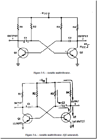
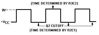
The next state is shown in figure 3-5. The negative voltage accumulated on the right side on capacitor C1 has caused Q2 to conduct. Now the following sequence of events takes place almost instantaneously. Q2 starts conducting and quickly saturates, and the voltage at output 2 changes from approximately -VCC to approximately 0 volts. This change in voltage is coupled through C2 to the base of Q1, forcing Q1 to cutoff. Now Q1 is in cutoff and Q2 is in saturation. This is the circuit situation shown in figure 3-6.
Notice that figure 3-6 is the mirror image of figure 3-4. In figure 3-6 the left side of capacitor C2 becomes more negative at a rate determined by the time constant R3C2. As the left side of C2 becomes more negative, the base of Q1 also becomes more negative. When the base of Q1 becomes negative enough to allow Q1 to conduct, Q1 will again go into saturation. The resulting change in voltage at output 1 will cause Q2 to return to the cutoff state.
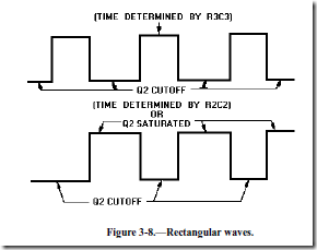
Look at the output waveform from transistor Q2, as shown in figure 3-7. The output voltage (from either output of the multivibrator) alternates from approximately 0 volts to approximately -VCC, remaining in each state for a definite period of time. The time may range from a microsecond to as much as a second or two. In some applications, the time period of higher voltage (-VCC) and the time period of lower voltage (0 volts) will be equal. Other applications require differing higher- and lower-voltage times. For example, timing and gating circuits often have different pulse widths as shown in figure 3-8.
Figure 3-7.—Square wave output from Q2.
FREQUENCY STABILITY.—Some astable multivibrators must have a high degree of frequency stability. One way to obtain a high degree of frequency stability is to apply triggers. Figure 3-9, view (A), shows the diagram of a triggered, astable multivibrator. At time T0, a negative input trigger to the base of Q1 (through C1) causes Q1 to go into saturation, which drives Q2 to cutoff. The circuit will remain in this condition as long as the base voltage of Q2 is positive. The length of time the base of Q2 will remain positive is determined by C3, R3, and R6. Observe the parallel paths for C3 to discharge.
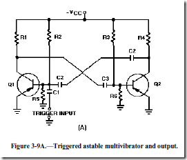 View (B) of figure 3-9 shows the waveforms associated with the circuit. At time T1, Q2 comes out of cutoff and goes into saturation. Also, Q1 is caused to come out of saturation and is cut off. The base voltage waveform of Q1 shows a positive potential that is holding Q1 at cutoff. This voltage would normally hold Q1 at cutoff until a point between T2 and T3. However, at time T2 another trigger is applied to the base of Q1, causing it to begin conducting. Q1 goes into saturation and Q2 is caused to cut off. This action repeats each time a trigger (T2, T4, T6) is applied.
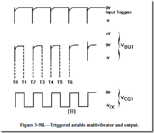 The prt of the input triggers must be shorter than the natural free-running prt of the astable multivibrator, or the trigger prf must be slightly higher than the free-running prf of the circuit. This is to make certain the triggers control the prt of the output.
Monostable Multivibrator
The monostable multivibrator (sometimes called a ONE-SHOT MULTIVIBRATOR) is a square- or rectangular-wave generator with just one stable condition. With no input signal (quiescent condition) one amplifier conducts and the other is in cutoff. The monostable multivibrator is basically used for pulse stretching. It is used in computer logic systems and communication navigation equipment.
The operation of the monostable multivibrator is relatively simple. The input is triggered with a pulse of voltage. The output changes from one voltage level to a different voltage level. The output remains at this new voltage level for a definite period of time. Then the circuit automatically reverts to its original condition and remains that way until another trigger pulse is applied to the input. The monostable multivibrator actually takes this series of input triggers and converts them to uniform square pulses, as shown in figure 3-10. All of the square output pulses are of the same amplitude and time duration.
Figure 3-10.—Monostable multivibrator block diagram.
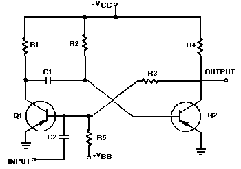
The schematic for a monostable multivibrator is shown in figure 3-11. Like the astable multivibrator, one transistor conducts and the other cuts off when the circuit is energized.
Figure 3-11.—Monostable multivibrator schematic.
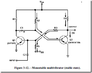
Recall that when the astable multivibrator was first energized, it was impossible to predict which transistor would initially go to cutoff because of circuit symmetry. The one-shot circuit is not symmetrical like the astable multivibrator. Positive voltage VBB is applied through R5 to the base of Q1. This positive voltage causes Q1 to cut off. Transistor Q2 saturates because of the negative voltage applied from –VCC to its base through R2. Therefore, Q1 is cut off and Q2 is saturated before a trigger pulse is applied, as shown in figure 3-12. The circuit is shown in its stable state.
Let’s take a more detailed look at the circuit conditions in this stable state (refer to figure -12). As stated above, Q1 is cut off, so no current flows through R1, and the collector of Q1 is at -VCC. Q2 is saturated and has practically no voltage drop across it, so its collector is essentially at 0 volts. R5 and R3 form a voltage divider from VBB to the ground potential at the collector of Q2. The tie point between these two resistors will be positive. Thus, the base of Q1 is held positive, ensuring that Q1 remains cutoff. Q2
will remain saturated because the base of Q2 is very slightly negative as a result of the voltage drop across R2. If the collector of Q1 is near -VCC and the base of Q2 is near ground, C1 must be charged to nearly VCC volts with the polarity shown.
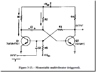
Now that all the components and voltages have been described for the stable state, let us see how the circuit operates (see figure 3-13). Assume that a negative pulse is applied at the input terminal. C2 couples this voltage change to the base of Q1 and starts Q1 conducting. Q1 quickly saturates, and its collector voltage immediately rises to ground potential. This sharp voltage increase is coupled through C1 to the base of Q2, causing Q2 to cut off; the collector voltage of Q2 immediately drops to VCC. The voltage divider formed by R5 and R3 then holds the base of Q1 negative, and Q1 is locked in saturation.
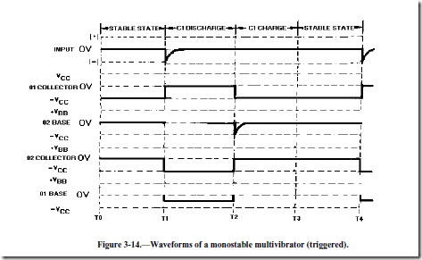
The one-shot multivibrator has now been turned on by applying a pulse at the input. It will turn itself off after a period of time. To see how it does this, look at figure 3-13 again. Q1 is held in saturation by the negative voltage applied through R3 to its base, so the circuit cannot be turned off here. Notice that the base of Q2 is connected to C1. The positive charge on C1 keeps Q2 cutoff. Remember that a positive voltage change (essentially a pulse) was coupled from the collector of Q1 when it began conducting to the base of Q2, placing Q2 in cutoff. When the collector of Q1 switches from -VCC volts to 0 volts, the charge on C1 acts like a battery with its negative terminal on the collector of Q1, and its positive terminal connected to the base of Q2. This voltage is what cuts off Q2. C1 will now begin to discharge through Q1 to ground, back through -VCC, through R2 to the other side of C1. The time required for C1 to discharge depends on the RC time constant of C1 and R2. Figure 3-14 is a timing diagram that shows the negative input pulse and the resultant waveforms that you would expect to see for this circuit description.
The only part of the operation not described so far is the short C1 charge time that occurs right after Q1 and Q2 return to their stable states. This is simply the time required for C1 to gain electrons on its left side. This charge time is determined by the R1C1 time constant.
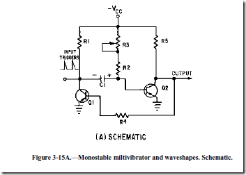
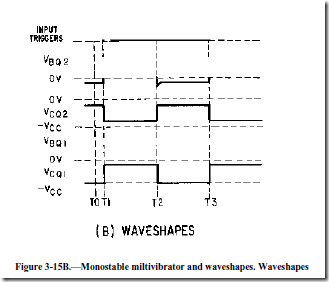
Another version of the monostable multivibrator is shown in figure 3-15. View (A) is the circuit and view (B) shows the associated waveforms. In its stable condition (T0), Q1 is cut off and Q2 is conducting. The input trigger (positive pulse at T1) is applied to the collector of Q1 and coupled by C1 to the base of Q2 causing Q2 to be cut off. The collector voltage of Q2 then goes -VCC. The more negative voltage at the collector of Q2 forward biases Q1 through R4. With the forward bias, Q1 conducts, and the collector voltage of Q1 goes to about 0 volts. C1 now discharges and keeps Q2 cut off. Q2 remains cut off until C1 discharges enough to allow Q2 to conduct again (T2). When Q2 conducts again, its collector voltage goes toward 0 volts and Q1 is cut off. The circuit returns to its quiescent state and has completed a cycle. The circuit remains in this stable state until the next trigger arrives (T3).
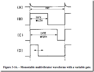
Note that R3 is variable to allow adjustment of the gate width. Increasing R3 increases the discharge time for C1 which increases the cutoff time for Q2. Increasing the value of R3 widens the gate. To decrease the gate width, decrease the value of R3. Figure 3-16 shows the relationships between the trigger and the output signal. View (A) of the figure shows the input trigger; views (B) and (C) show the different gate widths made available by R3. Although the durations of the gates are different, the duration of the complete cycle remains the same as the pulse repetition time of the triggers. View (D) of the figure illustrates that the trailing edge of the positive alternation is variable.
The reason the monostable multivibrator is also called a one-shot multivibrator can easily be seen. For every trigger pulse applied to the multivibrator, a complete cycle, or a positive and negative alternation of the output, is completed.
Q5. In an astable multivibrator, which components determine the pulse repetition frequency?
Q6. What is another name for the monostable multivibrator?
Bistable Multivibrator
As the name implies, the bistable multivibrator has two stable states. If a trigger of the correct polarity and amplitude is applied to the circuit, it will change states and remain there until triggered again. The trigger need not have a fixed prf; in fact, triggers from different sources, occurring at different times, can be used to switch this circuit.
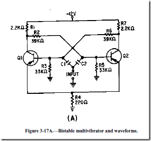
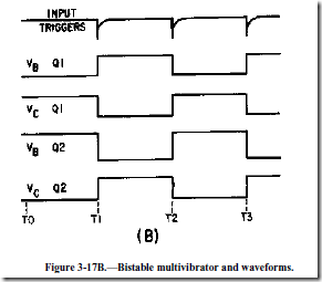
The bistable multivibrator circuit and the associated waveforms are shown in figure 3-17, views (A) and (B), respectively. In this circuit, R1 and R7 are the collector load resistors. Voltage dividers R1, R2, and R5 provide forward bias for Q2; R7, R6, and R3 provide forward bias for Q1. These resistors also couple the collector signal from one transistor to the base of the other. Observe that this is direct coupling of feedback. This type of coupling is required because the circuit depends on input triggers for operation, not on RC time constants inside the circuit. Both transistors use common emitter resistor R4 which provides emitter coupling. C1 and C2 couple the input triggers to the transistor bases.
Notice that the circuit is symmetrical; that is, each transistor amplifier has the same component values. When power is first applied, the voltage divider networks place a negative voltage at the bases of Q1 and Q2. Both transistors have forward bias and both conduct.
Due to some slight difference between the two circuits, one transistor will conduct more than the other. Assume that Q1 conducts more than Q2. The increased conduction of Q1 causes the collector voltage of Q1 to be less negative (more voltage drop across R1). This decreases the forward bias of Q2 and decreases the conduction of Q2. When Q2 conducts less, its collector voltage becomes more negative. The negative-going change at the collector of Q2 is coupled to the base of Q1 and causes Q1 to conduct even more heavily. This regenerative action continues until Q2 is cut off and Q1 is saturated. The circuit is in a stable state and will remain there until a trigger is applied to change the state.
At T1, a negative trigger is applied to both bases through C1 and C2. The trigger does not affect Q1 since it is already conducting. The trigger overcomes cutoff bias on Q2 and causes it to conduct. As Q2 goes into conduction, its collector voltage becomes positive. The positive-going change at the Q2 collector causes a reverse bias on the base of Q1. As the conduction of Q1 decreases to the cutoff point, the collector voltage becomes negative. This switching action causes a very rapid change of state with Q2 now conducting and Q1 cut off.
At T2, a negative trigger is again applied to both bases. This time, Q1 is brought into conduction and the regenerative switching action cuts off Q2. The bistable multivibrator will continue to change states as long as triggers are applied. Notice that two input triggers are required to produce one gate; one to turn it on and the other to turn it off. The input trigger frequency is twice the output frequency.
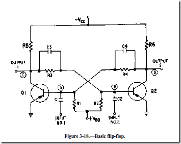
The bistable multivibrator that most technicians know is commonly known by other names: the ECCLES-JORDAN circuit and, more commonly, the FLIP-FLOP circuit (figure 3-18). The flip-flop is a bistable multivibrator, "bi" meaning two; that is, the flip-flop has two stable states. The flip-flop (f/f) can rapidly flip from one state to the other and then flop back to its original state. If a voltmeter were connected to the output of a flip-flop, it would measure either a small positive or negative voltage, or a particularly low voltage (essentially 0 volts). No matter which voltage is measured, the flip-flop would be stable. Remember, stable means that the flip-flop will remain in a particular state indefinitely. It will not change states unless the proper type of trigger pulse is applied.
Flip-flops are used in switching-circuit applications (computer logic operations) as counters, shift registers, clock pulse generators, and in memory circuits. They are also used for relay-control functions and for a variety of similar applications in radar and communications systems.
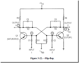
Notice that the basic flip-flop, illustrated in figure 3-18, has two inputs and two outputs. The inputs are coupled to the bases of the transistors and the outputs are coupled from the collectors of the transistors. Think of the flip-flop as two common-emitter amplifier circuits, where the output of one amplifier is connected to the input of the other amplifier, and vice-versa. Point (D) is connected through R4 to C4 to point (A). Point (A) is the input to transistor Q1. By the same token, point (C), which is the output of Q1, is connected through R3 and C3 to the input (point (B)) of transistor Q2.
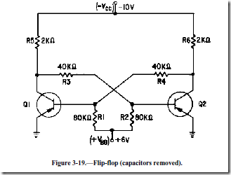
Taking a close look at the flip-flop circuit, you should be able to see how it maintains its stable condition. Typical values for the resistors and applied voltages are shown in figure 3-19. The capacitors have been removed for simplicity.
Two voltage-divider networks extend from -10 volts (V CC) to +6 volts (VBB). One voltage divider consisting of resistors R1, R4, and R6 supplies the bias voltage to the base of Q1. The other voltage divider consists of R2, R3, and R5 and supplies the bias voltage to the base of Q2.
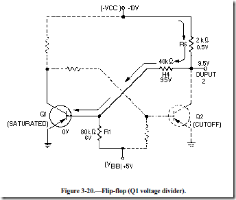
Assume that Q1 (figure 3-20) is initially saturated and Q2 is cut off. Recall that the voltage drop from the base to the emitter of a saturated transistor is essentially 0 volts. In effect, this places the base of Q1 at ground potential. The voltages developed in the voltage divider, -VCC, R6, R4, R1, and +VBB, are shown in the figure.
Since no current flows through Q2, very little voltage is dropped across R6 (approximately 0.5 volt). The voltage at output 2 would measure -9.5 volts to ground (approximately – VCC).
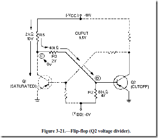
This voltage (-9.5 volts) is considered to be a HIGH output. Figure 3-21 shows the values of the other voltage-divider network.
With Q1 saturated, a large current flows through R5. The meter would measure approximately 0 volts (ground potential) at point (C). Notice that point (B) is located between point (C) (at 0 volts) and
+V BB (at +6 volts). The meter would measure a positive voltage (between 0 volts and +6 volts) at the base of Q2 (point (B)).
A positive voltage on the base of a pnp transistor will cause that transistor to cut off. If one transistor is saturated, the other must be cut off. The flip-flop is stable in this state.
The capacitors that were removed from figure 3-19 must be returned to the flip-flop as shown in figure 3-22 to change the state of the flip-flop from one condition to the other. Capacitors C3 and C4 transmit almost instantaneously any changes in voltage from the collector of one transistor to the base of the other. Capacitors C1 and C2 are input coupling capacitors.
As before, assume that transistor Q1 is saturated and transistor Q2 is cut off. Two methods are available to cause the flip-flop to change states. First, a positive-going pulse can be applied to input 1 to cause Q1 to change from saturation to cutoff. Second, the same result can be achieved by applying a negative-going pulse to input 2. Transistor Q2 would then change from Cutoff to saturation. Normally, a pulse is applied to the saturated transistor causing it to cut off. An input pulse which is of the correct polarity to change the state of the flip-flop is, as before, called a trigger pulse.
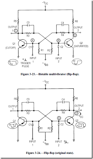
In figure 3-23 a positive-going trigger pulse has been applied to input 1. The flip-flop has now changed states; Q1 is cut off and Q2 is saturated. If a second positive-going trigger pulse is applied to input 1, it has no effect. This is because Q1 is already cut off; therefore, a positive pulse on its base has no effect. But if a positive-going trigger pulse were applied to input 2, the flip-flop would change back to its original state as shown in figure 3-24.
So far, the basic flip-flop has used only pnp transistors. It could have just as easily used npn transistors. The functional operation would not change; only the polarities required for conduction and cutoff change. As a technician, you may see either type of transistor used, npn or pnp. A symbolic block diagram is sometimes used to avoid confusion about voltage polarities.
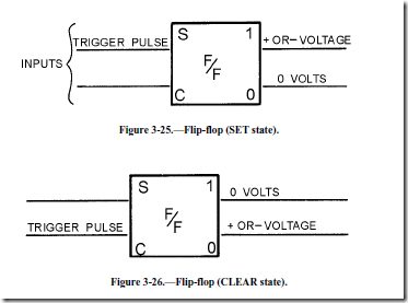
A special kind of block diagram has been adopted as a standard symbol for the flip-flop and is shown in figures 3-25 and 3-26. The two inputs are represented by the lines on the left and the outputs by the lines on the right. INPUTS to a flip-flop are S (SET) and C (CLEAR) and OUTPUTS from a flip-flop are "1" and "0." A trigger pulse applied to the SET input causes the "1" output to be a positive or negative voltage, depending on the type of transistor. At the same time, the "0" output equals 0 volts. This condition is called the SET STATE.
If a trigger pulse is applied to the CLEAR input, a positive or negative voltage is produced at the "0" output. The "1" output goes to 0 volts. This condition is called the CLEAR STATE, as shown in figure To determine what state the flip-flop is in, you can measure either the "1" or the "0" output. Measuring 0 volts at the "1" output indicates that the flip-flop is in the CLEAR state. If the "0" output is measured, a positive or negative voltage would also indicate that the flip-flop is in the CLEAR state. Either way, only one reading is necessary.
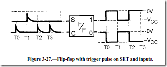
In figure 3-27, the flip-flop is in the SET state prior to T0 (negative voltage on the "1" output). Now compare the changes in output voltage at each point in time (T0, T1, T2, and T3) with the input pulse. Studying this figure should help you understand how the flip-flop works. The positive pulse at T0 on the CLEAR input shifts the f/f to the CLEAR state (negative voltage at the "0" output). At T1 a positive pulse on the SET input drives the "1" output to the SET state. At T2 a positive pulse on the CLEAR input drives the "0" output to a CLEAR state. At T3 another positive pulse is applied to the CLEAR input. This input has no effect since the f/f is already in the CLEAR state.
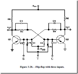
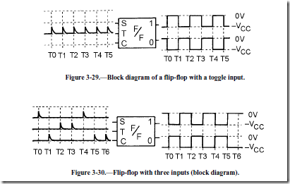
Some flip-flops use a third input lead, as shown in figure 3-28. This third input lead is called a TOGGLE (T) input. Every time a pulse is applied to the T input, the flip-flop will change states from whatever its state was previously. The two diodes (CR1, CR2) form a STEERING NETWORK. This steering network directs a positive input pulse to the saturated transistor, causing it to cut off. Negative pulses are blocked by the diodes. Note that if npn transistors were used, the diodes would have to be reversed and the TOGGLE signal would have to be negative. For example, assume that Q1 is saturated, Q2 is cut off, and a positive pulse is applied the at T input. The input pulse will be directed to both transistors. The positive pulse will not affect Q2 since it is already in cutoff. Q1 however, which is conducting, will cut off and will cause Q2 to become saturated. The transistors have reversed states. A block diagram which represents a multivibrator and its outputs with only a TOGGLE input signal is shown in figure 3-29. Studying this figure should help you understand how this flip-flop works. Each TOGGLE input causes the output to change states. Figure 3-30 shows what happens when triggers are applied to all three inputs of the flip-flop shown in figure 3-28. Assume that the flip-flop in figure 3-30 is in the CLEAR state ("1" output is 0 volts, "0" output is high) prior to T0. At T0 a trigger is applied to the set input and the flip-flop changes states. Next, the CLEAR input is triggered and the flip-flop returns to the CLEAR state at T1. A TOGGLE at T2 causes the flip-flop to change state, so it is once again SET. Another TOGGLE changes the flip-flop to the CLEAR state at T3 (notice that TOGGLE triggers flip the multivibrator regardless of its previous state). Now, a SET input trigger at T4 sets the flip-flop. The CLEAR input pulse at T5 causes the circuit to CLEAR, and the CLEAR input at T6 has no effect on the flip-flop, for it is already in the CLEAR state.
Remember, a SET input will SET the flip-flop if it is in the CLEAR state, otherwise, it will not do anything; a trigger at the CLEAR input can only CLEAR the circuit if it is SET; and a trigger applied to the TOGGLE input will cause the bistable multivibrator to change states regardless of what state it is in.
Q7. In a bistable multivibrator, how many trigger pulses are needed to produce one complete cycle in the output?
Q8. How many stable states are there for a flip-flop?
Q9. If a voltage (positive or negative) is measured on the "1" output of a flip-flop, what state is it in?

