HARTLEY OSCILLATOR
The HARTLEY OSCILLATOR is an improvement over the Armstrong oscillator. Although its frequency stability is not the best possible of all the oscillators, the Hartley oscillator can generate a wide range of frequencies and is very easy to tune. The Hartley will operate class C with self-bias for ordinary operation. It will operate class A when the output waveform must be of a constant voltage level or of a linear wave shape. The two versions of this oscillator are the series-fed and the shunt-fed. The main difference between the Armstrong and the Hartley oscillators lies in the design of the feedback (tickler) coil. A separate coil is not used. Instead, in the Hartley oscillator, the coil in the tank circuit is a split inductor. Current flow through one section induces a voltage in the other section to develop a feedback signal.
Series-Fed Hartley Oscillator
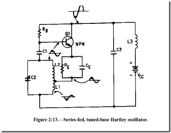
One version of a SERIES-FED HARTLEY OSCILLATOR is shown in figure 2-13. The tank circuit consists of the tapped coil (L1 and L2) and capacitor C2. The feedback circuit is from the tank circuit to the base of Q1 through the coupling capacitor C1. Coupling capacitor C1 prevents the low dc resistance of L2 from placing a short across the emitter-to-base junction and resistor RE. Capacitor C3 bypasses the sine-wave signal around the battery, and resistor RE is used for temperature stabilization to prevent thermal runaway. Degeneration is prevented by CE in parallel with RE. The amount of bias is determined by the values of RB, the emitter-to-base resistance, the small amount of dc resistance of coil L1, and the resistance of RE.
When a voltage is applied to the circuit, current from the battery flows through coil L1 and to the emitter through RE. Current then flows from the emitter to the collector and back to the battery. The surge of current through coil L1 induces a voltage in coil L2 to start oscillations within the tank circuit.
When current first starts to flow through coil L1, the bottom of L1 is negative with respect to the top of L2. The voltage induced into coil L2 makes the top of L2 positive. As the top of L2 becomes positive, the positive potential is coupled to the base of Q1 by capacitor C1. A positive potential on the base results in an increase of the forward bias of Q1 and causes collector current to increase. The increased collector current also increases the emitter current flowing through coil L1. Increased current through L1 results in more energy being supplied to the tank circuit, which, in turn, increases the positive potential at the top of the tank (L2) and increases the forward bias of Q1. This action continues until the rate of current change through coil L1 can no longer increase. The current through coil L1 and the transistor cannot continue increasing indefinitely, or the coil and transistor will burn up. The circuit must be designed, by proper selection of the transistor and associated parts, so that some point is reached when the current can no longer continue to increase. At this point C2 has charged to the potential across L1 and L2. This is shown as the heavy dot on the base waveform. As the current through L1 decreases, the voltage induced in L2 decreases. The positive potential across the tank begins to decrease and C2 starts discharging through L1 and L2. This action maintains current flow through the tapped coil and causes a decrease in the forward bias of Q1. In turn, this decrease in the forward bias of Q1 causes the collector and emitter current to decrease. At the instant the potential across the tank circuit decreases to 0, the energy of the tank circuit is contained in the magnetic field of the coil. The oscillator has completed a half cycle of operation.
Next, the magnetic field around L2 collapses as the current from C2 stops. The action of the collapsing magnetic field causes the top of L2 to become negative at this instant. The negative charge causes capacitor C2 to begin to charge in the opposite direction. This negative potential is coupled to the base of Q1, opposing its forward bias. Most transistor oscillators are operated class A; therefore, the positive and negative signals applied to the base of Q1 will not cause it to go into saturation or cutoff. When the tank circuit reaches its maximum negative value, the collector and the emitter currents will still be present but at a minimum value. The magnetic field will have collapsed and the oscillator will have completed 3/4 cycle.
At this point C2 begins to discharge, decreasing the negative potential at the top of L2 (potential will swing in the positive direction). As the negative potential applied to the base of Q1 decreases, the opposition to the forward bias also decreases. This, in effect, causes the forward bias to begin increasing, resulting in increased emitter current flowing through L1. The increase in current through L1 causes additional energy to be fed to the tank circuit to replace lost energy. If the energy lost in the tank is replaced with an equal or larger amount of energy, oscillations will be sustained. The oscillator has now completed 1 cycle and will continue to repeat it over and over again.
Shunt-Fed Hartley Oscillator
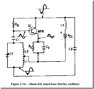
A version of a SHUNT-FED HARTLEY OSCILLATOR is shown in figure 2-14. The parts in this circuit perform the same basic functions as do their counterparts in the series-fed Hartley oscillator. The difference between the series-fed and the shunt-fed circuit is that dc does not flow through the tank circuit. The shunt-fed circuit operation is essentially the same as the series-fed Hartley oscillator. When voltage is applied to the circuit, Q1 starts conducting. As the collector current of Q1 increases, the change (increase) is coupled through capacitor C3 to the tank circuit, causing it to oscillate. C3 also acts as an isolation capacitor to prevent dc from flowing through the feedback coil. The oscillations at the collector will be coupled through C3 (feedback) to supply energy lost within the tank.
Q-12. What is the main difference between the Armstrong oscillator and the Hartley oscillator? Q-13. What is the difference between the series-fed and the shunt-fed Hartley oscillator? COLPITTS OSCILLATOR
Both the Armstrong and the Hartley oscillators have a tendency to be unstable in frequency because of junction capacitance. In comparison, the COLPITTS OSCILLATOR has fairly good frequency stability, is easy to tune, and can be used for a wide range of frequencies. The large value of split capacitance is in parallel with the junctions and minimizes the effect on frequency stability.
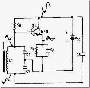
The Colpitts oscillator is very similar to the shunt-fed Hartley oscillator, except that two capacitors are used in the tank circuit instead of a tapped coil (figure 2-15). The Hartley oscillator has a tap between two coils, while the Colpitts has a tap between two capacitors. You can change the frequency of the Colpitts either by varying the inductance of the coil or by varying the capacitance of the two capacitors in the tank circuit. Notice that no coupling capacitor is used between the tank circuit and the base of Q1. Capacitors C1 and C2 of the tank circuit are in parallel with the input and the output interelement capacitance (capacitance between emitter, base, and collector) of the transistor. Thus the input and the output capacitive effect can be minimized on the tank circuit and better frequency stability can be obtained than with the Armstrong or the Hartley oscillator.
Figure 2-15.—Colpitts oscillator.
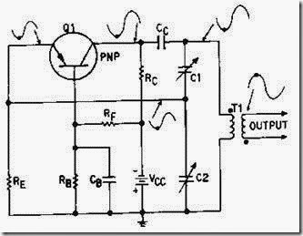
Figure 2-16 shows a common-base Colpitts oscillator using a pnp transistor as the amplifying device. Notice in this version of the Colpitts oscillator that regenerative feedback is obtained from the tank circuit and applied to the emitter. Base bias is provided by resistor RB and RF. Resistor R C is the collector load resistor. Resistor RE develops the input signal and also acts as the emitter swamping resistor. The tuned circuit consists of C1 and C2 in parallel with the primary winding of transformer T1. The voltage developed across C2 is the feedback voltage. Either or both capacitors may be adjusted to control the frequency. In the common-base configuration there is no phase difference between the signal at the collector and the emitter signal. Therefore, the phase of the feedback signal does not have to be changed. When the emitter swings negative, the collector also swings negative and C2 charges negatively at the junction of C1 and C2. This negative charge across C2 is fed back to the emitter. This increases the reverse bias on Q1. The collector of Q1 becomes more negative and C2 charges to a negative potential. This feedback effect continues until the collector of Q1 is unable to become any more negative. At that time the primary of T1 will act as a source because of normal tank circuit operation. As its field collapses, the tank potential will reverse and C1 and C2 will begin to discharge. As C2 becomes less negative, the reverse bias on Q1 decreases and its collector voltage swings in the positive direction. C1 and C2 will continue to discharge and then charge in a positive direction. This positive-going voltage across C2 will be fed back to the emitter as regenerative feedback. This will continue until the field around the primary of T1 collapses. At that time the collector of Q1 will be at a maximum positive value. C1 and C2 will begin to discharge and the potential at their junction will become less positive. This increases the reverse bias on Q1 and drives the collector negative, causing C1 and C2 to charge in a negative direction and to repeat the cycle.
Figure 2-16.—Common-base Colpitts oscillator.
Q-14. What is the identifying feature of a Colpitts oscillator?
RESISTIVE-CAPACITIVE (RC) FEEDBACK OSCILLATOR
As mentioned earlier, resistive-capacitive (RC) networks provide regenerative feedback and determine the frequency of operation in RESISTIVE-CAPACITIVE (RC) OSCILLATORS.
The oscillators presented in this chapter have used resonant tank circuits (LC). You should already know how the LC tank circuit stores energy alternately in the inductor and capacitor.
The major difference between the LC and RC oscillator is that the frequency-determining device in the RC oscillator is not a tank circuit. Remember, the LC oscillator can operate with class A or C biasing because of the oscillator action of the resonant tank. The RC oscillator, however, must use class A biasing because the RC frequency-determining device doesn’t have the oscillating ability of a tank circuit.
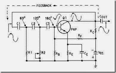
An RC FEEDBACK or PHASE-SHIFT oscillator is shown in figure 2-17. Components C1, R1, C2, R2, C3, and RB are the feedback and frequency-determining network. This RC network also provides the needed phase shift between the collector and base.
Figure 2-17.—Phase-shift oscillator.
Phase-Shift Oscillators
The PHASE-SHIFT OSCILLATOR, shown in figure 2-17, is a sine-wave generator that uses a resistive-capacitive (RC) network as its frequency-determining device.
As discussed earlier in the common-emitter amplifier configuration (figure 2-17), there is a 180-degree phase difference between the base and the collector signal. To obtain the regenerative feedback in the phase-shift oscillator, you need a phase shift of 180 degrees between the output and the input signal. An RC network consisting of three RC sections provides the proper feedback and phase inversion to provide this regenerative feedback. Each section shifts the feedback signal 60 degrees in phase.
Since the impedance of an RC network is capacitive, the current flowing through it leads the applied voltage by a specific phase angle. The phase angle is determined by the amount of resistance and capacitance of the RC section.
If the capacitance is a fixed value, a change in the resistance value will change the phase angle. If the resistance could be changed to zero, we could get a maximum phase angle of 90 degrees. But since a voltage cannot be developed across zero resistance, a 90-degree phase shift is not possible.
With a small value of resistance, however, the phase angle or phase shift is less than 90 degrees. In the phase-shift oscillator, therefore, at least three RC sections are needed to give the required 180-degree phase shift for regenerative feedback. The values of resistance and capacitance are generally chosen so that each section provides about a 60-degree phase shift.
Resistors RB, RF, and RC provide base and collector bias. Capacitor C E bypasses ac variations around the emitter resistor R E. Capacitors C1, C2, and C3 and resistors R1, R2, and R B form the feedback and phase-shifting network. Resistor R2 is variable for fine tuning to compensate for any small changes in value of the other components of the phase-shifting network.
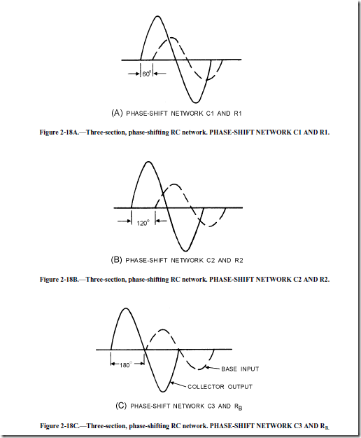
When power is applied to the circuit, oscillations are started by any random noise (random electrical variations generated internally in electronic components). A change in the flow of base current results in an amplified change in collector current which is phase-shifted the 180 degrees. When the signal is returned to the base, it has been shifted 180 degrees by the action of the RC network, making the circuit regenerative. View (A) of figure 2-18 shows the amount of phase shift produced by C1 and R1. View (B) shows the amount of phase shift produced by C2 and R2 (signal received from C1 and R1), and view (C) shows the complete phase shift as the signal leaves the RC network. With the correct amount of resistance and capacitance in the phase-shifting network, the 180-degree phase shift occurs at only one frequency. At any other than the desired frequency, the capacitive reactance increases or decreases and causes an incorrect phase relationship (the feedback becomes degenerative). Thus, the oscillator works at only one frequency. To find the resonant frequency (fr) of an RC phase shift oscillator, use the following formula:
where n is the number of RC sections.
A high-gain transistor must be used with the three-section RC network because the losses in the network are high. Using more than three RC sections actually reduces the overall signal loss within the network. This is because additional RC sections reduce the phase shift necessary for each section, and the loss for each section is lowered as the phase shift is reduced. In addition, an oscillator that uses four or more RC networks has more stability than one that uses three RC networks. In a four-part RC network, each part shifts the phase of the feedback signal by approximately 45 degrees to give the total required 180-degree phase shift.
Q-15. Which components provide the regenerative feedback signal in the phase-shift oscillator? Q-16. Why is a high-gain transistor used in the phase-shift oscillator?
Q-17. Which RC network provides better frequency stability, three-section or four-section?

