VIDEO AMPLIFIERS
As you have seen, a transistor amplifier is limited in its Frequency response. You should also remember from chapter 1 that a VIDEO AMPLIFIER should have a frequency response of 10 hertz (10 Hz) to 6 megahertz (6 MHz). The question has probably occurred to you: How is it possible to "extend" the range of Frequency response of an amplifier?
HIGH-FREQUENCY COMPENSATION FOR VIDEO AMPLIFIERS
If the frequency-response range of an audio amplifier must be extended to 6 megahertz (6 MHz) for use as a video amplifier, some means must be found to overcome the limitations of the audio amplifier. As you have seen, the capacitance of an amplifier circuit and the interelectrode capacitance of the transistor (or electronic tube) cause the higher Frequency response to be limited.
In some ways capacitance and inductance can be thought of as opposites.
As stated before, as frequency increases, capacitive reactance decreases, and inductive reactance increases. Capacitance opposes changes in voltage, and inductance opposes changes in current. Capacitance causes current to lead voltage, and inductance causes voltage to lead current.
Since frequency affects capacitive reactance and inductive reactance in opposite ways, and since it is the capacitive reactance that causes the problem with high-frequency response, inductors are added to an amplifier circuit to improve the high-frequency response. This is called HIGH-FREQUENCY COMPENSATION. Inductors (coils), when used for high-frequency compensation, are called PEAKING COILS. Peaking coils can be added to a circuit so they are in series with the output signal path or in parallel to the output signal path. Instead of only in series or parallel, a combination of peaking coils in series and parallel with the output signal path can also be used for high-frequency compensation.
As in all electronic circuits, nothing comes free. The use of peaking coils WILL increase the Frequency response of an amplifier circuit, but it will ALSO lower the gain of the amplifier.
Series Peaking
The use of a peaking coil in series with the output signal path is known as SERIES PEAKING. Figure 2-6 shows a transistor amplifier circuit with a series peaking coil. In this figure, R1 is the input-signal-developing resistor. R2 is used for bias and temperature stability of Q1. C1 is the bypass capacitor for R2. R3 is the load resistor for Q1 and develops the output signal. C2 is the coupling capacitor which couples the output signal to the next stage. "Phantom" capacitor COUT represents the output capacitance of the circuit, and "phantom" capacitor CIN represents the input capacitance of the next stage.
Figure 2-6. – Series peaking coil.
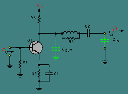
You know that the capacitive reactance of COUT and CIN will limit the high-Frequency response of the circuit. L1 is the series peaking coil. It is in series with the output-signal path and isolates COUT from CIN.
R4 is called a "swamping" resistor and is used to keep L1 from overcompensating at a narrow range of frequencies. In other words, R4 is used to keep the frequency-response curve flat. If R4 were not used with L1, there could be a "peak" in the frequency-response curve. (Remember, L1 is called a peaking coil.)
Shunt Peaking
If a coil is placed in parallel (shunt) with the output signal path, the technique is called SHUNT PEAKING. Figure 2-7 shows a circuit with a shunt peaking coil. With the exceptions of the "phantom" capacitor and the inductor, the components in this circuit are the same as those in figure 2-6. R1 is the input-signal-developing resistor. R2 is used for bias and temperature stability. C1 is the bypass capacitor for R2. R3 is the load resistor for Q1 and develops the output signal. C2 is the coupling capacitor which couples the output signal to the next stage.
Figure 2-7. – Shunt peaking coil.
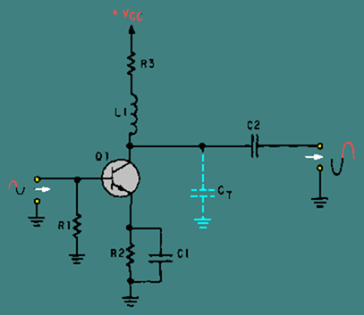
The "phantom" capacitor, CT, represents the total capacitance of the circuit. Notice that it tends to couple the output signal to ground.
L1 is the shunt peaking coil. While it is in series with the load resistor (R3), it is in parallel (shunt) with the output-signal path.
Since inductive reactance increases as frequency increases, the reactance of L1 develops more output signal as the frequency increases. At the same time, the capacitive reactance of CT is decreasing as frequency increases. This tends to couple more of the output signal to ground. The increased inductive reactance counters the effect of the decreased capacitive reactance and this increases the high-Frequency response of the amplifier.
Combination Peaking
You have seen how a series peaking coil isolates the output capacitance of an amplifier from the input capacitance of the next stage. You have also seen how a shunt peaking coil will counteract the effects of the total capacitance of an amplifier. If these two techniques are used together, the combination is more effective than the use of either one alone. The use of both series and shunt peaking coils is known as COMBINATION PEAKING. An amplifier circuit with combination peaking is shown in figure 2-8. In figure 2-8 the peaking coils are L1 and L2. L1 is a shunt peaking coil, and L2 is a series peaking coil.
Figure 2-8. – Combination peaking.
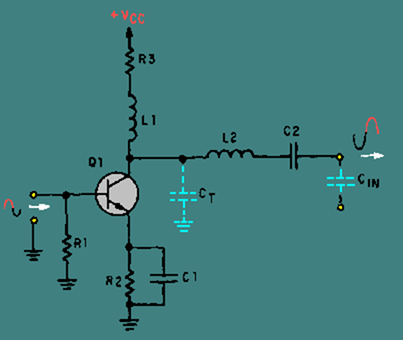
The "phantom" capacitor CT represents the total capacitance of the amplifier circuit. "Phantom" capacitor CIN represents the input capacitance of the next stage. Combination peaking will easily allow an amplifier to have a high-Frequency response of 6 megahertz (6 MHz).
Q.8 What is the major factor that limits the high-Frequency response of an amplifier circuits?
Q.9 What components can be used to increase the high-Frequency response of an amplifier?
Q.10 What determines whether these components are considered series or shunt?
Q.11 What is the arrangement of both series and shunt components called?
Back
Home
Up
Next
LOW-FREQUENCY COMPENSATION FOR VIDEO AMPLIFIERS
Now that you have seen how the high-Frequency response of an amplifier can be extended to 6 megahertz (6 MHz), you should realize that it is only necessary to extend the low-Frequency response to 10 hertz (10 Hz) in order to have a video amplifier.
Once again, the culprit in low-Frequency response is capacitance (or capacitive reactance). But this time the problem is the coupling capacitor between the stages.
At low frequencies the capacitive reactance of the coupling capacitor (C2 in figure 2-8) is high. This high reactance limits the amount of output signal that is coupled to the next stage. In addition, the RC network of the coupling capacitor and the signal-developing resistor of the next stage cause a phase shift in the output signal. (Refer to NEETS, module 2, for a discussion of phase shifts in RC networks.) Both of these problems (poor low-Frequency response and phase shift) can be solved by adding a parallel RC network in series with the load resistor. This is shown in figure 2-9.
Figure 2-9. – Low frequency compensation network.
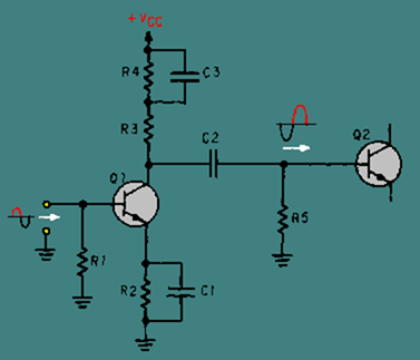
The complete circuitry for Q2 is not shown in this figure, as the main concern is the signal-developing resistor (R5) for Q2. The coupling capacitor (C2) and the resistor (R5) limit the low-Frequency response of the amplifier and cause a phase shift. The amount of the phase shift will depend upon the amount of resistance and capacitance. The RC network of R4 and C3 compensates for the effects of C2 and R5 and extends the low-frequency response of the amplifier.
At low frequencies, R4 adds to the load resistance (R3) and increases the gain of the amplifier. As frequency increases, the reactance of C3 decreases. C3 then provides a path around R4 and the gain of the transistor decreases. At the same time, the reactance of the coupling capacitor (C2) decreases and more signal is coupled to Q2.
Because the circuit shown in figure 2-9 has no high-frequency compensation, it would not be a very practical video amplifier.
TYPICAL VIDEO-AMPLIFIER CIRCUIT
There are many different ways in which video amplifiers can be built. The particular configuration of a video amplifier depends upon the equipment in which the video amplifier is used. The circuit shown in figure 2-10 is only one of many possible video-amplifier circuits. Rather than reading about what each component does in this circuit, you can see how well you have learned about video amplifiers by answering the following questions. You should have no problem identifying the purpose of the components because similar circuits have been explained to you earlier in the text.
Figure 2-10. – Video amplifier circuit.
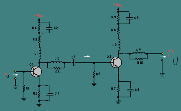
The following questions refer to figure 2-10.
Q.12 What component in an amplifier circuit tends to limit the low-Frequency response of the amplifier?
Q.13 What is the purpose of L3?
Q.14 What is the purpose of C1?
Q.15 What is the purpose of R4?
Q.16 What is the purpose of L2?
Q.17 What is the purpose of R5?
Q.18 What component(s) is/are used for high-frequency compensation for Q1?
Q.19 What component(s) is/are used for low-frequency compensation for Q2?
Back
Home
Up
Next
RADIO-FREQUENCY AMPLIFIERS
Now that you have seen the way in which a broadband, or video, amplifier can be constructed, you may be wondering about radio-frequency (rf) amplifiers. Do they use the same techniques? Are they just another type of broadband amplifier?
The answer to both questions is "no." Radio-frequency amplifiers use different techniques than video amplifiers and are very different from them.
Before you study the specific techniques used in rf amplifiers, you should review some information on the relationship between the input and output impedance of an amplifier and the gain of the amplifier stage.
AMPLIFIER INPUT/OUTPUT IMPEDANCE AND GAIN
You should remember that the gain of a stage is calculated by using the input and output signals. The formula used to calculate the gain of a stage is:

Voltage gain is calculated using input and output voltage; current gain uses input and output current; and power gain uses input and output power. For the purposes of our discussion, we will only be concerned with voltage gain.
Figure 2-11 shows a simple amplifier circuit with the input- and output-signal-developing impedances represented by variable resistors. In this circuit, C1 and C2 are the input and output coupling capacitors. R1 represents the impedance of the input circuit. R2 represents the input-signal-developing impedance, and R3 represents the output impedance.
Figure 2-11. – Variable input and output impedances.
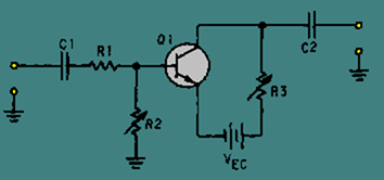
R1 and R2 form a voltage-divider network for the input signal. When R2 is increased in value, the input signal to the transistor (Q1) increases. This causes a larger output signal, and the gain of the stage increases.
Now look at the output resistor, R3. As R3 is increased in value, the output signal increases. This also increases the gain of the stage.
As you can see, increasing the input-signal-developing impedance, the output impedance, or both will increase the gain of the stage. Of course there are limits to this process. The transistor must not be overdriven with too high an input signal or distortion will result.
With this principle in mind, if you could design a circuit that had maximum impedance at a specific frequency (or band of frequencies), that circuit could be used in an rf amplifier. This FREQUENCY-DETERMINING NETWORK could be used as the input-signal-developing impedance, the output impedance, or both. The rf amplifier circuit would then be as shown in figure 2-12.
Figure 2-12. – Semiblock diagram of rf amplifier.
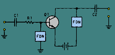
In this "semi-block" diagram, C1 and C2 are the input and output coupling capacitors. R1 represents the impedance of the input circuit. The blocks marked FDN represent the frequency-determining networks. They are used as input-signal-developing and output impedances for Q1.
FREQUENCY-DETERMINING NETWORK FOR AN RF AMPLIFIER
What kind of circuit would act as a frequency-determining network? In general, a frequency-determining network is a circuit that provides the desired response at a particular frequency. This response could be maximum impedance or minimum impedance; it all depends on how the frequency-determining network is used. You will see more about frequency-determining networks in NEETS, module 9 – Introduction to Wave-Generation and Shaping Circuits. As you have seen, the frequency-determining network needed for an rf amplifier should have maximum impedance at the desired frequency.
Before you are shown the actual components that make up the frequency-determining network for an rf amplifier, look at figure 2-13, which is a simple parallel circuit. The resistors in this circuit are variable and are connected together (ganged) in such a way that as the resistance of R1 increases, the resistance of R2 decreases, and vice versa.
Figure 2-13. – Parallel variable resistors (ganged).
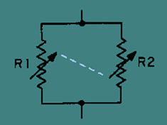
If each resistor has a range from 0 to 200 ohms, the following relationship will exist between the individual resistances and the resistance of the network (RT). (All values are in ohms, RT rounded off to two decimal places. These are selected values; there are an infinite number of possible combinations.)
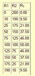
![]() As you can see, this circuit has maximum resistance (RT) when the individual resistors are of equal value. If the variable resistors represented impedances and if components could be found that varied their impedance in the same way as the ganged resistors in figure 2-13 , you would have the frequency-determining network needed for an rf amplifier.
As you can see, this circuit has maximum resistance (RT) when the individual resistors are of equal value. If the variable resistors represented impedances and if components could be found that varied their impedance in the same way as the ganged resistors in figure 2-13 , you would have the frequency-determining network needed for an rf amplifier.
There are components that will vary their impedance (reactance) like the ganged resistors. As you know, the reactance of an inductor and a capacitor vary as frequency changes. As frequency increases, inductive reactance increases, and capacitive reactance decreases.
At some frequency, inductive and capacitive reactance will be equal. That frequency will depend upon the value of the inductor and capacitor. If the inductor and capacitor are connected as a parallel LC circuit, you will have the ideal frequency-determining network for an rf amplifier.
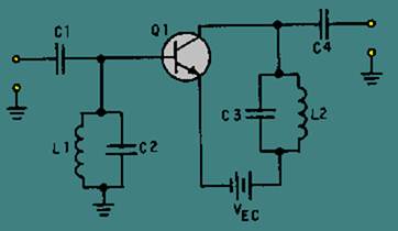
The parallel LC circuit used as a frequency-determining network is called a TUNED CIRCUIT. This circuit is "tuned" to give the proper response at the desired frequency by selecting the proper values of inductance and capacitance. A circuit using this principle is shown in figure 2-14 which shows an rf amplifier with parallel LC circuits used as frequency-determining networks. This rf amplifier will only be effective in amplifying the frequency determined by the parallel LC circuits.
Figure 2-14. – Simple rf amplifier.
In many electronic devices, such as radio or television receivers or radar systems, a particular frequency must be selected from a band of frequencies. This could be done by using a separate rf amplifier for each frequency and then turning on the appropriate rf amplifier. It would be more efficient if a single rf amplifier could be "tuned" to the particular frequency as that frequency is needed. This is what happens when you select a channel on your television set or tune to a station on your radio. To accomplish this "tuning," you need only change the value of inductance or capacitance in the parallel LC circuits (tuned circuits).
In most cases, the capacitance is changed by the use of variable capacitors. The capacitors in the input and output portions of all the rf amplifier stages are ganged together in order that they can all be changed at one time with a single device, such as the tuning dial on a radio. (This technique will be shown on a schematic a little later in this chapter.)
Q.20 If the input-signal-developing impedance of an amplifier is increased, what is the effect on the gain?
Q.21 If the output impedance of an amplifier circuit is decreased, what is the effect on the gain?
Q.22 What is the purpose of a frequency-determining network in an rf amplifier?
Q.23 Can a parallel LC circuit be used as the frequency-determining network for an rf amplifier?
Q.24 How can the frequency be changed in the frequency-determining network?
Back
Home
Up
Next
RF AMPLIFIER COUPLING
Figure 2-14 and the other circuits you have been shown use capacitors to couple the signal in to and out of the circuit (C1 and C4 in figure 2-14). As you remember from chapter 1, there are also other methods of coupling signals from one stage to another. Transformer coupling is the most common method used to couple rf amplifiers. Transformer coupling has many advantages over RC coupling for rf amplifiers; for example, transformer coupling uses fewer components than capacitive coupling. It can also provide a means of increasing the gain of the stage by using a step-up transformer for voltage gain. If a current gain is required, a step-down transformer can be used.
You should also remember that the primary and secondary windings of a transformer are inductors. With these factors in mind, an rf amplifier could be constructed like the one shown in figure 2-15.
Figure 2-15. – Transformer-coupled rf amplifier.
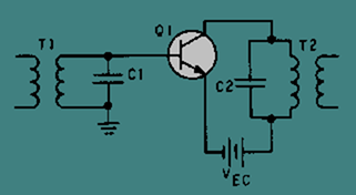
In this circuit, the secondary of T1 and capacitor C1 form a tuned circuit which is the input-signal-developing impedance. The primary of T2 and capacitor C2 are a tuned circuit which acts as the output impedance of
Q1. (Both T1 and T2 must be rf transformers in order to operate at rf frequencies.)
The input signal applied to the primary of T1 could come from the previous stage or from some input device, such as a receiving antenna. In either case, the input device would have a capacitor connected across a coil to form a tuned circuit. In the same way, the secondary of T2 represents the output of this circuit. A capacitor connected across the secondary of T2 would form a parallel LC network. This network could act as the input-
Email address: First name: Last name: Join Integrated Publishing’s Discussion GroupOrder this information on CD-RomOrder this information in Print (Hardcopy).
signal-developing impedance for the next stage, or the network could represent some type of output device, such as a transmitting antenna.
The tuned circuits formed by the transformer and capacitors may not have the bandwidth required for the amplifier. In other words, the bandwidth of the tuned circuit may be too "narrow" for the requirements of the amplifier. (For example, the rf amplifiers used in television receivers usually require a bandwidth of 6 MHz.)
One way of "broadening" the bandpass of a tuned circuit is to use a swamping resistor. This is similar to the use of the swamping resistor that was shown with the series peaking coil in a video amplifier. A swamping resistor connected in parallel with the tuned circuit will cause a much broader bandpass. (This technique and the theory behind it are discussed in more detail in NEETS, module 9.)
Another technique used to broaden the bandpass involves the amount of coupling in the transformers. For transformers, the term "coupling" refers to the amount of energy transferred from the primary to the secondary of the transformer. This depends upon the number of flux lines from the primary that intersect, or cut, the secondary. When more flux lines cut the secondary, more energy is transferred.
Coupling is mainly a function of the space between the primary and secondary windings. A transformer can be loosely coupled (having little transfer of energy), optimumly coupled (just the right amount of energy transferred), or overcoupled (to the point that the flux lines of primary and secondary windings interfere with each other).
Figure 2-16, (view A) (view B) (view C), shows the effect of coupling on frequency response when parallel LC circuits are made from the primary and secondary windings of transformers.
Figure 2-16A. – Effect of coupling on Frequency response. LOOSE COUPLING
Figure 2-16B. – Effect of coupling on Frequency response. OPTIMUM COUPLING
Figure 2-16C. – Effect of coupling on Frequency response. OVER-COUPLING

In view (A) the transformer is loosely coupled; the Frequency response curve shows a narrow bandwidth. In view (B) the transformer has optimum coupling; the bandwidth is wider and the curve is relatively flat. In view (C) the transformer is overcoupled; the Frequency response curve shows a broad bandpass, but the curve "dips" in the middle showing that these frequencies are not developed as well as others in the bandwidth.
Optimum coupling will usually provide the necessary bandpass for the frequency-determining network (and therefore the rf amplifier). For some uses, such as rf amplifiers in a television receiver, the bandpass available from optimum coupling is not wide enough. In these cases, a swamping resistor (as mentioned earlier) will be used with the optimum coupling to broaden the bandpass.
COMPENSATION OF RF AMPLIFIERS
Now you have been shown the way in which an rf amplifier is configured to amplify a band of frequencies and the way in which an rf amplifier can be "tuned" for a particular band of frequencies. You have also seen some ways in which the bandpass of an rf amplifier can be adjusted. However, the frequencies at which rf amplifiers operate are so high that certain problems exist.
One of these problems is the losses that can occur in a transformer at these high frequencies. Another problem is with interelectrode capacitance in the transistor. The process of overcoming these problems is known as COMPENSATION.
Transformers in RF Amplifiers
As you recall from NEETS, module 1, the losses in a transformer are classified as copper loss, eddy-current loss, and hysteresis loss. Copper loss is not affected by frequency, as it depends upon the resistance of the winding and the current through the winding. Similarly, eddy-current loss is mostly a function of induced voltage rather than the frequency of that voltage. Hysteresis loss, however, increases as frequency increases.
Hysteresis loss is caused by the realignment of the magnetic domains in the core of the transformer each time the polarity of the magnetic field changes. As the frequency of the a.c. increases, the number of shifts in the magnetic field also increases (two shifts for each cycle of a.c.);
therefore, the "molecular friction" increases and the hysteresis loss is greater. This increase in hysteresis loss causes the efficiency of the transformer (and therefore the amplifier) to decrease. The energy that goes into hysteresis loss is taken away from energy that could go into the signal.
RF TRANSFORMERS, specially designed for use with rf, are used to correct the problem of excessive hysteresis loss in the transformer of an rf amplifier. The windings of rf transformers are wound onto a tube of nonmagnetic material and the core is either powdered iron or air. These types of cores also reduce eddy-current loss.
Neutralization of RF Amplifiers
The problem of interelectrode capacitance in the transistor of an rf amplifier is solved by NEUTRALIZATION. Neutralization is the process of counteracting or "neutralizing" the effects of interelectrode capacitance.
Figure 2-17 shows the effect of the base-to-collector interelectrode capacitance in an rf amplifier. The "phantom" capacitor (CBC) represents the interelectrode capacitance between the base and the collector of Q1. This is the interelectrode capacitance that has the most effect in an rf amplifier. As you can see, CBC causes a degenerative (negative) feedback which decreases the gain of the amplifier. (There are some special cases in which CBC can cause regenerative (positive) feedback. In this case, the technique described below will provide negative feedback which will accomplish the neutralization of the amplifier.)
Figure 2-17. – Interelectrode capacitance in an rf amplifier.
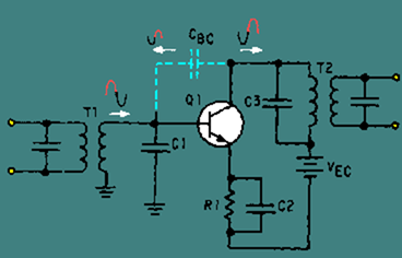
As you may recall, unwanted degenerative feedback can be counteracted (neutralized) by using positive feedback. This is exactly what is done to neutralize an rf amplifier.
Positive feedback is accomplished by the use of a feedback capacitor. This capacitor must feed back a signal that is in phase with the signal on the base of Q1. One method of doing this is shown in figure 2-18.
Figure 2-18. – Neutralized rf amplifier.
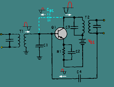
In figure 2-18, a feedback capacitor (C4) has been added to neutralize the amplifier. This solves the problem of unwanted degenerative feedback. Except for capacitor C4, this circuit is identical to the circuit shown in figure 2-17. (When CBC causes regenerative feedback, C4 will still neutralize the amplifier. This is true because C4 always provides a feedback signal which is 180 degrees out of phase with the feedback signal caused by CBC.)
Q.25 What is the most common form of coupling for an rf amplifier?
Q.26 What are two advantages of this type of coupling?
Q.27 If current gain is required from an rf amplifier, what type of component should be used as an output coupling element?
Q.28 What problem is caused in an rf amplifier by a loosely coupled transformer?
Q.29 How is this problem corrected?
Q.30 What problem is caused by overcoupling in a transformer?
Q.31 What method provides the widest bandpass?
Q.32 What two methods are used to compensate for the problems that cause low gain in an rf amplifier?
Q.33 What type of feedback is usually caused by the base-to-collector interelectrode capacitance? Q.34 How is this compensated for?
Back
Home
Up
Next
