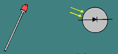
Photodiode
Figure 3-31. – Photodiode.
A second optoelectronic device that conducts current when exposed to light is the PHOTOTRANSISTOR. A phototransistor, however, is much more sensitive to light and produces more output current for a given light intensity that does a photodiode. Figure 3-32 shows one type of phototransistor, which is made by placing a photodiode in the base circuit of an NPN transistor. Light falling on the photodiode changes the base current of the transistor, causing the collector current to be amplified. Phototransistors may also be of the PNP type, with the photodiode placed in the base-collector circuit.
Figure 3-32. – Phototransistor.
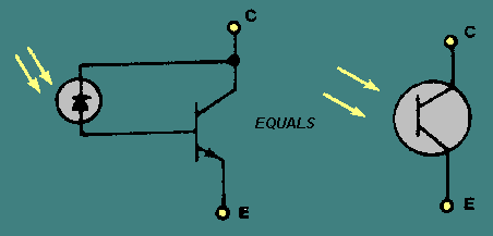
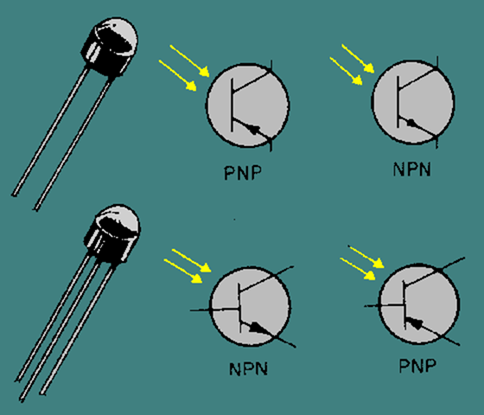
Figure 3-33 illustrates the schematic symbols for the various types of phototransistors. Phototransistors may be of the two-terminal type, in which the light intensity on the photodiode alone determines the amount of conduction. They may also be of the three-terminal type, which have an added base lead that allows an electrical bias to be applied to the base. The bias allows an optimum transistor conduction level, and thus compensates for ambient (normal room) light intensity.
Figure 3-33. – 2-terminal and 3-terminal phototransistors.
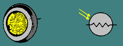
An older device that uses light in a way similar to the photodiode is the photoconductive cell, or PHOTOCELL, shown with its schematic symbol in figure 3-34. Like the photodiode, the photocell is a light-controlled variable resistor. However, a typical light-to-dark resistance ratio for a photocell is 1:1000. This means that its resistance could range from 1000 ohms in the light to 1000 kilohms in the dark, or from 2000 ohms in the light to 2000 kilohms in the dark, and so forth. Of course, other ratios are also available. Photocells are used in various types of control and timing circuits as, for example, the automatic street light controllers in most cities.
Figure 3-34. – Photocell.
The photovoltaic cell, or solar cell, is a device which converts light energy into electrical energy. An example of a solar cell and its schematic symbol are shown in figure 3-35. The symbol is similar to that of a battery. The device itself acts much like a battery when exposed to light and produces about .45 volt across its terminals, with current capacity determined by its size. As with batteries, solar cells may be connected in series or parallel to produce higher voltages and currents. The device is finding widespread application in communications satellites and solar-powered homes.
Figure 3-35. – Solar cell.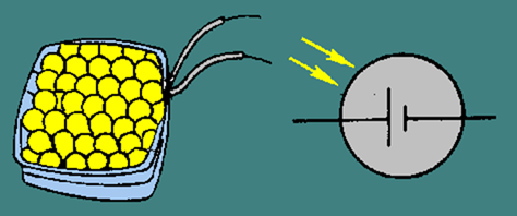
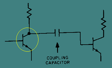
When it is necessary to block the voltage between one electronic circuit and another, and transfer the signal at the same time, an amplifier coupling capacitor is often used as shown in figure 3-36. Although this method of coupling does block dc between the circuits, voltage isolation is not complete. A newer method, making use of optoelectronic devices to achieve electrical isolation, is the optical coupler, shown in figure 3-37. The coupler is composed of an LED and a photodiode contained in a light-conducting medium. As the polarity signs in figure 3-37 show, the LED is forward biased, while the photodiode is reverse biased. When the input signal causes current through the LED to increase, the light produce by the LED increases. This increased light intensity causes current flow through the photodiode to increase. In this way, changes in input current produce proportional changes in the output, even though the two circuits are electrically isolated.
Figure 3-36. – Dc blocking with a coupling capacitor.
Figure 3-37. – Optical coupler.
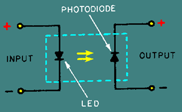
The optical coupler is suitable for frequencies in the low megahertz range. The photodiode type shown above can handle only small currents; however, other types of couplers, combining phototransistors with the SCR, can be used where more output is required. Optical couplers are replacing transformers in low-voltage and low-current applications. Sensitive digital circuits can use the coupler to control large current and voltages with low-voltage logic levels.
Q.19 What type of bias is required to cause an LED to produce light?
Q.20 When compared to incandescent lamps, what is the power requirement of an LED?
Q.21 In a common anode, seven-segment LED display, an individual LED will light if a negative voltage is applied to what element?
Q.22 What is the resistance level of a photodiode in total darkness?
Q.23 What type of bias is required for proper operation of a photodiode?
Q.24 What is a typical light-to-dark resistance ratio for a photocell?
Q.25 What semiconductor device produces electrical energy when exposed to light?
Back
Home
Up
Next
TRANSISTORS
Transistors are semiconductor devices with three or more terminals. The operation of normal transistors has already been discussed, but there are several transistors with special properties that should be explained. As with diodes, a discussion of all the developments in the transistor field would be impossible. The unijunction transistor (UJT) and the field effect transistor (FET) will be discussed because of their widespread application in Navy equipment. Many other special transistors have been developed and will be discussed in later NEETS modules.
The Unijunction Transistor (UJT)
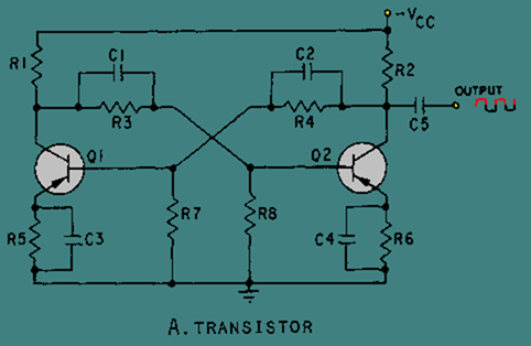
The UNIJUNCTION TRANSISTOR (UJT), originally called a double-based diode, is a three-terminal, solid-state device that has several advantages over conventional transistors. It is very stable over a wide range of temperatures and allows a reduction of components when used in place of conventional transistors. A comparison is shown in figure 3-38. View A is a circuit using conventional transistors, and view B is the same circuit using the UJT. As you can see, the UJT circuit has fewer components. Reducing the number of components reduces the cost, size, and probability of failure.
Figure 3-38A. – Comparison of conventional transistors and UJT circuits.
Figure 3-38B. – Comparison of conventional transistors and UJT circuits.

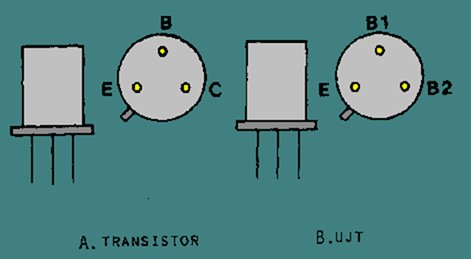
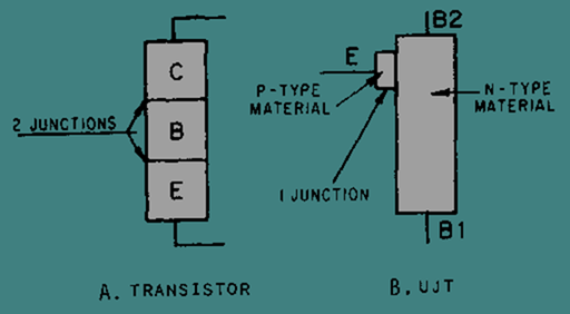
The physical appearance of the UJT is identical to that of the common transistor. As shown in figure 3-39, both have three leads and the same basic shape; the tab on the case indicates the emitter on both devices. The UJT, however, has a second base instead of a collector.
Figure 3-39. – Transistor and UJT.
As indicated in the block diagram shown in views A and B of figure 3-40, the lead differences are even more pronounced. Unlike the transistor, the UJT has only one PN junction. The area between base 1 and base 2 acts as a resistor when the UJT is properly biased. A conventional transistor needs a certain bias level between the emitter, base, and collector for proper conduction. The same principle is true for the UJT; it needs a certain bias level between the emitter and base 1 and also between base 1 and base 2 for proper conduction.
Figure 3-40. – Transistor and UJT structure.
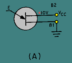
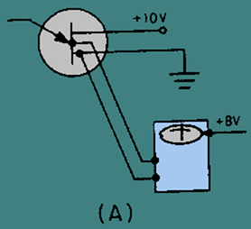
The normal bias arrangement for the UJT is illustrated in figure 3-41, view A. A positive 10 volts is placed on base 2 and a ground on base 1. The area between base 1 and base 2 acts as a resistor. If a reading were taken between base 1 and base 2, the meter would indicate the full 10 volts as shown in view B. Theoretically, if one meter lead were connected
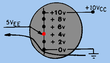
to base 1 and the other lead to some point between base 1 and base 2, the meter would read some voltage less than 10 volts. This concept is illustrated in figure 3-42, view A. View B is an illustration of the voltage levels at different points between the two bases. The sequential rise in voltage is called a voltage gradient.
Figure 3-41A. – UJT biasing.
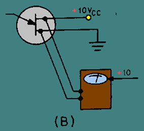
Figure 3-42A. – UJT voltage gradient.
Figure 3-42B. – UJT voltage gradient.
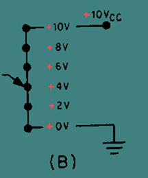
The emitter of the UJT can be viewed as the wiper arm of a variable resistor. If the voltage level on the emitter is more positive than the voltage gradient level at the emitter-base material contact point, the UJT is forward biased. The UJT will conduct heavily (almost a short circuit) from base 1 to the emitter. The emitter is fixed in position by the manufacturer. The level of the voltage gradient therefore depends upon the amount of bias voltage, as shown in figure 3-43.
Figure 3-43. – Forward bias point on UJT voltage gradient.
If the voltage level on the emitter is less positive than the voltage gradient opposite the emitter, the UJT is reverse biased. No current will flow from base 1 to the emitter. However, a small current, called reverse current, will flow from the emitter to base 2. The reverse current is caused by the impurities used in the construction of the UJT and is in the form of minority carriers.
More than 40 distinct types of UJTs are presently in use. One of the most common applications is in switching circuits. They are also used extensively in oscillators and wave-shaping circuits.
Q.26 The UJT has how many PN junctions?
Q.27 The area between base 1 and base 2 in a UJT acts as what type of common circuit component?
Q.28 The sequential rise in voltage between the two bases of the UJT is called what?
Q.29 What is the normal current path for a UJT?
Back
Home
Up
Next
Field Effect Transistors
Although it has brought about a revolution in the design of electronic equipment, the bipolar (PNP/NPN) transistor still has one very undesirable characteristic. The low input impedance associated with its base-emitter junction causes problems in matching impedances between interstage amplifiers.
For years, scientists searched for a solution that would combine the high input impedance of the vacuum tube with the many other advantages of the transistor. The result of this research is the FIELD-EFFECT TRANSISTOR (FET). In contrast to the bipolar transistor, which uses bias current between base and emitter to control conductivity, the FET uses voltage to control an electrostatic field within the transistor. Because the FET is voltage-controlled, much like a vacuum tube, it is sometimes called the "solid-state vacuum tube."
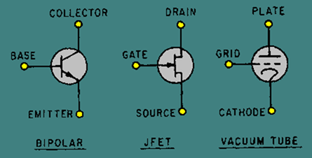
The elements of one type of FET, the junction type (JFET), are compared with the bipolar transistor and the vacuum tube in figure 3-44. As the figure shows, the JFET is a three-element device comparable to the other two. The "gate" element of the JFET corresponds very closely in operation to the base of the transistor and the grid of the vacuum tube. The "source" and "drain" elements of the JFET correspond to the emitter and collector of the transistor and to the cathode and plate of the vacuum tube.
Figure 3-44. – Comparison of JFET, transistor, and vacuum tube symbols.
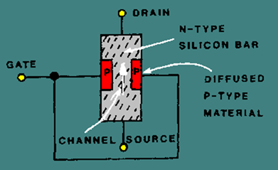
The construction of a JFET is shown in figure 3-45. A solid bar, made either of N-type or P-type material, forms the main body of the device. Diffused into each side of this bar are two deposits of material of the opposite type from the bar material, which form the "gate." The portion of the bar between the deposits of gate material is of a smaller cross section than the rest of the bar and forms a "channel" connecting the source and the drain. Figure 3-45 shows a bar of N-type material and a gate of P-type material. Because the material in the channel is N-type, the device is called an N-channel JFET.
Figure 3-45. – JFET structure.
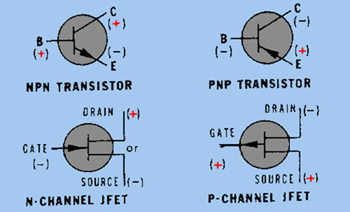
In a P-channel JFET, the channel is made of P-type material and the gate of N-type material. In figure 3-46, schematic symbols for the two types of JFET are compared with those of the NPN and PNP bipolar transistors. Like the bipolar transistor types, the two types of JFET differ only in the configuration of bias voltages required and in the direction of the arrow within the symbol. Just as it does in transistor symbols, the arrow in a JFET symbol always points towards the N-type material. Thus the symbol of the N-channel JFET shows the arrow pointing toward the drain/source channel, whereas the P-channel symbol shows the arrow pointing away from the drain/source channel toward the gate.
Figure 3-46. – Symbols and bias voltages for transistors and JFET.
The key to FET operation is the effective cross-sectional area of the channel, which can be controlled by variations in the voltage applied to the gate. This is demonstrated in the figures which follow.
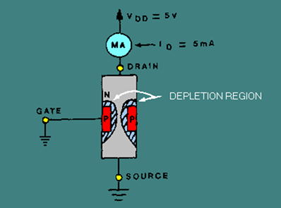
Figure 3-47 shows how the JFET operates in a zero gate bias condition. Five volts are applied across the JFET so that current flows through the bar from source to drain, as indicated by the arrow. The gate terminal is tied to ground. This is a zero gate bias condition. In this condition, a typical bar represents a resistance of about 500 ohms. A milliammeter, connected in series with the drain lead and dc power, indicates the amount of current flow. With a drain supply (VDD) of 5 volts, the milliammeter gives a drain current (ID) reading of 10 milliamperes. The voltage and current subscript letters (VDD, ID) used for an FET correspond to the elements of the FET just as they do for the elements of transistors.
Figure 3-47. – JFET operation with zero gate bias.
In figure 3-48, a small reverse-bias voltage is applied to the gate of the JFET. A gate-source voltage (VGG) of negative 1 volt applied to the P-type gate material causes the junction between the P- and N-type material to become reverse biased. Just as it did in the varactor diode, a reverse-bias condition causes a "depletion region" to form around the PN junction of the JFET. Because this region has a reduced number of current carriers, the effect of reverse biasing is to reduce the effective cross-sectional area of the "channel." This reduction in area increases the source-to-drain resistance of the device and decreases current flow.
Figure 3-48. – JFET with reverse bias.
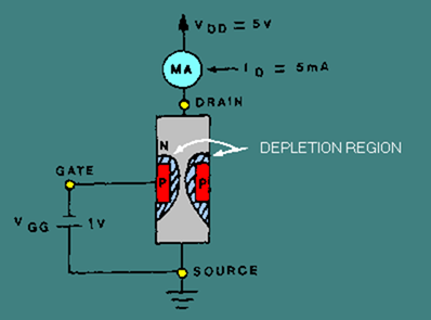
The application of a large enough negative voltage to the gate will cause the depletion region to become so large that conduction of current through the bar stops altogether. The voltage required to reduce drain current (ID) to zero is called "pinch-off" voltage and is comparable to "cut-off" voltage in a vacuum tube. In figure 3-48, the negative 1 volt applied, although not large enough to completely stop conduction, has caused the drain current to decrease markedly (from 10 milliamperes under zero gate bias conditions to 5 milliamperes). Calculation shows that the 1-volt gate bias has also increased the resistance of the JFET (from 500 ohms to 1 kilohm). In other words, a 1-volt change in gate voltage has doubled the resistance of the device and cut current flow in half.
These measurements, however, show only that a JFET operates in a manner similar to a bipolar transistor, even though the two are constructed differently. As stated before, the main advantage of an FET is that its input impedance is significantly higher than that of a bipolar transistor. The higher input impedance of the JFET under reverse gate bias conditions can be seen by connecting a microammeter in series with the gate-source voltage (VGG), as shown in figure 3-49.
Figure 3-49. – JFET input impedance.
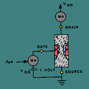
With a VGG of 1 volt, the microammeter reads .5 microamps. Applying Ohm’s law (1V ¸ .5mA) illustrates that this very small amount of current flow results in a very high input impedance (about 2 megohms). By contrast, a bipolar transistor in similar circumstances would require higher current flow (e.g., .1 to -1 mA), resulting in a much lower input impedance (about 1000 ohms or less). The higher input impedance of the JFET is possible because of the way reverse-bias gate voltage affects the cross-sectional area of the channel.
The preceding example of JFET operation uses an N-channel JFET. However, a P-channel JFET operates on identical principles. The differences between the two types are shown in figure 3-50.
Back
Home
Up
Next

