Current flow in the operational circuit
You can compute the values for view (C) and prove that point A in that circuit is also at virtual ground.
The whole point is that the inverting input to the operational amplifier shown in figure 3-13 is at virtual ground since it is at 0 volts (for all practical purposes). Because the inverting input is at 0 volts, there will be no current (for all practical purposes) flowing into the operational amplifier from the connection point of R1 and R2.
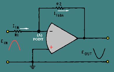
Given these conditions, the characteristics of this circuit are determined almost entirely by the values of R1 and R2. Figure 3-15 should help show how the values of R1 and R2 determine the circuit characteristics.
Figure 3-15. – Current flow in the operational circuit.
NOTE: It should be stressed at this point that for purpose of explanation the operational amplifier is a theoretically perfect amplifier. In actual practice we are dealing with less than perfect. In the practical operational amplifier there will be a slight input current with a resultant power loss. This small signal can be measured at the theoretical point of virtual ground. This does not indicate faulty operation.
The input signal causes current to flow through R1. (Only the positive half cycle of the input signal is shown and will be discussed.) Since the voltage at the inverting input of the operational amplifier is at 0 volts, the input current (Iin) is computed by: The output signal (which is opposite in phase to the input signal) causes a feedback current (Ifdbk) to flow through R2. The left-hand side of R2 is at 0 volts (point A) and the right-hand side is at Eout. Therefore, the feedback current is computed by:

(The minus sign indicates that Eout is 180 degrees out of phase with Ein and should not be confused with output polarity.)
Since no current flows into or out of the inverting input of the operational amplifier, any current reaching point A from R1 must flow out of point A through R2. Therefore, the input current (Iin) and the feedback current (Ifdbk) must be equal. Now we can develop a mathematical relationship between the input and output signals and R1 and R2.
Mathematically: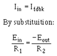
If you multiply both sides of the equation by R1:
If you divide both sides of the equation by Eout:

By inverting both sides of the equation:
You should recall that the voltage gain of a stage is defined as the output voltage divided by the input voltage:![]()
Therefore, the voltage gain of the inverting configuration of the operational amplifier is expressed by the equation:![]()
(As stated earlier, the minus sign indicates that the output signal is 180 degrees out of phase with the input signal.)
Noninverting Configuration
Figure 3-16 shows a noninverting configuration using an operational amplifier. The input signal (Ein) is applied directly to the noninverting (+) input of the operational amplifier. Feedback is provided by coupling part of the output signal (Eout) back to the inverting (-) input of the operational amplifier. R1 and R2 act as voltage divider that allows only a part of the output signal to be applied as feedback (Efdbk).
Figure 3-16. – Noninverting configuration.
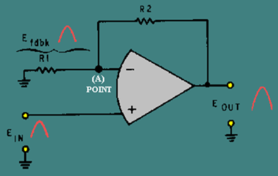
Notice that the input signal, output signal, and feedback signal are all in phase. (Only the positive alternation of the signal is shown.) It may appear as if the feedback is regenerative (positive) because the feedback and input signals are in phase. The feedback is, in reality, degenerative (negative) because the input signals is applied to the noninverting input and the feedback signal is applied to the inverting input, (Remember, that the operational amplifier will react to the difference between the two inputs.)
Just as in the inverting configuration, the feedback signal is equal to the input signal (for all practical purposes). This time, however, the feedback signal is in phase with the input signal.
Therefore:![]()
Given this condition, you can calculate the gain of the stage in terms of the resistors (R1 and R2).
The gain of the stage is defined as: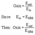
The feedback signal (Efdbk) can be shown in terms of the output signal (Eout) and the voltage divider (R1 and R2). The voltage divider has the output signal on one end and ground (0 volts) on the other end. The feedback signal is that part of the output signal developed by R1 (at point A). Another way to look at it is that the feedback signal is the amount of output signal left (at point A) after part of the output signal has been dropped by R2. In either case, the feedback signal (Efdbk) is the ratio of R1 to the entire voltage divider (R1 + R2) multiplied by the output signal (Eout).
Mathematically, the relationship of the output signal, feedback signal, and voltage divider is:
If you divide both sides of the equation by Eout:
By inverting both sides of the equation:

Separating the right-hand side:

Remember:
Therefore, by substitution:
You can now see that the gain of the noninverting configuration is determined by the resistors. The formula is different from the one used for the inverting configuration, but the gain is still determined by the values of R1 and R2.
Back
Home
Up
Next
BANDWIDTH LIMITATIONS
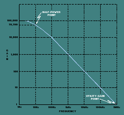
As with most amplifiers, the gain of an operational amplifier varies with frequency. The specification sheets for operational amplifiers will usually state the open-loop (no feedback) gain for d.c. (or 0 hertz). At higher frequencies, the gain is much lower. In fact, for an operational amplifier, the gain decreases quite rapidly as frequency increases.
Figure 3-17 shows the open-loop (no feedback) frequency-response curve for a typical operational amplifier. As you should remember, bandwidth is measured to the half-power points of a frequency-response curve. The frequency-response curve shows that the bandwidth is only 10 hertz with this configuration. The UNITY GAIN POINT, where the signal out will have the same amplitude as the signal in (the point at which the gain of the amplifier is 1), is 1 megahertz for the amplifier. As you can see, the Frequency response of this amplifier drops off quite rapidly.
Figure 3-17. – Open-loop frequency-response curve.
Figure 3-17 is the open-loop frequency-response curve. You have been told that most operational amplifiers are used in a closed-loop configuration. When you look at the frequency-response curve for a closed-loop configuration, one of the most interesting and important aspects of the operational amplifier becomes apparent: The use of degenerative feedback increases the bandwidth of an operational amplifier circuit.
This phenomenon is another example of the difference between the operational amplifier itself and the operational-amplifier circuit (which includes the components in addition to the operational amplifier). You should also be able to see that the external resistors not only affect the gain of the circuit, but the bandwidth as well.
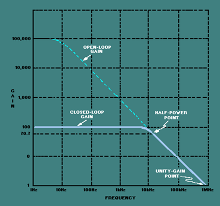
You might wonder exactly how the gain and bandwidth of a closed-loop, operational-amplifier circuit are related. Figure 3-18 should help to show you the relationship. The frequency-response curve shown in figure 3-18 is for a circuit in which degenerative feedback has been used to decrease the circuit gain to 100 (from 100,000 for the operational amplifier). Notice that the half-power point of this curve is just slightly above 10 kilohertz.
Figure 3-18. – Closed-loop frequency-response curve for gain of 100.
Now look at figure 3-19. In this case, more feedback has been used to decrease the gain of the circuit to 10. Now the bandwidth of the circuit is extended to about 100 kilohertz.
Figure 3-19. – Closed-loop frequency-response curve for gain of 10.
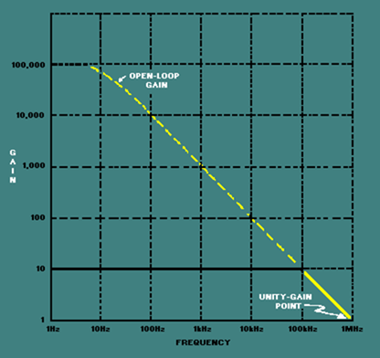
The relationship between circuit gain and bandwidth in an operational-amplifier circuit can be expressed by the GAIN-BANDWIDTH PRODUCT (GAIN X BANDWIDTH = UNITY GAIN POINT). In other words, for operational-amplifier circuits, the gain times the bandwidth for one configuration of an operational amplifier will equal the gain times the bandwidth for any other configuration of the same operational amplifier. In other words, when the gain of an operational-amplifier circuit is changed (by changing the value of feedback or input resistors), the bandwidth also changes. But the gain times the bandwidth of the first configuration will equal the gain times the bandwidth of the second configuration. The following example should help you to understand this concept.
The frequency-response curves shown in figures 3-17, 3-18, and 3-19 have a gain-bandwidth product of 1,000,000. In figure 3-17, the gain is 100,000 and the bandwidth is 10 hertz. The gain-bandwidth product is 100,000 times 10 (Hz), or 1,000,000. In figure 3-18, the gain has been reduced to 100 and the bandwidth increases to 10 kilohertz. The gain-bandwidth product is 100 times 10,000 (Hz) which is also equal to 1,000,000. In figure 3-19 the gain has been reduced to 10 and the bandwidth is 100 kilohertz. The gain-bandwidth product is 10 times 100,000 (Hz), which is 1,000,000. If the gain were reduced to 1, the bandwidth would be 1 megahertz (which is shown on the frequency-response curve as the unity-gain point) and the gain-bandwidth product would still be 1,000,000.
Q.19 What does the term "closed-loop" mean in the closed-loop configuration of an operational amplifier? In answering Q20, Q21, and Q23, select the correct response from the choices given in the parentheses.
Q.20 In a closed-loop configuration the output signal is determined by (the input signal, the feedback signal, both).
Q.21 In the inverting configuration, the input signal is applied to the (a) (inverting, noninverting) input and the feedback signal is applied to the (b) (inverting, noninverting) input.
Q.22 In the inverting configuration, what is the voltage (for all practical purposes) at the inverting input to the operational amplifier if the input signal is a 1-volt, peak-to-peak sine wave?
Q.23 In the inverting configuration when the noninverting input is grounded, the inverting input is at (signal, virtual) ground.
Q.24 In a circuit such as that shown in figure 3-15, if R1 has a value of 100 ohms and R2 has a value of 1 kilohm and the input signal is at a value of + 5 millivolts, what is the value of the output signal?
Q.25 If the unity-gain point of the operational amplifier used in question 24 is 500 kilohertz, what is the bandwidth of the circuit?
Q.26 In a circuit such as that shown in figure 3-16, if R1 has a value of 50 ohms and R2 has a value of 250 ohms and the input signal has a value of +10 millivolts, what is the value of the output signal?
Q.27 If the open-loop gain of the operational amplifier used in question 26 is 200,000 and the open-loop bandwidth is 30 hertz, what is the closed loop bandwidth of the circuit?
Back
Home
Up
Next
APPLICATIONS OF OPERATIONAL AMPLIFIERS
Operational amplifiers are used in so many different ways that it is not possible to describe all of the applications. Entire books have been written on the subject of operational amplifiers. Some books are devoted entirely to the applications of operational amplifiers and are not concerned with the theory of operation or other circuits at all. This module, as introductory material on operational amplifiers, will show you only two common applications of the operational amplifier: the summing amplifier and the difference amplifier. For ease of explanation the circuits shown for these applications will be explained with d.c. inputs and outputs, but the circuit will work as well with a.c. signals.
Summing Amplifier (Adder)
Figure 3-20 is the schematic of a two-input adder which uses an operational amplifier. The output level is determined by adding the input signals together (although the output signal will be of opposite polarity compared to the sum of the input signals).
Figure 3-20. – Two-input adder.
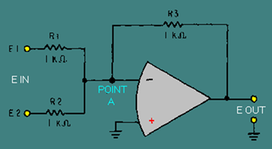
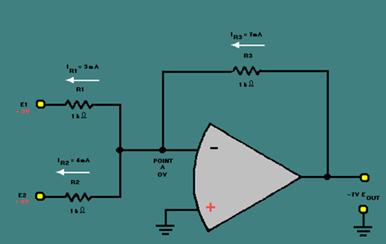
If the signal on input number one (E1) is +3 volts and the signal on input number two (E2) is +4 volts, the output signal (Eout) should be -7 volts [(+3 V) + (+4 V) = +7 V and change the polarity to get -7 V].
With +3 volts at E1 and 0 volts at point A (which is at virtual ground), the current through R1 must be 3 milliamperes.
Mathematically:
(The + sign indicates a current flow from right to left.)
By the same sort of calculation, with +4 volts at E2 and 0 volts at point A the current through R2 must be 4 milliamps.
This means that a total of 7 milliamps is flowing from point A through R1 and R2. If 7 milliamps is flowing from point A, then 7 milliamps must be flowing into point A. The 7 milliamps flowing into point A flows through R3 causing 7 volts to be developed across R3. With point A at 0 volts and 7 volts developed across R3, the voltage potential at Eout must be a -7 volts. Figure 3-21 shows these voltages and currents.
Figure 3-21. – Current and voltage in a two-input adder.
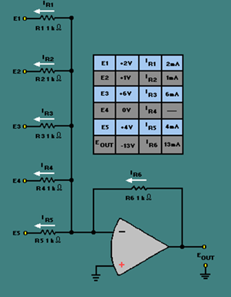
An adder circuit is not restricted to two inputs. By adding resistors in parallel to the input terminals, any number of inputs can be used. The adder circuit will always produce an output that is equal to the sum of the input signals but opposite in polarity. Figure 3-22 shows a five-input adder circuit with voltages and currents indicated.
Figure 3-22. – Five-input adder.
The previous circuits have been adders, but there are other types of summing amplifiers. A summing amplifier can be designed to amplify the results of adding the input signals. This type of circuit actually multiplies the sum of the inputs by the gain of the circuit.
Mathematically (for a three-input circuit):![]()
If the circuit gain is -10:![]()
The gain of the circuit is determined by the ratio between the feedback resistor and the input resistors. To change figure 3-20 to a summing amplifier with a gain of -10, you would replace the feedback resistor (R3)
with a 10-kilohm resistor. This new circuit is shown in figure 3-23.
Figure 3-23. – Summing amplifier.
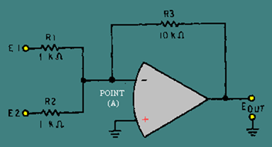
If this circuit is designed correctly and the input voltages (E1 and E2) are +2 volts and +3 volts, respectively, the output voltage (E out) should be:
To see if this output (-50 V) is what the circuit will produce with the inputs given above, start by calculating the currents through the input resistors, R1 and R2 (remember that point A is at virtual ground):
Next, calculate the current through the feedback resistor (R3):
(The minus sign indicates current flow from left to right.)
Finally, calculate the voltage dropped across R3 (which must equal the output voltage):
As you can see, this circuit performs the function of adding the inputs together and multiplying the result by the gain of the circuit.
Back
Home
Up
Next

