Introduction
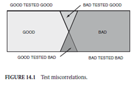
The goal of the test process for integrated circuits is to separate good devices from bad devices, and to test good devices as good. Bad devices tested as bad become yield loss, but they also represent opportunity for cost reduction as we reduce number of defects in the process. When good devices are tested as bad, overkill occurs and this directly impacts cost and profits. Finally, bad devices tested as good signal a quality problem, usually represented as defects per million (DPM) devices delivered.
Unfortunately, the test environment is not the same as the operating environment. The test process may reject good devices and may accept defective devices as good. Here lies one of the basic problems of today’s test methods, and it must be understood and addressed as we look at how to generate and test integrated circuits. Figure 14.1 shows this miscorrelation of test to use.
Bad devices are removed from good devices through a series of test techniques that enable the separation, by either voltage- or current-based testing. The match between the test process and the actual system use will not be addressed in this chapter.
Defect Types
Defects in an integrated circuit process fall into three broad categories. They are:
-
Opens or abnormally high-resistance portions of signal lines and power lines that increase the series resistance between connected points. This extra resistance slows the charging of the parasitic
 capacitance of the line, thus resulting in a time delay. These defects also degrade voltage to a transistor circuit, which reduces levels or causes delays.
-
Shorts, bridges, or resistive connections between layers of an integrated circuits, which form a resistance path in a normal insulating area. Given sufficiently low R value, the path may not be able to drive a 1 or a 0.
-
✁ Parameter variations such as threshold voltage and saturation current deviations changed by contamination, particles, implant, or process parameter changes. These usually result in speed or drive level changes.
Table 14.1 shows several types of defects and how they are introduced into an integrated circuit. It also describes electrical characteristics.
Defects, although common in integrated circuit processes, are difficult to quantify via test methods. Therefore, the industry has developed abstractions of defects called faults. Faults attempt to model the way defects manifest themselves in the test environment.
Traditional Faults and Fault Models
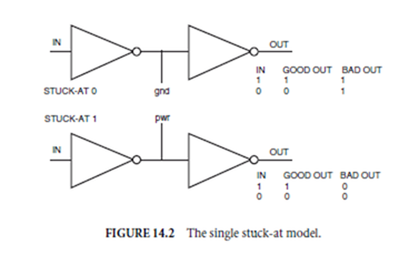
The most widely used fault model is the single stuck-at fault model. It is available in a variety of simulation environments with good support tools. The model represents a defect as a short of a signal line to a power supply line. This causes the signal to remain fixed at either a logic one or a zero. Thus, the logical result of an operation is not propagated to an output. Figure 14.2 shows the equivalent of a single stuck-at one or zero fault in a logic circuit. Although this fault model is the most common one, it was developed over 30 years ago, and does not always reflect today’s more advanced processes. Today’s very large-scale integrated (VLSI) circuits and submicron processes more commonly have failures that closely approximate bridges between signal lines. These bridges do not map well to the stuck-at fault model.
 Other proposed or available fault models include:
-
The open fault model: This model is for open circuits. Unfortunately in CMOS, missing contacts and transistors can exhibit correct behavior when switching at speed, even if some of the transistors or contacts are missing.
-
The leakage fault model: This model assumes leakage in transistors and lends itself to an IDDQ1 test technique (discussed later in this chapter).
-
Timing fault models (delay, gate and transition faults): All of these models assume a change in the AC characteristics of the circuit. Either a single gate, line, or block of circuitry is slower than needed or simulated, and this slow signal causes a problem with at-speed operation of the integrated circuit.
-
Pseudostuck-at model fault model for IDDQ: This model assumes nodes look like they are stuck at a one or zero logic level.
-
Voting fault models, and bridge models: Adjacent lines are assumed connected and the logic result is an X (unknown), or a vote with the highest drive strength circuit dominating the logic level.
-
Also for memory circuits.
-
Neighborhood pattern faults: This fault assumes operations in one memory cell will affect adjacent memory cells (usually limited to the four closest cells).
-
Coupling faults: This fault model assumes that full rows or columns couple signals into the cells or adjacent rows and columns.
-
Retention faults: These faults are similar to the open fault for logic (discussed previously). Failures to this fault model do not retain data over an extended period of time.
There are many other fault models.
It is important to realize that the stuck-at model may not necessarily catch failures and/or defects in the fabrication processes. This problem is being addressed by the computer-aided design (CAD) industry.
Today, numerous solutions are available, or on the horizon, that address the issues of fault models. Tools currently available can support delay faults. Bridging fault routines have been demonstrated in university research, and should be available from selected CAD vendors within a few years. Soon, we will not be confined to testing solely through the single stuck-at model.
Concepts of Test
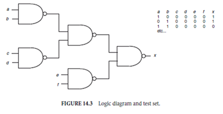
The main test method of an integrated circuit is to control and observe nodes. Doing this verifies the logical operation that ensures that the circuit is fault free. This process is usually done by generating stimulus patterns for the input and comparing the outputs to a known good state. Figure 14.3 demonstrates a classic case where a small portion of an integrated circuit is tested with a stimulus pattern set for inputs and an expected set for outputs. Note this test set is logic, not layout, dependent and checks only stuck at faults.
Types of Test
There are three basic types of test for integrated circuits. These are parametric tests, voltage tests, and current tests. Each has a place in the testing process.
Parametrics tests ensure the correct operation of the transistors (voltage and current) of the integrated circuit. Parametric tests include timing, input and output voltage, and current tests. Generally, they measure
 circuit performance. In all of these tests, numbers are associated with the measurements. Typical readings include: Tx < 334 ns, IOH < 4 mA, VOI < 0.4 V, etc.
The next major category of testing is power supply current tests. Current tests include active switching current or power test, power down test, and standby or stable quiescent current tests. This last test, often called IDDQ, will be discussed later.
The most common method of testing integrated circuits is the voltage-based test. Voltage-based test for logic operations includes functions such as placing a one on the input of an integrated circuit and ensuring that the proper one or zero appears on the output of the IC at the right time. Logical values are repeated, in most cases, at high and low operating voltage. The example in Fig. 14.3 is a voltage-based test.
Test Methods
To implement voltage based testing or any of the other types of tests, initialization of the circuit must take place, and control and observation of the internal nodes must occur. The following are four basic categories of tests:
-
External stored response testing. This is the most common form for today’s integrated circuits and it relies heavily on large IC automated test equipment (ATE).
-
Builtin-self-test (BIST). This is method of defining and building test circuity onto the integrated circuit. This technique provides stimulus patterns and observes the logical output of the integrated circuit.
-
Scan testing. Some or all of the sequential elements are converted into a shift register for control and observation purposes.
-
Parametric tests. The values of circuit parameters are directly measured. This includes the IDDQ test, which is good at detecting certain classes of defects. To implement an IDDQ test, a CMOS integrated circuit clock is stopped and the quiescent current is measured. All active circuitry must be placed in a low-current state, including all analog circuitry.
External Stored Response Testing
Figure 14.4 shows a typical integrated circuit being tested by a stored response tester. Note that the patterns for the input and output of the integrated circuit are applied by primary inputs, and the output is compared to known good response. The process of generating stored response patterns is usually done by simulation.
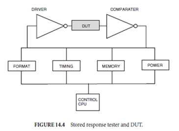 Often these patterns are trace files from the original logic simulation of the circuit. These files may be used during simulation for correct operation of the logic and later transferred to a tester for debug, circuit verification, and test. The patterns may take up considerable storage space, but the test pattern can easily detect structural and/or functional defects in an integrated circuit.
To exercise the device under test (DUT), a stored response functional tester relies on patterns saved from the logic simulation. These patterns include input and output states and must account for unknown or X states. The set of patterns for functional test can usually be captured as trace files, or change files, and then ported to the test equipment. Trace or change files capture the logic state of the DUT as its logical outputs change over time. Typically, these patterns represent the logical operation of the device under test. As such, they are good for debugging the operation and design of integrated circuits. They are not the best patterns for fault isolation or yield analysis of the device.
BIST
The most common implementation of BIST is to include a linear feedback shift register (LFSR) as an input source. An LFSR is constructed from a shift register with the least significant bit fed back to selected stages with exclusive-OR gates. This feedback mechanism creates a polynomial, which successively divides the quotient and adds back the remainder. Only certain polynomials create pseudorandom patterns. The selection of the polynomial must be carefully considered. The LFSR source, when initialized and clocked correctly, generates a pseudorandom pattern that is used for the stimulus patterns for a block of logic in an integrated circuit.
The common method of output compaction is to use a multiple input shift register (MISR). A MISR is an LFSR with the outputs of the logic block connected to the stages of the LFSR with additional exclusive- OR gates. The block of logic, if operating defect free, would give a single correct signature (see Fig. 14.5). If there is a defect in the block of logic, the resultant logic error would be captured in the output MISR. The MISR constantly divides the output with feedback to the appropriate stages such that an error will remain in the MISR until the results are read at the end of the test sequence. Because the logic states are compacted in a MISR, the results may tend to mask errors if the error repeats itself in the output, or if there are multiple errors in the block. Given a number of errors, the output could contain the correct answer even though the logic block contains errors or defects. This problem is called aliasing. For example, the output register shown in Fig. 14.5 is 20-bits long; 220 is approximately one million, which means that there is a very high chance that without an aliasing defect, the output will be the correct state of one out of a million with a fault free integrated circuit.
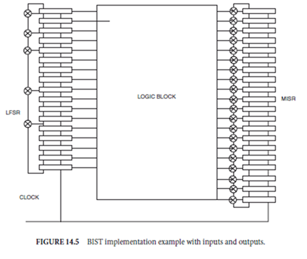 It should be noted that the example is shown for combination logic only. Sequential logic becomes more difficult as initialization, illegal states, state machines, global feedback, and many other cases must be accounted for in the generation of BIST design and patterns.
Scan
Scan is a technique where storage elements (latches and flip-flops) are changed to dual mode elements. For instance, Fig. 14.6 shows a normal flip-flop of an integrated circuit. Also shown in Fig. 14.6 is a flip-flop converted to a scan register element. During normal operation, the D input and system clock control the output of the flip-flop. During scan operation, the scan clocks are used to control shifting of data into
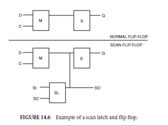 and out of the shift register. Data is shifted into and out of the master and scan latch. The slave latch can be clocked by the system clock in order to gener- D ate a signal for the required stimulation of the logic C between this scan latch and the next scan latches. Figure 14.7 shows latches and logic between latches.
This method successfully reduces the large sequential test problem to a rather simple combinatorial problem. The unfortunate problem with scan is that the area overhead is, by far, the largest of all design
for test (DFT) methods. This area increase is due to the fact that each storage element must increase in transistor count to accommodate the added function of scan.
Note that the scan latch contains extra elements for control and observation. These extra elements include the scan-clock (SC), scan-in (SI), and scan-out (SO). As shown in Fig. 14.7, the scan-clock is used to drive all scan latches. This controls the shift register function of the scan latch, and will allow a known one or zero to be set for each latch in the scan chain. For each scan clock applied, a value of one or zero is placed on the scan-in line, which is then shifted to the scan-out and the next scan-in latch. This shifting stops when the entire chain is initialized. At the end of the scan in sequence, a system clock is triggered, which launches data from the scan portion of the latch of the Q output. Then it goes through the combinational logic to the next stage D input where another system clock stores it in the latch. The next set of scan loads, and shifts out the stored value of the logic operation for comparison. If the logic operation was correct, the scan value will be correct in the shift out sequence.
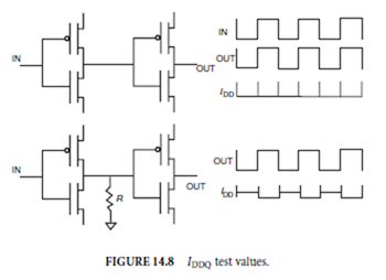
IDDQ is perhaps the simplest test concept. Figure 14.8 shows a typical dual inverter structure with a potential defect. It also shows the characteristic of IDDQ. The upper circuit is defect free, and the lower circuit has a leakage defect shown as R. IDDQ is shown for each clock cycle. Note the elevated current in the defective circuit during clock cycle A. This elevated current is called IDDQ . It is an easy way to check for most bridging and many other types of defects. The IDDQ test controls and observes approximately half of the transistors in a IC for each test. Therefore, the test is considered massively parallel and is very efficient at detecting bridge defects and partial shorts. Another consideration is the need to design for an IDDQ test. All DC paths, pullups, bus drivers, and contention paths must be designed for zero current when the clock is stopped. One single transistor remaining on, can disable the use of an IDDQ test..
Note that Vout and IDD in the defective case may be tolerable if the output voltage is sufficient to drive the next input stage. Not shown here is the timing impact of the degraded voltage. This degraded voltage will cause a time delay in the next stage.
Test Tradeoffs
To determine the best type of test, one must understand the defect types, the logical function of the integrated circuit, and test requirements. Examples of test tradeoffs are included in Table 14.2. The rows in the table correspond to the test types as listed earlier: scan, BIST, stored response, and IDDQ. The columns in the table depict certain attributes of test to be described here.
The first column is the test type. Column number two shows pattern complexity. This is the problem of generating the necessary patterns in order to fully stimulate and control the nodes of the integrated circuit. Column number three is illegal states. Often times the logic in integrated circuits, such as bidirectional bus drivers and signals, must be exclusively set one way or another. Examples include decoders, bus drivers and mutually exclusive line drivers. Tests such as scan and BIST, if not designed and implemented correctly, can damage the integrated circuit during the test process by putting the circuit into an internal contention state. Examples include two bus drivers on simultaneously when one drives high and the other drives low.
Aliasing is a common problem of BIST techniques. This is shown in column four. For example, consider a memory laid out in rows and columns and assume that one column is a complete failure. If there are multiple failures along the column, let us say 256, and if the signature length is 256, the output could possibly show a correct response even though the entire column or row of the memory is defective.
The next column shows overhead. Overhead is the amount of silicon area necessary to implement the test. Each of the areas of overhead relate to the amount of silicon area needed to implement the specific types of test methods.
The final column is the time for test generation. The unfortunate relationship here is that the techniques with the highest area overhead have the most complete control and are easiest to generate tests. Techniques with the lowest area needs have the most complex test generation problem, and take the longest time. This is a complex trade off.
Tradeoffs of Volume and Testability
It is important to forecast the volume of the integrated circuit to be manufactured prior to selecting DFT and test methods. Engineering effort is nonrecurring and can be averaged over every integrated circuit manufactured. The testing of an integrated circuit can be a simple or a complex process. The criteria used for selecting the proper test technique must include volume, expected quality, and expected cost of the integrated circuit. Time to market and/or time to shipments are key factors, as some of the test techniques for very large integrated circuits take an extremely long time.
Defining Terms
Automated test equipment (ATE): Any computer controlled equipment used to test integrated circuits.
Builtin self-test (BIST): An acronym that generally describes a design technique with input stimulus generation circuitry and output response checking circuitry.
Defect: Any error, particle, or contamination of the circuit structure. Defects may or may not result in faulty circuit operation.
Design for test (DFT): A general term which encompasses all techniques used to improve control and observation of internal nodes.
Device under test (DUT): A term used to describe the device being tested by the ATE.
Fault: The operation of a circuit in error. Usually faulty circuits are the result of defects or damage to the circuit.
Linear feedback shift register (LFSR): A method of construction of a register with feedback to generate pseudo random numbers.
Multiple input shift register (MISR): Usually an LFSR with inputs consisting of the previous stage exclusive OR’ed with input data. This method compacts the response of a circuit into a polynomial.
Scan: A design technique where sequential elements (latches, or flipflops) are chained together in a mode that allows data shifting into and out of the latches. In general, scan allows easy access to the logic between latches and greatly reduces the test generation time and effort.
References
Abramovici, M. et al. 1990. Digital Systems Testing and Testable Design. IEEE Press, New York. Needham, W.M. 1991. Designer’s Guide to Testable ASIC Devices. Van Nostrand Reinhold, New York.
van de Goor, A.J. 1991. Testing Semiconductor Memories, Theory and Practice. John Wiley & Sons, New York.
Further Information
IEEE International Test Conference (ITC). This is the largest gathering of test experts, test vendors and researchers in the world.
IEEE Design Automation Conference (DAC) held in various sites throughout the world. IEEE VLSI Test Symposium.
Test vendors of various types of equipment provide training for operation, programming, and maintenance of ATE.
CAD vendors supply a variety of simulation tools for test analysis and debugging.

