Oscillators
An oscillator is an electronic circuit designed to produce an alternating e.m.f. of known frequency and waveform. In this chapter only oscillator circuits which produce an output voltage of sinusoidal waveform will be discussed.
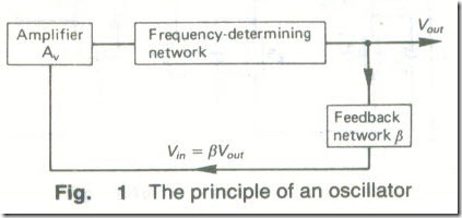
An oscillator is an amplifier that provides its own input signal, which is derived from the output signal (Fig. 1). A fraction β of the output voltage is fed back to the input. If the gain of the amplifier is Av, the output voltage is AvVin and the input voltage is Vin= βAvVin, so then
Vin (1 – βAv )= 0
The input voltage cannot be zero as an output voltage exists and therefore (1- βAv) = 0 must be zero, or
βAv = 1 (7.la)
In general, both the gain Av and the feedback ratio β are complex quantities and hence
│β │∠ Ø . │Av │ ∠θ = 1 ∠ 0° (7 .1b)
so that
│βAv │∠ Ø + θ = 1 ∠ 0° (7.lc)
This equation states the necessary requirements that must be satisfied before a circuit will oscillate: firstly, the loop gain │βAv │ must be unity, and secondly, the loop phase shift (Ø + θ) must be zero. In practice, the magnitude of the loop gain βAv . must be somewhat greater than unity or oscillations will never start.
When an oscillator is first switched on, a current surge in the frequency-determining network produces a voltage, at the required frequency of oscillation, across the network. A fraction of this voltage is fed back to the input terminals of the amplifier and is amplified to reappear across the network. A fraction of this larger voltage is then fed back to the input to be further amplified, and so on. In this way the amplitude of the signal voltage builds up until the gain of the amplifier is reduced in some way to make the loop gain unity. The bipolar transistor or FET may be biased to operate under either Class A or Class C conditions; when the former are used the loop gain is reduced either by the transistor driving into saturation or by the use of a variable feedback element. An op-amp may be used as the active element; then either saturation or a nonlinear feedback component is employed to limit the gain.
The frequency-determining section of an oscillator may consist of an LC tuned circuit, a resistance-capacitance network, or a piezoelectric crystal.
The important characteristics of an oscillator are its frequency or frequencies (if variable) of operation, its frequency stability, its amplitude stability, and the percentage distortion of its output wave form.
LC Oscillators
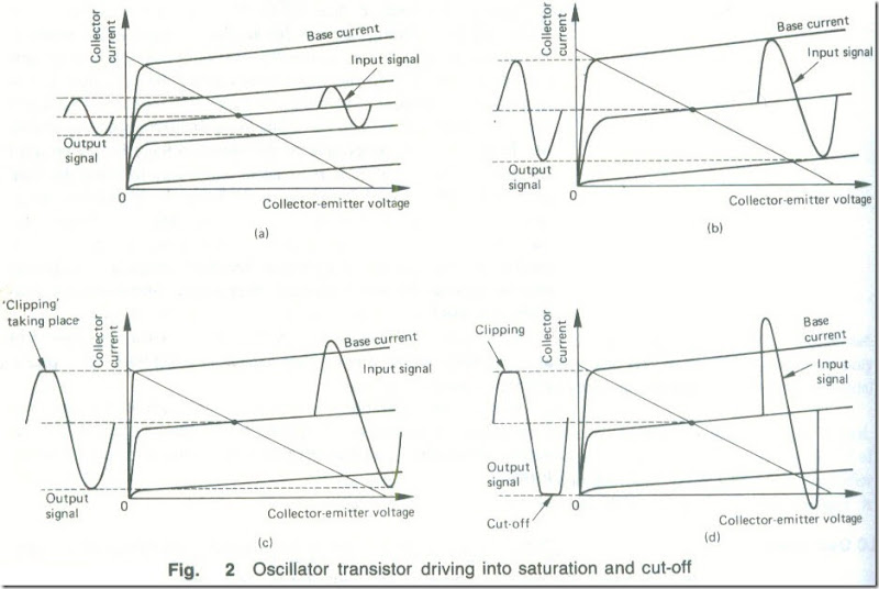
When Class A bias is used the bias and d.c. stabilization circuitry is the same as that for a transistor amplifier. As the amplitude of the signal increases, the operating point of the transistor is varied over a larger part of its output characteristics until the device is driven into saturation on one half-cycle and into cut-off on the other. The gain of the transistor is then reduced to unity as required. The principle is illustrated by the waveforms shown in Fig. 2. In Fig. 2(a) the oscillatory voltage applied to the base of the transistor is small and so the peak base current only varies the collector current by a small amount either side of its quiescent value. With increase in the signal amplitude (Fig. 2(b) the amplitude of the a.c. collector current increases more or less in proportion. With still further increase in the oscillatory base current, the collector current may be varied from approximately zero on one half-cycle to a maximum of Vcc/RL on the other half-cycle. If the input signal amplitude rises still further, one (Fig. 2(c) or both (Fig. 2(d) half-cycles of the collector current may be clipped. In Fig. 2(d) the positive half-cycle is clipped because the transistor has driven into saturation and the negative half-cycle is clipped since the transistor cuts off. The collector current waveform is non-sinusoidal but this does not lead to a distorted output voltage waveform because the collector load consists of a parallel-tuned circuit with enough selectivity to reject all harmonics. The frequency of oscillation is mainly determined by the parallel-tuned circuit and so, to a good approximation, may be taken as being equal to the resonant frequency of the circuit.
Fig. 2 Oscillator transistor driving into saturation and cut-off
Tuned Collector Oscillator
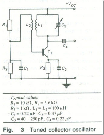
Fig. 3 shows the circuit of a tuned collector oscillator; the frequency-determining tuned circuit is connected in series with the collector terminal of the transistor. R1 , R2 and R3) are bias and d.c . stabilization components while C1 and C2 are decoupling components. Variable capacitor C3 tunes the circuit to oscillate at the desired frequency and C4 is a d.c. blocking component. The action of the circuit is as follows. When the collector supply voltage is first switched on, the resulting surge of d.c. collector current causes a minute oscillatory current to flow in the collector tuned circuit. This current flows in inductor L1, and induces an e.m.f. at the same frequency into inductor L2 . This voltage is then applied to the base of the transistor. The transistor introduces 1800 phase shift between base and collector and hence the mutual inductance coupling between L1 and L2 must be such that the loop phase shift is zero. The amplified voltage causes a larger oscillatory current to flow in L1, and induces a larger e.m.f, into L2 and so on. Provided the loop gain is greater than unity the oscillation amplitude builds up until the point is reached where the transistor is driven into saturation and cut-off during alternate half-cycles of the oscillatory waveform. The loop gain of the circuit is then reduced to unity and the amplitude of the oscillations remains constant. The frequency of oscillation is given by
fosc = 1/[2μ√(L1C1)]
Example 1
A tuned collector oscillator uses an inductance of 60 μH and a variable capacitor to produce oscillations over the frequency band I to 2 MHz. Determine the necessary range of the variable capacitor.
Solution
The maximum capacitance will produce the minimum oscillation frequency of 1 MHz. Hence,
C(max) = 1/(4μ2 X 1 X 1012 X 60 x 10-6) = 422 pF
C(min) = 422/4 = 105.5 pF
Range of variable capacitor = 105 to 422 pF (Ans.)
Hartley Oscillator
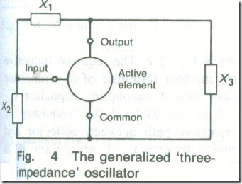
Both the Hartley and Colpitt’s oscillator can be represented by the generalized circuit shown in Fig. 4, in which X1 , is the reactance connected between input and output, and X2 is the reactance between input and common, and X3 is the reactance between output and common. For oscillations to occur, the reactances X2 and X3 must be of the same sign and the reactance X1, must be of the opposite sign. If X2 and X3 are both inductive and X1, is capacitive, a Hartley oscillator is formed; conversely, for a Colpitt’s oscillator, X2 and X3 are capacitive and X1, is inductive.
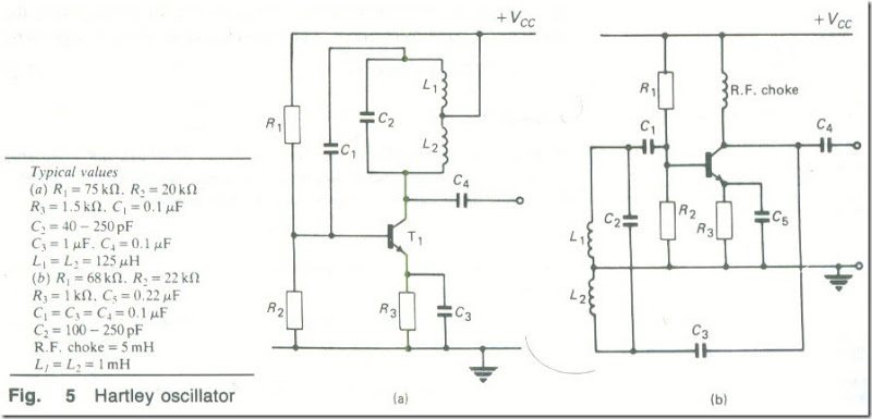
Fig. 5 shows two versions of the Hartley oscillator. In these circuits R1, R2 and R3 provide bias and d.c. stabilization and C1, is a d.c. blocking capacitor having negligible reactance at the oscillation frequency. Comparing Figs. and 5 it can be seen that X1=l/ɷC2, X2=ɷL1, and X3=ɷL2. The frequency of oscillation is given approximately by
fosc = l/{2μ√[C2(L1+ L1)]} (7.3)
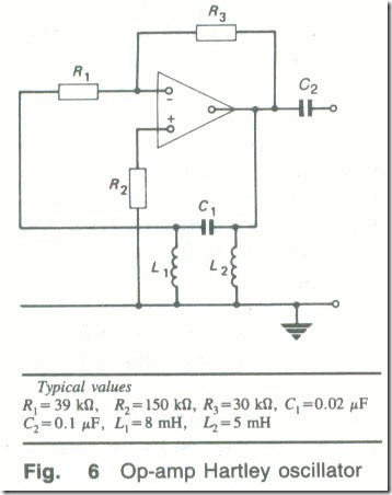
The circuit should have a minimum voltage gain equal to L1/L2. The Hartley oscillator can also be made using an op-amp to provide the necessary gain, and Fig. 6 gives a possible circuit. The frequency of oscillation is given by equation (7.4), i.e.
fosc = 1/{2μ√[C1(L1+ L1)]} (7.4)
Due consideration must of course be given to the bandwidth and slew rate limitations of an op-amp when selecting a .device for the purpose.
The minimum voltage gain necessary to ensure a loop gain of unity is equal to the ratio L1 / L2 and it is obtained by the suitable choice of the resistors R1 and R2 Other factors which must be observed are: (a) R1 should have a resistance that is several times larger than the reactance of L1 ; and (b) the reactance of R1 should be several times larger than the output resistance of the op-amp.
Example 2
Design a Hartley oscillator to operate at a frequency of 4000 Hz. Use a 741 op-amp.
Solution
A 741 has an output resistance of 75 Ω so that the reactance of L2 should be at least 750 Ω. Using this figure, L2 =750/ (2μ x 4000) ≈ 30 mH. LI can be conveniently made the same value.
From equation (7.4), C1=1/(4μ2x40002x60x 10-3)=26 nF. The gain of the amplifier must be greater than L1/L2 or unity to ensure than oscillations will start. Choosing the gain Av(F) to be nominally 3 gives R2 ≈ 3R1. R1≈ 10 X ɷL1 = 10 x 750=7500 Ω and R2 =3 x 7500= 22 500 22 kΩ, nearest preferred value.
Colpitt’s Oscillator
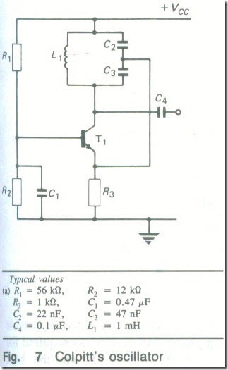
A Colpitt’s oscillator is shown in Fig. 7. The required inductive path between the collector and the base terminals of the transistor is collector, inductor L1 power supply, decoupling capacitor el) and base; the reactance of C1 is negligible at the frequency of oscillation. Similarly, the capacitive path between collector and emitter is via capacitor C3, and the base-emitter capacitive path is C1, power supply and C2 . The frequency of oscillation is approximately given by
fosc = 1/{2μ√[LIC2C3/(C2+C3)]} (7.5)
Example 3
A Colpitt’s oscillator operates at 1.43 MHz. If the inductance LI is
increased by 69% determine the new frequency of oscillation.
Solution
fosc = 1.43 MHz = 1/[2μ√(L1CT)]
fosc = 1/[2μ√(1.69L1CT)]
1.43/ Fosc = √1.69
fosc = 1.43/√ 1.69 = 1.1 MHz (Ans)
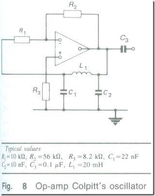
Fig. 8 shows the circuit of a Colpitt’s oscillator that employs an op-amp. As before, the reactive path between the input and the output is of different sign (inductive) to the paths between both input and common, and output and common (both capacitive). The frequency of oscillation is given by
fosc= 1/ {2μ√ [LICI C2/(CI +C2)]) (7.6)
The maximum oscillation frequency will be limited by the bandwidth and slew rate of the op-amp employed. For oscillations to begin the gain of the op-amp must be at least equal to the ratio C2/CI . Also, the reactance of C2 should be a least 10 times larger than the output resistance of the op-amp, and RI should be at least 10 times larger than the reactance of C1 .
Example 4
A Colpitt’s oscillator employs a 741 op-amp set to have a closed-loop gain of 4. The circuit oscillates at 10 kHz with an inductance LI of 30 mH . Calculate the possible values for tuning capacitors C1 and C2 and for the feedback resistors RI and R2.
Solution
The reactance of C2=750 Ω (minimum). Therefore 750= 1/(2μ X 104C2) or C ≏ 21 nF .
The total capacitance
CT = l/(4μ2 X I0 0002x30x 10-3) ≏ 8.44 nF
Hence, 8.44 = 21CI/(21+CI) or C1 = 14 nF.
The ratio C2/C1 = 21/14 = 1.5 = minimum gain.
The reactance of CI = 1/(2μ X 104 X 14 X 10-9) = 1137 Ω.
The input resistor RI should therefore be about II kΩ resistance or more; the nearest preferred value is 12 kΩ, and so R2 = 4 X 12 = 48 kΩ and the nearest preferred value of R2 is 47 kΩ.
RC oscillators
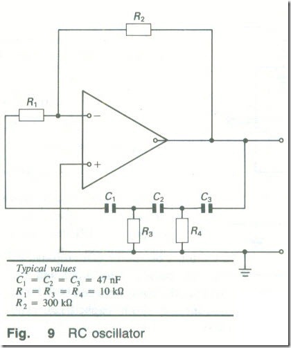
Audio-frequency oscillators most often use a resistance-capacitance network to obtain the loop phase shift of 3600 necessary for oscillations to take place. One type of RC oscillator uses an op-amp and is shown in Fig. 9.
Each of the three RC circuits gives a phase shift of 600 to produce an overall phase shift of 1800 . The op-amp is connected to provide an inverting gain so that the loop phase shift is 3600 as required for oscillations to occur. If, as is usual, R1 = R2 = R3 and the three capacitors are also of equal value, the frequency of oscillation is
fosc = 1/2μ√6CR (7.7)
and the op-amp must have a minimum voltage gain of 29.
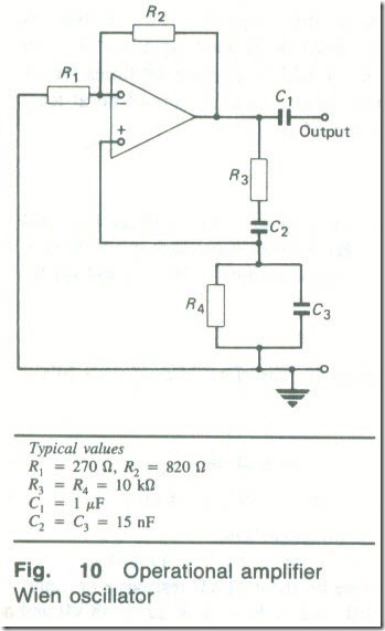
Fig. 10 shows the circuit of an op-amp Wien oscillator. The op-amp introduces a phase shift of 1800 and this means that the RC network must provide a further 1800 for the circuit to function as an oscillator. In the circuit shown the phase-shifting network consists of capacitors C2 and C3 and resistors R3 and R4 . It is usual to make C2=C3 and R3=R4 The closed-loop gain of the op-amp is established by the two feedback resistors R1 and R2 . The output voltage of the op-amp is applied to the RC phase-shifting network, and a fraction β of this voltage is applied to the non-inverting terminal. The series part, R3C2, of the network introduces a phase lead and the parallel part of the network introduces a phase lag. Only at one frequency will the phase lead be equal to the phase lag. Only at this frequency therefore will the voltage applied to the noninverting terminal be in phase with the output voltage. The loop phase shift is then equal to 3600 and the circuit will oscillate provided that the loop gain is greater than unity.
This means that the voltage gain of the op-amp must be greater than the attenuation introduced by the phase-shifting network. At the frequency of oscillation this attenuation is 1/3 so that the minimum gain that the op-amp must provide is 3. The frequency of oscillation is given by
fosc = 1/[2μ√(R3R4C2C3)] (7.8)
If R3=R4 and C2=C3, fosc = 1/2μRC (7.9)
Clearly the oscillation frequency is inversely proportional to the values of resistance and capacitance used in the phase-shifting circuit. For this reason RC oscillators are not used at frequencies much higher than about 1 MHz since stray capacitances would begin to exert a relatively large influence on the frequency of oscillation. A change in frequency requires the simultaneous adjustment of both resistance and capacitance, otherwise the loop gain will alter.
Example 5
The oscillator in Fig. 10 oscillates at 200 Hz. If the three capacitors are all 0.01 μF calculate (a) the resistors R1 and R2, and (b) the percentage error on the frequency of the nearest preferred value is used.
Solution
(a) R = 1/(2μ X 2000 X 0.01 X 10-6) = 7958Ω (Ans.)
(b) The nearest preferred value is 8200 Ω. Using this value
fosc = 1/(2μ X 8200 x0.01 X 10-6) = 1940 Hz
The percentage error is [(1940-2000)/2000] X 100% = -3% (Ans.)
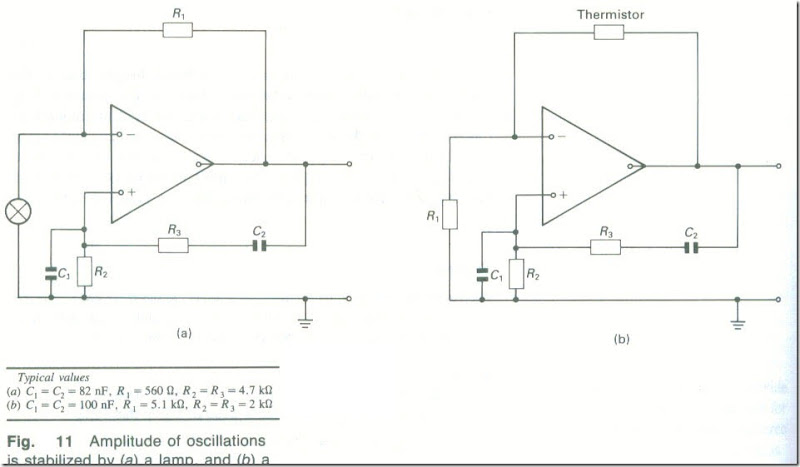
The amplitude of the oscilIatory waveform could be limited by allowing the output transistor to saturate, as is often the practice with an LC oscillator. This would result in a larger percentage harmonic distortion of the output waveform than is normally specified. It is customary, therefore, to employ temperature-dependent negative feedback to provide amplitude stability. This is achieved by replacing the feedback resistor with a negative temperature coefficient (n.t.c.) resistor, such as a thermistor. This is shown by Fig. 11(a). Negative feedback is applied by R and R2 to make the gain of the amplifier equal to (R1+R2)/R1. As the oscillation amplitude increases, the voltage across R2 increases also and so does the power dissipated in the thermistor. The temperature of the thermistor increases and so its resistance decreases. The decrease in the resistance of R2 reduces the gain of the amplifier and hence the output Voltage.
Thermistors are rather expensive devices and, for cheaper amplifier designs, R2 may be a resistor (typically 1 kΩ) and R1 may be a low-current lamp as shown by Fig. 11 (b). The resistance of the lamp will increase with increase in temperature and this will cause the gain to fall.
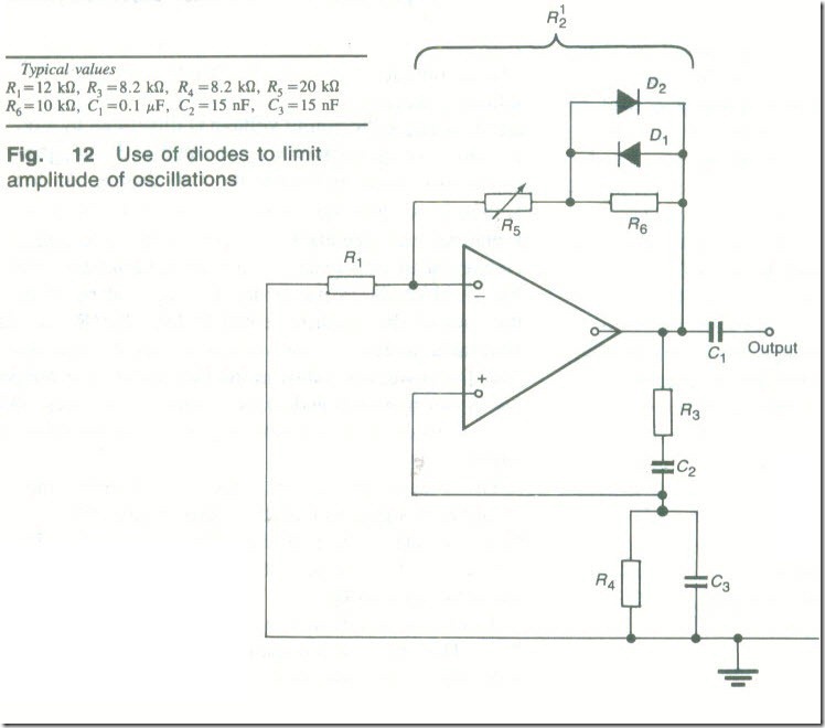
A third method of limiting the output voltage is illustrated by Fig. 12. The effective feedback resistance R21 is equal to Rs in series with the parallel combination of R6 and the two diodes. As the amplitude of the output voltage builds up the point is reached at which the voltage across R6 is large enough to make the diodes conduct on alternate half-cycles. The forward resistance of the turned-on diode shunts R6 to reduce the value of the feedback resistance and hence to reduce the amplifier gain.
The variable resistor R5 is adjusted to give the best amplitude stability. If R5 is too low the oscillations may die away but if it is too high the oscillations will build up until the output waveform is clipped.
Example 6
Design a 6 kHz Wien bridge oscillator that uses an op-amp.
Solution
From equation (7.9)
CR = 1/ɷosc = 1/ (2μ x 6 x 103) = 26.526 X 10⁻⁶ s
A convenient capacitance value is 10 nF and then
R = (26.526 x 10⁻⁶)/(10 x 10-9) = 2652 Ω
= 2700 Ω nearest preferred value (Ans. )
The voltage gain of the amplifier is to be 3 and so R2 = 2 R1 . Convenient values are R1 = 10 kΩ and R2=20 kΩ. R2 can be divided into two 10 kΩ resistors, one fixed and the other variable to allow gain adjustment. Two signal diodes, such as the 1N914, can be employed.

