Small-signal Audio frequency Amplifiers
An amplifier is a circuit that has two input terminals and two output terminals as shown by Fig. 1(a). Very often one input terminal and one output terminal are common, see Fig. 6.1(b). The action of the circuit is to increase the amplitude of, or amplify, the signal applied to the input terminals. In the absence of distortion the input and output signal will have the same waveshape . The voltage gain Av of an amplifier is defined as
Av = Vout/Vin (6.1)
An audio-frequency amplifier is designed to work over a frequency range of about 25 Hz to 20 kHz and its gain should be more or less constant over this bandwidth.
Fig. 1 Principle of an amplifier: (a) separate input and output terminals and (b) one input terminal is common with one output terminal
The requirements for a small-signal amplifier are to:
(a) have a specified voltage gain
(b) provide this voltage gain over a specified bandwidth
(c) have specified constant values of input and output resistance
(d) introduce as little distortion of the signal as possible
(e) work correctly over a range of power supply voltages, particularly for a battery-operated circuit.
A typical specification for an amplifier would be:
voltage gain 200 over a bandwidth of 30 Hz to 15 kHz input resistance 20 kΩ and output resistance 1 kΩ distortion less than 0.1 %.
Principles of Operation
Bipolar transistors and FETs may be used as amplifiers because their output current can be controlled by an a.c. signal applied to their input terminals. If a voltage or power output is required the output current must be passed through a resistive load .A FET has such a high input resistance that its input current is negligible; it can therefore give only a voltage gain. The input resistance of a bipolar transistor depends on the magnitude of the collector current it is passing and it can be made fairly large if the circuit is biased so that the collector current is only a few microamps , By suitable choice of the collector current, and hence of the input resistance, a bipolar transistor may be considered to be either a current-operated or a voltage-operated device.
If the source resistance is much larger than the input resistance of the transistor, the transistor is current operated; if the input resistance is much the larger, it is voltage operated.
Voltage operation of a transistor has the advantage that less noise is introduced. Current operation gives a greater stage gain and, because a larger collector current is employed, a larger maximum permissible output signal. Voltage operation is generally restricted to the input stage of a multi-stage amplifier.
The mutual characteristics of a FET or a bipolar transistor always exhibit some non-linearity, but if a suitable operating point is chosen and the amplitude of the input signal is limited, ‘the operation of the circuit may be taken as linear without the introduction of undue error.
The function of a small-signal amplifier is to supply a current or voltage to a load, the power output being unimportant. In a large signal amplifier, on the other hand, the power output is the important factor and to obtain an adequate power output the output current and voltage swings must cover most of the characteristics.
In modern electronics most amplifiers are either op-amps or IC a.f, power amplifiers.
Choice of Configuration
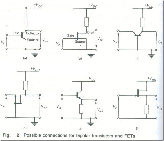
The various ways in which a bipolar transistor or a FET may be connected to provide a gain are shown in Fig 2.
A transistor connected as a common-base amplifier (Fig. 2(c)) has a current gain hfb less than unity (typically about 0.992), a low input resistance of the order of 50 0, and an output resistance of about 1 MΩ. Because the current gain j§ less than unity, common-base stages cannot be connected in cascade unless transformer coupling is used. Audio-frequency transformers, however, have the disadvantages of being relatively costly , bulky and heavy and having a limited frequency response.
The current gain hfe of a transistor connected in the commonemitter configuration (Fig. 2(a)) is much greater than the current gain of the same transistor connected with common base, i.e. hfe = hfb/(1 – hfb)· Coupling of the cascaded stages of a multi-stage amplifier can be achieved without the use of a transformer. Usually, common-emitter stages are biased so that the transistor is current operated. Then the input resistance is in the region of 1000-2000Ω while the output resistance is some 10-30 kΩ.
The common-collector circuit, or emitter follower is shown in Fig. 2(e). This connection has a high input resistance, a low output resistance and a voltage gain of less than unity. The main use of an emitter follower is as a buffer circuit that can be used to connect a high-resistance source to a low-resistance load.
In the normal mode of operation of a FET amplifier (Fig. 2(b)) the source is common to the input and output circuits, the input signal is applied to the gate, and the output is taken from between the drain and earth. This connection provides a voltage gain and it has a high input impedance.
Fig. 2(f) shows the FET equivalent of the emitter follower and it is known as the source follower circuit. Lastly, Fig. 2(d) shows the common-gate connection; this. is not used at audio frequencies.
Most a.f. small-signal amplifiers-employ the bipolar transistor because of its much larger mutual conductance, and hence larger voltage gain.
Choice of Operating Point
The mutual characteristic of a PET with a resistive drain load shows how its drain current varies with change in its gate-source voltage for a particular value of drain supply voltage. Similarly, the mutual characteristic of a bipolar transistor shows how the collector current of the transistor varies with change in the base-emitter voltage for a particular value of collector supply voltage.
A mutual characteristic can be used to determine, graphically, the waveform of the output current for a particular input signal waveform. Ideally, the two waveforms should be identical, but this requires the mutual characteristic to be absolutely linear. In practice, some nonlinearity always exists and, for minimum signal distortion, care must be taken to restrict operation to the most linear part of the characteristic. For this a suitable operating or quiescent point must be selected and the amplitude of the input signal must be limited, so that the operation is kept to the more linear part of the characteristic. The chosen operating point is determined by the application of a steady bias voltage or current. For the maximum signal handling performance the operating point is usually placed in the centre of the linear portion of the mutual characteristic. Then an alternating signal centred on this operating point produces equal swings of output current above and below the quiescent value, as shown in Figs. 3(a) and (b) for a bipolar transistor.
The output current may conveniently be regarded as a direct current having an alternating current superimposed on it. The direct current is equal to the current that flows when the input signal is zero, known as the quiescent current, and the alternating current has a peak-to-peak value of Imax – Imin.
The output current clearly flows at all times during each cycle of the input signal waveform. The active device is said to be operated under Class A conditions. The peak value of the signal waveform should, at all times, be less than the bias voltage, or current, 6therwise the output waveform will be distorted.
Note that Fig. 6.3(b) shows the input current as having a sinusoidal waveform; however, the relationship between the input voltage and the input current of a bipolar transistor is not a linear one unless the steady bias current is much larger than the signal current. This is because the input resistance of a transistor is not a constant quality but varies with change in input voltage.
The selection of the operation point for a Class A amplifier depends on a number of factors:
(a) Maximum output voltage. If the maximum possible output voltage is wanted from a transistor amplifier stage the collector-emitter voltage V CE should be chosen to have a value which is approximately one-half of the collector supply voltage V CC. This choice will position the operating point roughly half-way along the d.c. load line drawn on the output characteristics.
(b) Maximum voltage gain. To obtain the maximum voltage gain the hfe of the transistor should be at, or near, its maximum value. This means that the transistor should be biased to have a particular value of collector current. Also, the collector resistor should be of as high a value as possible.
(c) Minimum noise. When noise is an important consideration the bias point must be such that the collector current is very small.
(d) Battery-operated equipment. When the circuit is a part of a battery-operated equipment a most important consideration will be keeping the current taken from the battery as low as possible. This means that the quiescent collector current should be kept as small as possible. Often the chosen operating point is a compromise between these conflicting factors.
Small-signal a.f. amplifiers always operate under Class A conditions.
Class B and Class C Operation
Class A operation of an amplifier offers low signal distortion. The maximum theoretical efficiency with which the d.c. power taken from the power supply can be converted into a.c. signal power output is, however, only 50%, and practical efficiencies are lower than this. To obtain a greater efficiency than 50%, an amplifier may be operated under either Class B or Class C conditions.
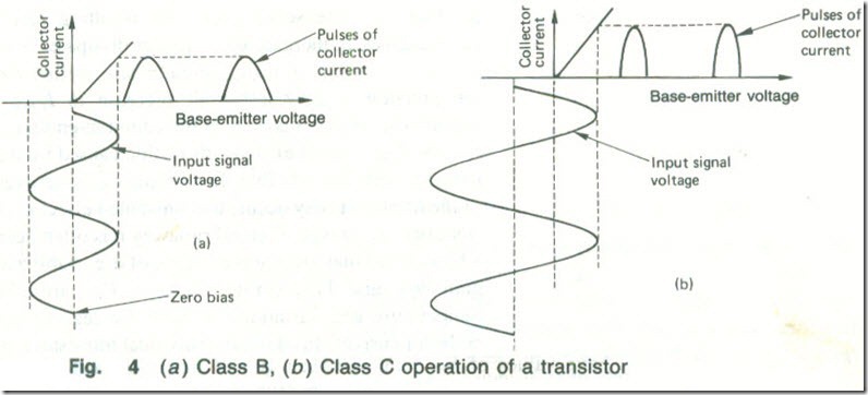
With Class B operation (see Fig .4(a) which refers to a bipolar transistor) the operating point is set at cut-off. The output current flows only during alternate half-cycles of the signal waveform. It is evident that the output current waveform is highly distorted; Class B bias can therefore only be used with circuits that are able to restore the missing half-cycles of the signal waveform. Such circuits are known as push-pull amplifiers and tuned radio-frequency amplifiers. Class B operation has a maximum theoretical efficiency of 78.5%.
Even greater efficiency can be obtained with Class C bias. With Class C bias, shown in Fig. 4(b), the operating point is set well beyond cut-off. The output current flows in the form of a series of narrow pulses having a duration which is less than half the periodic time of the input signal waveform and it is therefore highly distorted.
Class C bias is used with radio-frequency power amplifiers and with some oscillator circuits. These employ a tuned collector load that is able to reject all the unwanted frequencies that are contained in the amplified signal and so restore the original signal waveshape. Class C bias is only used for amplifiers that handle sinusoidal signals.
Another type of operation is known as Class D. In a Class D amplifier the output transistors are operated as switches that are either ON or OFF. The required output voltage is obtained by varying the mark- space ratio of a rectangular wave. The power dissipation of a Class D amplifier is low because the output transistors are either ON or OFF and so the efficiency is very high.


