Multi-stage Amplifiers
Very often the voltage gain that an amplifier is required to provide is greater than can be supplied by a single stage. It is then necessary to connect two, or more, stages in cascade to obtain the required gain The term ‘cascade’ means that the output terminals of one stage are connected to the input terminals of the next stage. The overall voltage gain of a number of cascaded amplifier stages is equal to the product of their individual gains, i.e. G = G1 X G2 X G3 …
Example 15
An amplifier stage has a voltage gain of Av . If two such stages are connected in cascade to obtain an overall voltage gain of 1000, what is the required gain per stage?
Solution
G1 X G2 = G2 = 1000
3√1000 = 31.62 (Ans.)
Exercises
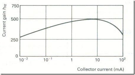
1 – Fig. 37 shows how the d.c. current gain hFE of a transistor varies with the collector current Ie. If the maximum gain is required determine the value of Ic that should be chosen.
2 – List the factors that should be taken into account when choosing a suitable operating point for a transistor.
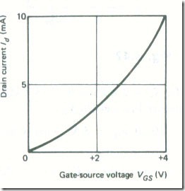
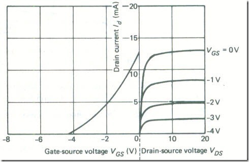
3- The mutual characteristic of an n-channel enhancement-mode MOSFET is shown in Fig. 38. The bias voltage is + 2 V. If a sinusoidal signal of peak value 1V is applied to the device determine the waveform of the drain current.
4- Explain, with the aid of a typical mutual characteristic, why Class B or Class C bias cannot be used with a single-ended resistance-loaded amplifier.
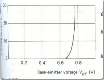
5- Fig. 39 shows a typical mutual characteristic for a bipolar transistor. Determine suitable base-emitter bias voltages for (a) Class A, (b) Class 8 and (c) Class C bias.
6- Explain why d.c. stabilization of a FET is necessary even though thermal runaway is not a problem. Hence, explain the disadvantage of the circuit given by Fig. 40(a).
7- In Fig. 41(a), VDD = 12 V. R3 = 3 kΩ and VDS = 6 V. Calculate the drain current. If R1 = R2 calculate VGS also.
8- In the circuit of Fig. 6.40(b). R1 = 470 kΩ, R3 = 3 kΩ , R3= 1.2 kΩ and VDD = 12 V. Calculate the gate-source bias voltage if the drain current is 1.5mA.
9- In Fig. 40(c), R2 = 150 kΩ. R1= 22 kΩ , R3 = 2 kΩ and R4 = 3.8 kΩ.
If VDD = 15 V and ID = 1.5 mA calculate (a) VDs and (b) VGs.
10- In Fig. 41(b) R1 = 300 kΩ and Rl = 4.7 kΩ. if VDS = 5 V, what is the value of VGS ?
11- In the circuit of Fig. 42. VCC = 6 V and RB = 470 kΩ. If VBE = 0.61 V, calculate the base current IB
12- In Fig. 43 the collector-to-earth voltage is 9 V, RL = 3 kΩ and Ic = 2 mA. Calculate the supply voltage Vcc. If the emitter resistor is I kΩ calculate VE .
13- In Fig. 43 Vcc = 12 V, the collector-to-earth voltage is 6 V and the power dissipated in RL. is 6 mW. Calculate (a) RL and (b) Ic .
14- In Fig. 43 R3 = 1.2 kΩ and IC = 1.8 mA. If hFE= 100 and VBE= 0.62 V calculate (a) IB and (b) the voltage across R2 .
15- The transistor used in the circuit of Fig. 44 has VBE = 0.63 V and hFE = 85. Calculate IC .
16- In Fig. 43 Vcc = 12 V and Ie = 2 mA. If 1/10 th of the supply voltage appears across R3 calculate R3. If VCE = Vcc/2 calculate RL.If hFE = 100
calculate IB If IRl = 10/IB calculate R1 and R2 VBE = 0.65 V.
For the circuit of 6.16. calculate the d.c. input power. Also find the collector dissipation for zero signal conditions.
18- A transistor has hFE = 120 and ICBO = 20 nA. Calculate its collector current when the base current is 20μA.
19- In the circuit of Fig. 43 VCC = 12 V, R1 = 33 KΩ, R2 = 10 kΩ and R3 = 1.2 kΩ. If Ic = 1.75 mA calculate the VBE bias voltage of the transistor.
20- The bias circuit of Fig. 20 is designed with the hf£ value assumed to be the nominal value of 100. One circuit is constructed using this type of transistor where the hFE value is the minimum of 70. Explain how the circuit operates to ensure that the collector current is very nearly equal to the designed-for value.
21- The signal voltage applied to the base of a transistor with gm = 40 mS has a peak value of 0.1 V. Calculate the peak value of the a.c. component of the collector current. If the collector load resistance is 4.7 kΩ determine the output voltage of the circuit and the voltage gain.
22- An audio-frequency amplifier uses a FET with rds = 10 kΩ and gm = 5 mS.
What value of drain load resistor is needed to give a voltage gain of 40 ?
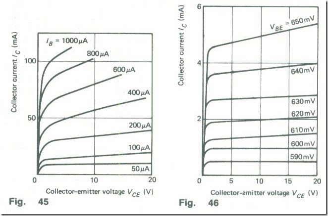
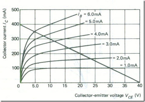
23- On the output characteristics given in Fig. 45 draw the load line for a d.c. load of 400 ohms. The operating point is IB = 150 μA and the supply voltage is 20 V. If the emitter resistance is 100 ohms calculate VE, VCE and the collector-to-earth voltage. Determine the peak-to-peak output voltage when a sinusoidal voltage varies the base current by ± 50μA.
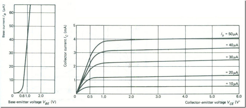
24- Fig. 46 shows the collector current of a transistor plotted against collectoremitter voltage for various values of base-emitter voltage. The transistor is used in an amplifier (Fig. 43) with Vcc = 20 V, RL = 3.5 kΩ and R3 = 500 Ω . Draw the load line and choose a suitable operating point to give the maximum possible output voltage. Determine the peak-to-peak collector current when the peak base voltage change is 25 mV. Calculate the voltage gain of the circuit (a) from the load line. and (b) using the expression Av = gmRL .
25- Figs 47(a) and (b) show. respectively. the input and output characteristics of a transistor. The transistor is used in a single-stage amplifier with Vcc = 6 V, RL = 1800 ohms and emitter resistance is 200 ohms. Draw the load line and mark the operating point for a base bias current of 20 μA. Determine the required bias voltage VBE Calculate the ratio δIC/δVBE
26- Fig. 48 shows both the mutual and drain characteristics of an n-channel JFET. If VDD = 20 V draw the load line for RL = 2000 ohms on the drain characteristic and select the operating point VGS = – 2 V. A signal voltage varies VGS between the limits – 1 V and – 3 V. Determine from both sets of characteristics the mutual conductance of the device. Calculate the voltage gain (a) from the load line and (b) using the expression Av = gmRL
27- Fig. 49 shows a transistor output characteristic with a load line drawn on it. Determine the load to which this relates. Caculate the maximum peak-to-peak output voltage and current if the operating point is (a) IB = 1 mA. (b) I, = 3 mA and (c) I, = 5 mA. Comment on the results.
28- For Fig. 49 calculate the d.c. power taken from the supply and the collector dissipation under no-signal conditions. Assume the base-bias current IB to be 3 mA.

