Determination of Gain using a Load Line
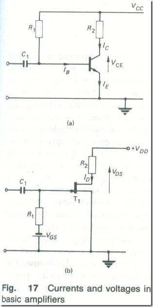
The voltage gain of a FET amplifier or the current gain of a bipolar transistor amplifier can be determined with the aid of a load line drawn on the output current-output voltage characteristics of the device. The currents and voltages existing in the collector or drain circuit of a simple resistance-loaded amplifier are shown in Figs. 17(a ) and (b) respectively. In each of these circuits the d.c. collector or drain current flows in the load resistor R2 and develops a voltage across it. The direct voltage which is applied across the transistor or FET is equal to the supply voltage minus the d.c. load voltage.
Thus, referring to Fig 17
VCE = VCC – lCR2 (6.7)
VDS = VDD – IDR2 (6.8)
Equations (6.6) and (6.7) are of the form y = mx + c and are therefore equations of a straight line. In order to draw a straight line it is only necessary to plot two points; these points can best be determined in the following manner. Point A: Let IC = ID = 0 in equations (6.7) and (6.8) respectively, then
VCE = VCC and VDS = VDD
Point B: Let VCE = VDS = 0 equations (6.7) and (6.8) respectively, then
0 = VCC – ICR2 or IC = VCC/R2
0 = VDD – IDR2 or ID = VDD/R2
If the points A and B are marked on the characteristics and then joined together by a straight line, the line drawn is the load line for the particular values of load resistance and supply voltage. The load line can be used to determine the values of current and voltage in the output circuit, since the ordinate of the point of intersection of the load line and a given input current or voltage curve gives the output current or voltage for that input signal.
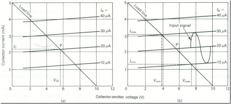
Consider for example, the output characteristics of an n-p-n transistor given in Figs.18(a) and (b), and suppose the transistor is to be used in an amplifier with a collector load resistance of 2000 Ω and a collector supply voltage of 10 V. The two points, A and B, that locate the ends of the load line are at IC = 0, VCE = VCC = 10 V, and at VCE = 0 , IC = VCC/R2 = 10/2000 = 5 mA. These points have been located on the characteristics and the load line drawn between them. The operating point is often chosen to lie approximately in the middle of the load line, and here it has been selected as the point marked P. The required base bias current is then equal to 20 p.A. The d.c. collector-emitter voltage (VCE = VCC – lCR2) is found by projecting vertically downwards from the operating point to the voltage axis. This step is shown by a dashed line in Fig. 18(a) and it determines the standing (or quiescent) collector-emitter voltage as 5.6 V. Similarly, the d.c. collector current which flows is found by projecting horizontally from the operating point towards the current axis. Thus, the d.c. collector current is equal to 2.2 mA.
The d.c. power taken from the collector supply is given by the product of the collector supply voltage and the d.c. collector current, i.e. 10 X 2.2 X 10-3 = 22 mW. The d.c. power Pc dissipated at the collector of the transistor is the difference between the d.c. power supplied to the circuit and the d.c. power dissipated in the load resistance. Hence
PC = 22 X 10-3 – [(2.2 X 10⁻³)2 X 2000] = 12.32 mW Pc is also equal to the product of the d.c. collector current and the quiescent collector-emitter voltage; thus
PC = 2.2 X 10-3 X 5.6 = 12.32 mW
The load line can also be used to find the variations in both the collector current and the collector-emitter voltage which are produced by the application of a signal to the base of the transistor. Suppose
as shown by Fig. 6. 18(b ) that a sinusoidal signal of peak value 10 p.A is applied to the transistor. This signal is superimposed on the base bias current of 20 p.A and so the base current is varied from a minimum value of 10 p.A to a maximum value of 30 p.A. The corresponding values of the collector current and the collector-emitter voltage are determined by projecting to the current and voltage axes from the points of intersection of the load line and the curves for IB = 10 p.A and IB = 30 p.A. This has been shown by the dashed lines drawn on Fig 18(b). The collector current is varied from a minimum value IC(min) = 1.3 mA to a maximum value lC(max) = 3.25 mA. The collector-emitter voltage is varied from a minimum value VCE(min) = 3.6 V to a maximum value VCE(max) = 7.3 V. The a.c. component of the collector current has a peak-to-peak value of (3.25 – 1.3) mA or 1.95 mA, while the peak-to-peak value of the a.c. component of the collector-emitter voltage is (7.3 – 3.6) or 3.7 V .
The current gain Ai of the amplifier is
Hence
Ai = (1.95 x 10⁻³)/(20 x 10-6) = 97.5
Example 7
The transistor used in a single-stage audio-frequency amplifier with a resistance load of 2000 Ω has the data given in Table 2.
Plot the output characteristics of the transistor and draw the load line assuming a collector supply voltage VCC of 8 V.
(i) Select a suitable operating point.
(ii) Determine the current gain Ai when an input signal producing a base current swing of 5 μA about the chosen bias current is applied to the circuit.
(iii) Assuming the input resistance of the transistor is 1900 (1 determine the voltage gain Av.
(iv) Calculate the power gain Ap .
Table 2
|
lc(mA) |
||||||||
|
VCE(V) |
IB = 5μA |
|
– |
IB =10μA |
IB = 15 μA |
IB = 20 μA |
||
|
2 |
0.85 |
1.55 |
2.32 |
3.08 |
||||
|
4 |
1.00 |
1.74 |
2.56 |
3.35 |
||||
|
6 |
1.13 |
1.92 |
2.76 |
3.60 |
||||
|
8 |
1.30 |
2.13 |
3.00 |
3.85 |
Solution
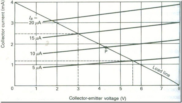
The output characteristics are shown plotted in Fig. 19. The d.c. load line must be drawn between the points
IC = 0, VCE = VCC = 8 V, and
VCE = 0, IC = VCC/R2 = 8/2000 = 4 mA
(i) Since the input signal has a peak value of ± 5 p.A a suitable base bias current is 10 p.A, the operating point is then P.
(ii) When a signal of ± 5 p.A peak is applied to the transistor, the base current varies between 5 p.A and 15 p.A. Projection from the intersection of the load line and the 5 p.A and 15 p.A base current curves to the current axes gives the resulting values of collector current as 1.15 rnA and 2.45 rnA.
The peak-peak collector current swing is therefore 2.45 – 1.15 or 1.30 mA and the current gain is
Ai = (1.3 x 10⁻³)/(10 x 10-6) = 130 (Ans.)
(iii) If the input resistance of the transistor is 1900 n the a.c. voltage applied to the transistor must be
± 5 x 10-6 x 1900 or ± 9.5 x 10⁻³ V
Projecting from the intersection of the load line and the appropriate base current curves to the voltage axis gives the peak-peak collector Voltage as
5.7 – 3.08 = 2.62 V
Voltage gain Av = 2.62/(19 x 10-3) = 138 (Ans.)
Alternatively, using equation (3.7)
Av = AiRL/Rin = (130 x 2000)/1900 = 137 (Ans.)
(iv) The power output of the transistor is the product of the r.m.s. values of the a.c. components of the collector current and the collector-emitter voltage. Therefore
Output power = (peak-peak Ic)/2√2 x (peak-peak Vce)I2√2
= [(IC(max) – IC(min))]/8
= (1.3 X to-3 X 2.62)/8 = 4.258 x 10⁻⁴ W (Ans.)
The input power delivered to the transistor is
I2b(rms)hie = [(5 X 10⁻⁶)/√2]2 X 1900 = 23.75 X 10⁻⁹ W
Power gain Ap = Pout/Pin = 4.258 X 10⁻⁴/23.75 X 10-9 = 17928 (Ans.)
Alternatively, using equation (3.8),
Ap = A2iRL/Rin = AiAv = 130 x 137 = 17810 (Ans.)
Example 8
Determine the mutual conductance of the transistor in Example 4. Use this value to calculate the voltage gain of the circuit.
Solution
gm = hfe/hie = 130/1900 = 68.4 mS (Ans.)
or, gm = 38 X 10-3 X IC = 38 X 10-3 X 1.8 = 68.4 mS (Ans.)
Voltage gain = gmRL = 68.4 X 10-3 X 2 X 103 = l37 (Ans.)
Since the mutual conductance 8m is primarily determined by the d.c. collector current its value is more predictable than is the value of hfe and so gm is increasingly employed in performance calculations.
Example 9
The bipolar transistor used in an audio-frequency amplifier has hie = 250 and Rin = 1500 Ω . (a) Calculate the collector load resistance needed to give a voltage gain of 200. (b) A voltage source of e.m. f. 20 m V and internal resistance 600 n is connected to the input terminals of the amplifier. Calculate the output voltage.
Solution
(a) 200 = 250RL/1500, RL = (200 X 1500)/250 = 1200 Ω (Ans.)
(b) Vin = (20 X 15(0)(600 + 1500) = 14.29mV
Vout = 200 X 14.29 X 10-3 = 2.86 V (Ans.)
A.C. Load Lines
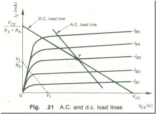
Very often the load into which a transistor or a FET works is not the same for both a.c. and d.c. conditions. When this is the case two load lines must be drawn on the characteristics: a d.c. load line to determine the operating point, and an a.c. load line to determine the current or voltage gain of the circuit. The a.c. load line must pass through the operating point.
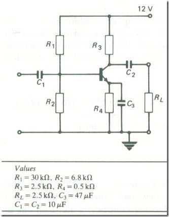
Fig.20 shows the circuit of a single-stage common-emitter amplifier using potential-divider bias. The emitter decoupling capacitor C3 has a very high reactance at very low frequencies and does not shunt the emitter resistance R4 at zero frequency (direct current). The d.c. load on the transistor is therefore R3 + R4 ohms. At signal frequencies the reactance of C3 is low and the a.c. load on the transistor is reduced to R3 ohms. A d.c. load line is first drawn on the output characteristics between the points
Ic = 0, VCE = VCC, and
VCE = 0, Ic= VCC/(R3 + R4)
as shown by Fig. 21. A suitable operating point P is then selected .
The a.c. load line must be drawn passing through the operating pour with a slope equal 10 the reciprocal of the a.c. load resistance on the transistor, i.e. a slope of – 1/R3. To avoid extending the current axis, proceed as follows. (a) Assume that the a.c. load is actually a d.c. load, and using any convenient value of supply voltage (V1 in Fig 21), draw lightly me corresponding d.c. load line using the method previously explained, i.e. draw the line between the points V1 and V1/R3· (b) This load line has the required slope, so now draw the actual a.c. load line parallel to it and passing through the operating point.
Another instance where the a.c. load on a transistor is different from the d.c. load is shown by Fig. 22. The external load resistance RL, which may be me input resistance of a following amplifier stage, is coupled to the transistor by the coupling capacitor C2. If the decoupling capacitor C3 has negligible reactance at all signal frequencies the d.c. load on the transistor is R3 + R4 ohms and the a.c. load is R3 in parallel with RL, i.e.
RL(eff) = R3RL/(R3 + RL
Example 10
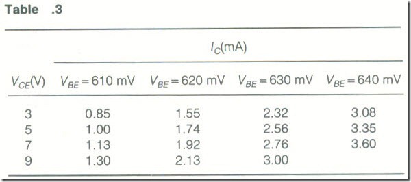
The bipolar transistor used in the circuit of Fig. 22 has the data given in Table 3. Plot the output characteristics of the transistor, draw the d.c.load line and select a suitable operating point. Draw the a.c. load line and use it to find the a.c. voltage across the 2500 Ω load RL when an input signal Vbe of peak value 15 mV is applied to the circuit. Assume all the capacitors have zero reactance at signal frequencies.
Solution
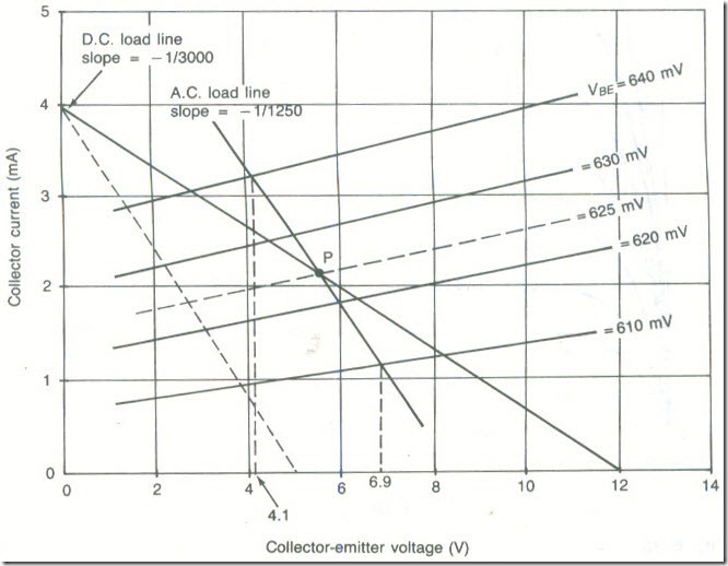
The output characteristics are shown plotted in Fig. 23. The d.c. load on the transistor is R3 + R4 3000 Ω: the d.c. load line must therefore be drawn between the points
Ic= 0, VCE = 12 V and
VCE = 0, Ic = 12/3000 = 4 mA
Since the input signal has a peak value of 15 mV, a suitable base bias voltage is 625 mV, the operating point is then P.
The a.c. load on the transistor is the 2500 Ω collector resistor in parallel with the 2500 0 load, i.e. 1250 O. An a.c. load line with a slope of -1/1250
must therefore be drawn on the output characteristics. To draw a d.c. load line with the same slope assume a convenient supply voltage. say S Y: then this d.c. load line joins the points
VCE= 5 V and lc = 5/1250 = 4mA
The equivalent e.c. load line is shown dotted and the wanted a.c. load line has been drawn parallel to it and passing through the operating point.
When a signal of ± 15 mV (peak) is applied 10 the transistor VBE varies between 610 mV and 640 mV. Projection from the intersection of the load line and the 610 mV and 640 mV VBE: curves gives the resulting values of collector voltage as 4.1 V and 6.9 V. The peak collector signal voltage is therefore (6.9 – 4.1)/2 or 1.4 V.
Voltage Gain of FET Amplifier
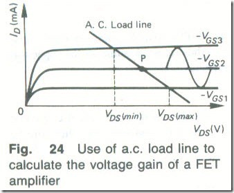
Fig. 24 calculate the voltage gain of a FET amplifier
The voltage gain of a FET amplifier can also be found with the aid of a load line. For example, Fig. 24 shows an a.c. load line drawn on the drain characteristics of a FET. and the dotted projections from the load line show how the drain voltage swing, resulting from the application of an input signal voltage. can be found. The voltage gain Av of the FET amplifier is
Example 11
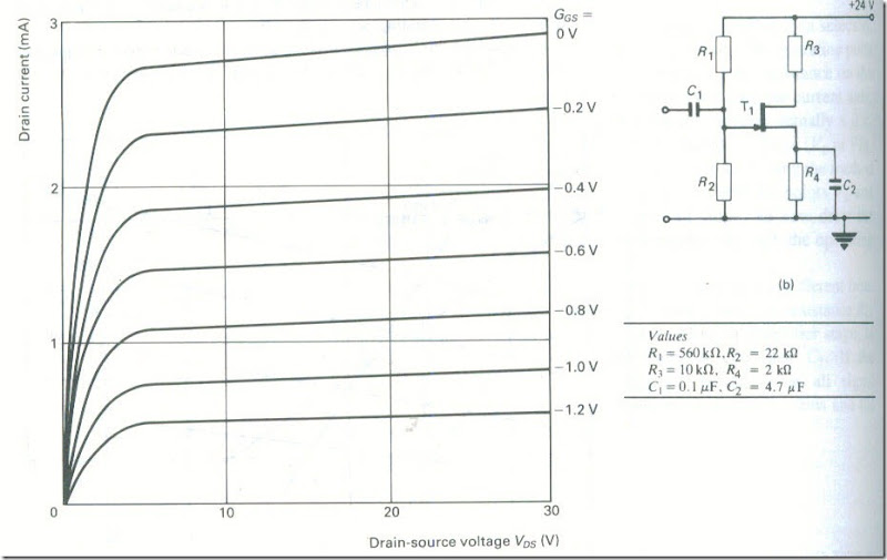
Fig. 25(a) shows the drain characteristics of a common-source n-channel lFET, which is used in the single-stage amplifier circuit shown in Fig. 25(b). Draw the d.c. load line and select a suitable operating point. Draw the a.c. load line and use it to find the voltage gain when a sinusoidal input signal or 0.3 v peak is applied.
Solution
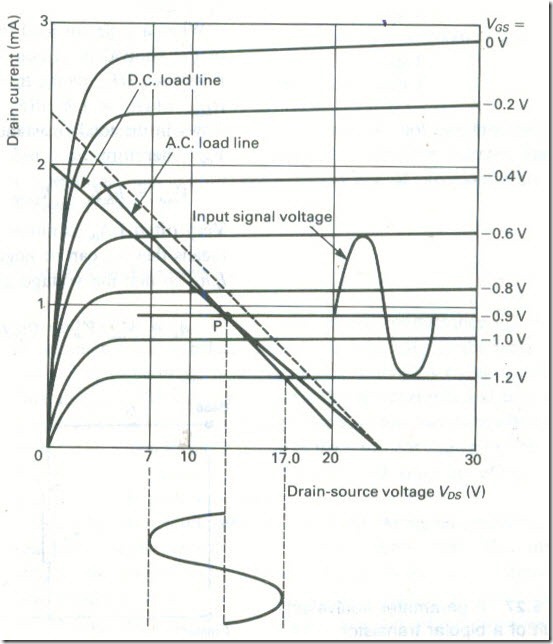
The d.c. load on the FET is 12 kΩ, and hence the d.c. load line must join the points
ID = 0 VDS = 24 V and
VDS = 0, ID = VDD/(R3 + R4) = 24/(12 x 103) = 2 mA
The load line has been drawn in Fig. 26. A suitable operating point is VGS = -0.9 V. The a.c. load line must pass through the chosen operating point
with a slope of -1/(10 x l03 ) and it has been drawn parallel to the dotted line joining the points
ID =0, VDS = 24 V and VDS =0, ID = 24/(10 X 103) = 2.4mA.
From the a.c. load line, the voltage gain of the circuit is
Av = (17 – 7)/( -1.2 – (-0.6» = -16.7 (Ans.)

