Sequential Digital Circuits flip-flop
A sequential logic circuit is one that is able to store one bit, or more, of data and whose output depends on both stored data and new input data.
The basic sequential logic circuit is the flip-flop. A flip-flop is a circuit which has two stable states: either it is SET, i.e. its Q output is at logical I, or it is RESET, i.e. its Q output is at logical 0. There are four kinds of flip-flop in use; these are known as the S-R, the J ̶ K, the D, and the T flip-flops. A flip-flop may be used on its own in a circuit, when it is used as a 1-bit store, or it may be used in conjunction with one or more other flip-flops to form a counter or a shift register.
The S-R Flip-flop
The S-R flip-flop is a circuit that has two input terminals S and R, and two output terminals Q and Q. In addition, an S—R flip-flop may be clocked; this means that a rectangular pulse waveform, known as the clock, is applied to a third input terminal to determine the times at which the circuit changes state. The symbol for an unclocked S ̶ R nip-flop is shown by Fig 1.
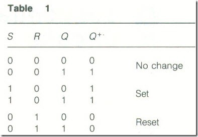
The truth table of an S-R flip-flop is given by Table 9.1, In this table Q is the present state of the Q output terminal and Q+ is the next state. At all times the Q terminal is complementary to the Q terminal, i.e. if Q = 1 then Ǭ = 0.
(a) When both the S and R input terminals are at the logical 0 level the flip-flop will remain in its present state, i.e. Q+ = Q
(b) When S=1 and R = 0 the next state of the circuit will be Q = 1 , Ǭ = 0 , whatever the present state. The flip-flop is said to be SET.
(c) When S = 0 and R = 1. the next state of the circuit will be Q = 0 , Ǭ = 1, whatever the present state. The circuit is said to be RESET.
(d) When both the S and the R inputs are at 1 the flip-flop may, or may not, change states. The next state is not predictable and is said to be indeterminate. Such a condition cannot be tolerated in a practical system and if there is a possibility of the state S = R =1 arising then the S ̶ R flip-flop should not be used.
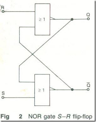
The S ̶ R flip-flop can be obtained as an integrated circuit, e.g. TTL 7471 and CMOS 4043, but it can also be made using either NAND or NOR gates. Fig .2 shows how two NOR gates can be interconnected to produce an S ̶ R flip-flop.
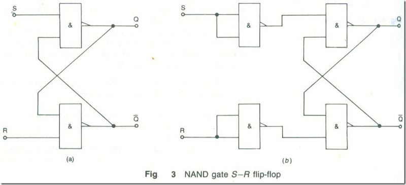
If two NAND gates are similarly connected, as in Fig .3{a), the truth table has the ‘no-change’ and ‘indeterminate’ states interchanged. To obtain the true S—R flip-flop logical operation two further NAND gates are needed, connected as shown by Fig .3(b).
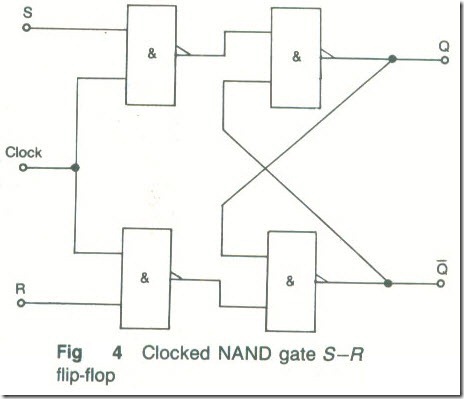
Often it is desirable that the switching of the flip-flop occurs at defined instants in time that are specified by the clock (the clock is a rectangular pulse waveform). The NAND S-R flip-flop is easily modified to give clocked operation as shown by Fig .4. Whenever the clock is at logical 0 the outputs of both of the input NAND gates must be at 1 regardless of the logical states of the S and R inputs. The circuit will then be unable to change state. Only when the clock input is at logical 1 will the S and R inputs control the operation of the circuit.
The J-K Flip-Hop
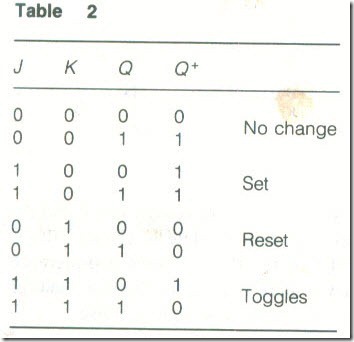
The J-K flip-flop has a truth table which differs from that of the No change S-R flip-flop only in that the unwanted indeterminate state does not exist. The truth table of a J-K flip-flop is given by Table .2. It should be noted that when S = R – 1 the circuit always changes
state or toggles.
A J-K flip-flop can be made by modifying the circuit of Fig .4 but the resulting circuit is subject to unwanted hazards. Instead, one of the many integrated circuit J-K flip-flops is generally employed.
Integrated J ̶ K flip-flops are either master— slave or edge-triggered devices. The block diagram of a master-slave J-K flip-flop is shown
in Fig .5. The master flip-flop is directly driven by the clock but the slave flip-flop is driven by the clock pulses after they have been inverted. When the clock is HIGH the inverted clock is LOW and this isolates (he slave from the master. Both die flip-flops are triggered by the leading edge of a clock pulse. The master flip-flop responds to the data present al its J and K terminals as soon as die leading edge of a clock pulse arrives. The output of die master is then set, or reset, in accordance with the input data; the slave flip-flop does not respond to this because the clock at its clock input is at its trailing edge. When the trailing edge of the clock pulse occurs the inverted clock is at its leading edge and goes HIGH; at this point die data stored by die master is transferred to the slave flip-flop and appears at the output terminals Q and Ǭ of the circuit. This means that the output state of a master-slave J—K flip-flop changes at the trailing edge of the clock pulse. The J and K inputs must not change state while the clock remains HIGH.
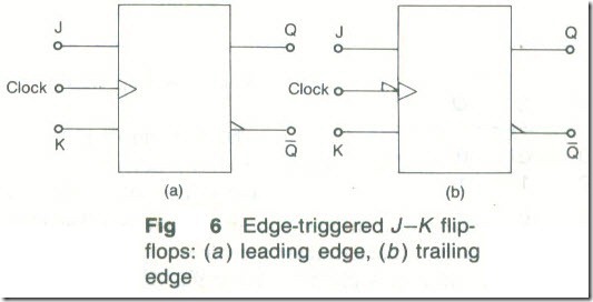
Most IC J-K flip-flops are edge-triggered. This means that they change state, as determined by the J and K inputs, either as the clock changes from 1 to 0 — a trailing-edge-triggered device — or as the clock changes from 0 to 1 — a leading-edge-triggered device. Leading-edge triggering is indicated by a wedge on the clock input of die flip-flop symbol, Fig .6(a). Trailing-edge triggering is indicated by the addition of a small triangle, Fig .6(b).
The operation of die edge-triggered circuit is very quick and the J and K inputs do not need to be held constant while the clock is HIGH. For this reason edge-triggered J—K flip-flops are used in preference to master-slave types whenever there is a chance that the J and/or K inputs may change during the duration of a clock pulse.
Preset and Clear
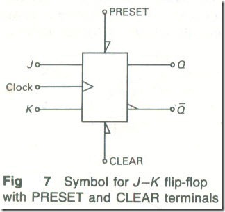
Some J-K flip-flops can be set or reset (cleared) by the application of die logic 0 voltage level (o its PRESET, or its CLEAR, terminal respectively. The terminals are said to be active LOW. Fig. 9.7 shows me symbol for a leading-edge-triggered J-K flip-flop with PRESET and CLEAR terminals. The flip-flop is set, or is cleared, immediately the appropriate terminal is taken LOW regardless of the state of the clock input. The reset and clear actions are hence non-synchronous.
The D flip-flop
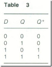
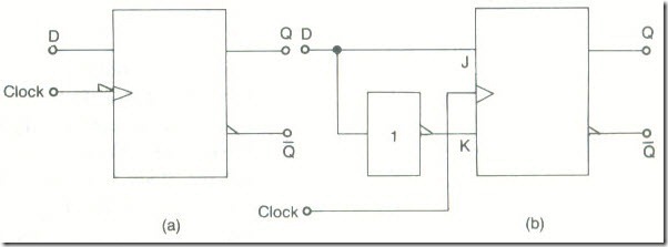
The D flip-flop has one input terminal, a clock terminal and two output terminals, see Fig .8(a). The truth table of a D flip-flop is given by Table .3. Clearly, the Q output always takes up the logical state of the D input. The D flip-flop is readily available in both the TTL and the CMOS logic families but it can also be obtained by modifying a J-K (or S-R) flip-flop in the manner shown by Fig .8(b).
The T Flip-flop
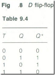
The truth table of a T flip-flop is given by Table .4. It can be seen that every time there is a pulse at the r input the circuit toggles. The r flip-flop is not available as a separate integrated circuit: when one is wanted it is easily made by merely connecting together the J and K inputs of a J-K flip-flop. This is shown by Fig .9.
A counter is digital circuit that is able to count the number of pulses that are applied to its input terminals. It generates binary numbers in a specified count sequence. A counter goes through the specified sequence of numbers when it is triggered by an input pulse waveform and it advances from one number to the next only when a pulse arrives. The counter will go through the same sequence continuously as long as there is an input pulse waveform applied to its clock terminal. A counter consists of a number n of flip-flops connected together so that the output of one is applied to the input of the next. The number of states that a counter can take up is equal to 2" and the highest number which can be stored is 2n -1. A three-stage counter, for example, can have 23 or 8 different stales and a maximum count of 7.
The number of different states is known as the modulus of the counter. A counter may be either synchronous (i.e. its operation is synchronized to the clock) or non-synchronous. The two most common counters are the decade counter and the binary counter. The decade counter has a count of 10; the binary counter has a count of 16.


