Design
Many digital circuits consist of a number of gates which have been interconnected to perform a wanted logical function. The design of a combinational logic circuit starts with the truth table which describes the required logical operation. Once the truth table has been written down it can be used to derive the Boolean expression which describes the circuit. The expression should contain one term for each column (or row) in the truth table for which the output F of the circuit is at the logical 1 state. The expression so obtained should then be simplified, or minimized, if possible to eliminate all unnecessary terms. This step ensures that the final circuit contains the minimum number of gates. Next, the designed circuit is usually converted into an equivalent circuit that uses either NAND or NOR gates only. Besides very often reducing the number of integrated circuits required, the use of just one kind of gate makes both manufacture and fault-finding somewhat easier.
Except for the most simple problems the Boolean equation will not be in its most simplified form. Usually, it will contain a number of redundant terms and so it is often necessary to first simplify each derived Boolean equation. There are two main ways in which Boolean equations can be reduced to their most simple form: one is an algebraic method which relies on a number of Boolean laws and identities; the other uses a mapping technique known as a Karnaugh map.
Boolean Laws and Identities
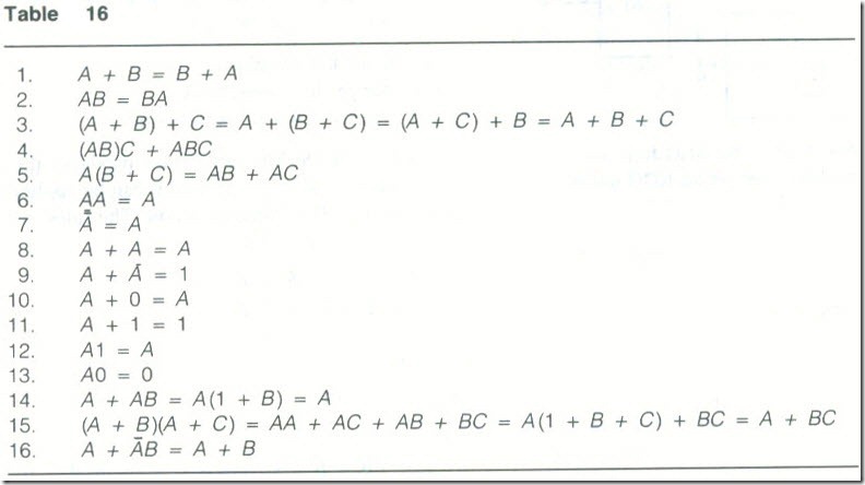
The more commonly used Boolean laws and identities are listed in Table .16. Each of these laws and identities can be proved by writing down the various combinations of A, B and C in a truth table.
Example 4
Use the Boolean identities given in Table .16 to simplify each of the following Boolean equations.
Solution
There are also several other identities that, although sometimes useful, are not essential to know, plus two very important rules that are known as De Morgan’s Rules.
De Morgan’s Rules
The two rules attributed to De Morgan are
ABoth of these rules have already been arrived at by the use of truth tables, see Tables 11 and 13. The rules governing the application of De Morgan’s theorems are:
(a) invert the variables
(b) change the connections
(c) invert the whole expression.
Since either of De Morgan’s rules produces the equivalent of any expression to which it is applied it can be applied to any part of. or the whole of, a Boolean expression. The rules still apply when there are three variables. Thus:
The Use of NAND and NOR Gates to Generate the AND and OR Logical Functions
It is common practice to use either NAND or NOR gates only in a combinational logic circuit. The use of both types of gate to generate the NOT function and of two NAND gales to generate the AND function, or two NOR gates to give the OK function is described on page 175. The use of De Morgan’s rules shows that it is also possible to produce the AND function using NOR gates only and the OR function using only NAND gates.
One rule is ![]() and hence
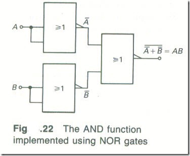
and hence ![]() Fig . 22 shows that this equation can be implemented using three NOR gates.
Fig . 22 shows that this equation can be implemented using three NOR gates.
The other rule is ![]() and hence
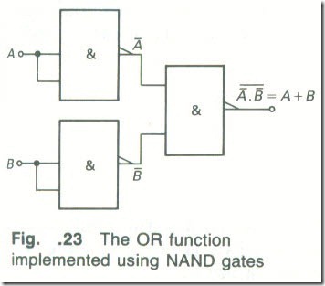
and hence ![]() , and this can easily be implemented using three NAND gates as shown by Fig . 23.
, and this can easily be implemented using three NAND gates as shown by Fig . 23.
In both cases the concept can be extended to three or more input variables.


