Integrated Circuits
The methods used to fabricate silicon planar bipolar and field-effect transistors can be extended to allow a complete circuit to be manufactured in a single silicon chip. All the components, active and passive, which are required by the circuit are formed at the same time in a small piece of silicon, known as a chip. The circuit is known as a monolithic integrated circuit or 1C because only one silicon chip is used. The use of monolithic integrated circuits has a number of advantages over the use of discrete circuits: greatly reduced size and weight; lower costs; complex circuit functions are economically possible, e.g. pocket calculators; and greater reliability. The size and weight reductions occur because a quite complex circuit can be enclosed within a volume of comparable dimensions to those of a single transistor. The cost of an integrated circuit depends on its complexity and the quantity manufactured, but in many cases the cost is no greater than that of one transistor.
Other types of integrated circuit, known as thin-film and thick-film circuits, are also available; with born thin-film and thick-film circuits, resistors and capacitors are fabricated by forming a suitable film on to die surface of a glass or a ceramic substrate. The components are interconnected in the required mariner by means of a deposited metallic pattern. Thin-film components are produced by vacuum deposition of a suitable material on to the surface of the substrate. Thick-film components are produced by painting die substrate with special kinds of ink. Active components and inductors cannot be produced in this way and any such components that are necessary must be provided in discrete form, and be joined into the metallic pattern at the appropriate points. Thick- and thin-film circuits are not used to anywhere near the same extent as monolithic circuits and they will not be discussed in this book.
Integrated Circuit Components
The fabrication of an integrated circuit component is achieved by a sequential series of oxidizing, etching and diffusion. The components that can be formed by this process are transistors (both bipolar and field-effect), diodes, resistors and capacitors; inductors cannot be produced.
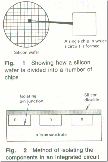
A thin wafer, about 5-10 mils ( One mil is one thousandth of an inch) thick, is sliced from a rod of p-type silicon and will have a surface area of about 4 in2. Since integrated circuit may only occupy an area of about 30 mils2, several thousands of identical circuits can be simultaneously fabricated in the one wafer. The principle is illustrated by Fig. 1, although to simplify the drawing fewer chips have been shown.
Each individual silicon chip acts as a substrate into which the various components making up the circuit can be formed. The components are simultaneously formed by the diffusion of impurity elements into selected parts of the chip.
Since the p-type silicon substrate is an electrical conductor it is necessary to arrange that each of the components is insulated from the substrate. If this is not done the various components will all he coupled together by the substrate resistance. There are a number of different ways in which the required isolation can be obtained, but the most common method utilizes the high-resistance property of a reverse-biased p-n junction (see Fig. 2). Several n-type regions, equal in number to the number of components in the circuit, arc diffused into the p-type substrate. Each of the n-type regions will be isolated from the substrate if the junction is maintained in the reverse-bias condition by connecting the substrate to a potential which is more negative than any other part of the circuit.
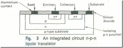
The various components making up the circuit are fabricated by means of a number of n-type and p-type regions which are diffused into the isolated regions, see Fig. 3. Once formed, the components are interconnected as required by the circuit by means of an aluminium pattern deposited on to the surface of the chip.
Integrated Circuit Bipolar Transistor
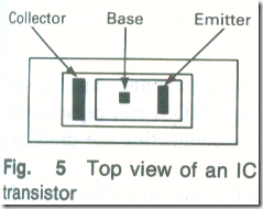
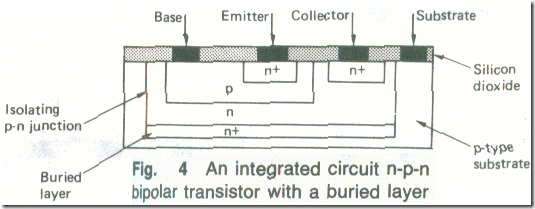
The construction of an n-p-n bipolar transistor is shown in Fig. 3 (n+ denotes a region of greater conductivity). The construction is similar to that of the silicon planar transistor, but differs from it in that the collector contact is brought out at the top of the transistor instead of at the bottom. The change in the position of the collector contact is necessary because the collector current cannot be allowed to flow in the substrate. The collector current must therefore flow in the narrow collector region and so the device has a greater collector resistance than the discrete transistor. This, undesirable, series resistance can be minimized by the use of a buried layer. The buried layer consists of an n+ low-resistance region diffused into the chip in the position shown in Fig.4. The buried layer is effectively in parallel with the collector region and it reduces the collector series resistance. The series resistance cannot be reduced by using a lower resistivity material for the collector region since this would reduce the breakdown voltage of the collector-base junction. Typically, an hfe value of about 100 is achieved. At high frequencies, the capacitance of the isolating p-n junction may possess a sufficiently low reactance to couple the collector to the substrate and adversely affect the frequency response. The top view of a bipolar transistor is shown by Fig5.
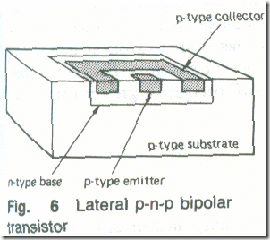
 The fabrication of a p-n-p transistor is not as simple or as cheap because additional p-type and n-type regions are required. Alternatively, a different and less efficient layout known as a lateral transistor can be employed which is more expensive and which provides a lower current gain of about 5 (see Fig. 6). Because of the difficulties associated with the use of the p-n-p transistor, its use in an integrated circuit is avoided as much as possible.
Integrated Circuit MOSFET
Most of the MOSFETs employed in digital ICs are n-channel enhancement mode devices. Depletion-mode MOSFETs are not often used and when they are they are generally connected to act as a resistor. P-channel MOSFETs are mainly used in with n-channel devices to form complementary pairs in the CMOS logic family.
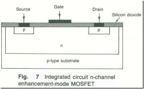
The fabrication of an n-channel integrated circuit MOSFET is shown by Fig.7. The MOSFET has an advantage over the bipolar transistor in that it is self-isolating; the drain and source regions are each isolated from the substrate by their individual p-n junctions, while the gate terminal is isolated by a layer of silicon dioxide. This feature allows a MOSFET to be formed in a smaller area of the chip than can be achieved with a bipolar transistor. Because of this MOSFETs are employed in all ICs that include a large number, perhaps many thousands, of transistors. Also, required resistance and capacitance values, if not too large, are often provided by a MOSFET, capacitance by a reverse-biased junction, resistance by connecting the drain to the gate.
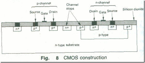 Fig. 8 . shows how a pair of MOSFETs, one an n-channel and the other a p-channel device, are formed within a CMOS 1C. The n-channel FETs are formed within a p-type isolation region. The p+ and n* regions, labelled as slops, are necessary to avoid an unwanted channel being induced between adjacent transistors. Because of the need to insert these stops a CMOS 1C occupies a greater chip area than an NMOS 1C.
Integrated Circuit JFET
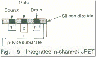
The JFET is mainly used in some linear integrated circuits for its high input impedance. Fig. 9 shows the construction of an integrated n-channel JFET.
Integrated Circuit Diode
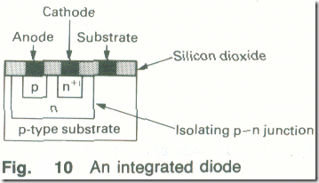
Fig. 10 shows the construction of an integrated circuit diode. The diode is formed at the same time as one of the junctions of a transistor and consists of a p-type region (the anode) and an n-type region (the cathode). An n+ region is diffused into the chip to reduce the resistance of die cathode contact.

