Integrated Circuit Capacitor
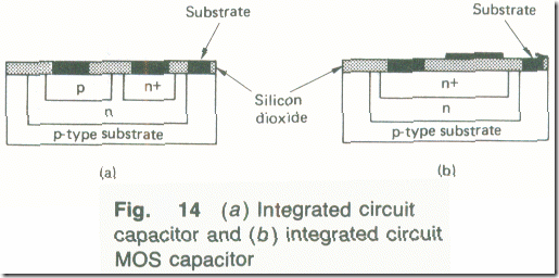
Integrated capacitors can be fabricated in two ways: either the capacitance of a reverse-biased p-n junction can be utilized, or the capacitance can be provided by a layer of silicon dioxide separating two conducting areas. The construction of a junction-type capacitor is shown in Fig. 14(a). The p-n junction is formed at the same time as either the emitter-base or the collector-base junction of a transistor. Provided the p-n junction is held in the reverse-biased condition, a capacitance of about 0.2 pF/mil can be obtained. Since the area of the chip available for a capacitor is limited, values of up to about 100 pF are available. Fig. 14(b) shows a MOS capacitor; one electrode of the capacitor is provided by an aluminium layer that is deposited on to the top of the silicon layer and the other electrode is produced by the diffused n+ region. The capacitance provided depends on the thickness of the silicon dioxide layer and the area of the aluminium plate; up to a few hundred picofarads can be achieved .
The MOS capacitor is more expensive to provide but has the following advantages over the junction capacitor: it can have voltages of either polarity applied to it, it has lower losses and a larger breakdown voltage, and its capacitance value does not depend on the magnitude of the voltage applied across the capacitor.
Large values of capacitance cannot be provided within an IC; if required the capacitance must be supplied by an external component connected to the appropriate terminals of the IC.

