Integrated Circuit Design:Introduction ,An Overview of the IC Design Process,General Considerations in IC Design,Device Scaling , Geometric Design Rules ,Design of Small-Scale and Medium-Scale Integrated Circuits ,NMOS Inverters and NMOS Gates .

Introduction

Integrated circuits (ICs) are classified according to their levels of complexity: small-scale integration (SSI), medium-scale integration (MSI), large-scale integration (LSI) and very large-scale integration (VLSI). They are also classified according to the technology employed for their fabrication (bipolar, N metal oxide semiconductor (NMOS), complementary metal oxide semiconductor (CMOS), etc.). The design of integrated circuits needs to be addressed at the SSI, MSI, LSI, and VLSI levels. Digital SSI and MSI typically consist of gates and combinations of gates. Design of digital SSI and MSI is presented in Sec. 6.3, and consists largely of the design of standard gates. These standard gates are designed to have large noise margins, large fan out, and large load current capability, in order to maximize their versatility.

In principle, the basic gates are sufficient for the design of any digital integrated circuit, no matter how complex. In practice, modifications are necessary in the basic gates and MSI circuits like flip-flops, registers, adders, etc., when such circuits are to be employed in LSI or VLSI design. For example, circuits to be interconnected on the same chip can be designed with lower noise margins, reduced load driving capability, and smaller logic swing. The resulting benefits are lower power consumption, greater circuit density, and improved reliability. On the other hand, several methodologies have emerged in LSI and VLSI design that are not based on interconnections or modification of SSI and MSI circuits. Both approaches to LSI and VLSI design are presented in the following sections.

An Overview of the IC Design Process

The effort required for the design of an integrated circuit depends on the complexity of the circuit. The requirement may range from several days effort for a single designer to several months work for a team of designers. Custom design of complex integrated circuits is the most demanding. By contrast, semicustom design of LSI and VLSI that utilize preexisting designs, such as standard cells and gate arrays, requires less design effort.

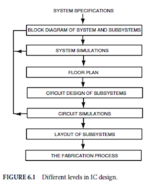
IC design is performed at many different levels and Fig. 6.1 is a nonunique depiction of these levels. Level 1 presents the design in terms of subsystems (standardcells, gate arrays, custom subcircuits, etc.) and their interconnections. Design of the sys- tem layout begins with the floor plan of level 3. It does not involve the layout of individual transistors and devices, but is concerned with the geometric arrangement and interconnection of the subsystems. Level 4 involves the circuit design of the subsystems. Levels 2 and 5 involve system and subcircuit simulations, respectively, which may lead to modifications in levels 1 and/or 4.

Discussion here will focus primarily on the sys- tem design of level 1 and the subsystem circuit de- sign of level 4. Lumped under the fabrication process of level 7 are many tasks, such as mask generation, process simulation, wafer fabrication, testing, etc. Broadly speaking, floor plan generation is a part of layout. For large ICs, layout design is often relevant to system and circuit design.

image

General Considerations in IC Design

Layout or actual arrangement of components on an IC is a design process involving design tradeoffs. Circuit design often influences layout and vice versa, especially in LSI and VLSI. Thus, it is helpful to outline some general considerations in IC design:

  • ircuit components: Chip area is crucial in IC design. The usual IC components are transistors, resistors, and capacitors. Inductors are uneconomical in area requirements and are hardly ever used in ICs except in certain microwave applications. Transistors require small chip areas and are heavily utilized in ICs. Resistor area requirements increase with resistor values. IC resistors generally range between 50 and 100 k. Capacitors are area intensive and tend to be limited to 100 pF.
  •  Isolation regions: Usually, different components would be placed in different isolation regions. The number of isolation regions, however, should be minimized in the interest of chip area economy by placing more than one component in an isolation region whenever possible. For example, several resistors could share one isolation region.
  •  Design rules: Geometric design rules that specify minimum dimensions for features and separation between features must be followed for a given IC process.
  • Power dissipation: Chip layout should allow for adequate power dissipation and avoid overheating or development of hot spots on the chip. In low-power circuits such as CMOS ICs, device size is determined by lithographic constraints. In circuits with appreciable power dissipation, device size is determined by thermal constraints and may be much larger than lithographic constraints would allow.

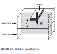
Device size determination from power-density con- siderations is illustrated with the aid of Fig. 6.2. The device resides close to the surface of the substrate. Thus, heat flow is approximately one-dimensional, from the device to the substrate, although it is actually a three-dimensional flow. Assuming an infinite heat sink of ambient temperature TA, substrate thickness ΘX, thermal conductivity α, device of surface area A, and temperature TA + ΘT , the rate of heat flow toward the heat sink, d Q/dt, is given by

image

The power density or power dissipation per unit area of the device is

image

imageDevice Scaling

The trend in IC design, especially VLSI, is progressively toward smaller sizes. Scaling techniques permit the design of circuits that can be shrunk as technological developments allow progressively smaller sizes. Two basic approaches to scaling are full scaling and constant voltage scaling.

  • Full scaling: All device dimensions, both surface and vertical, and all voltages are reduced by the same scaling factor S.
  •  Constant voltage (CV) scaling: All device dimensions, both surface and vertical, are reduced by the same scaling factor S, but voltages are not scaled. Voltages are maintained at levels compatible with
  • transistor-transistor logic (TTL) supply voltages and logic levels.

Scaling of device dimensions has implications for other device parameters. Full scaling tends to maintain constant electric field strength and, hence, parameters that are no worse off, as device dimensions are reduced, but does not ensure TTL voltage compatibility. Table 6.1 compares effect on device parameters
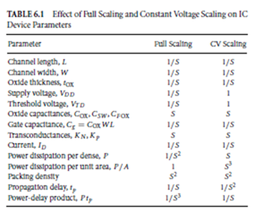
imageof the two scaling approaches. A compromise that is often adopted is to use full scaling for all internal circuits and maintain TTL voltage compatibility at the chip input/output (I/O) pins.

Although many scaling relationships are common to MOS field effect transistors (MOSFETs) and bipolar ICs (Keyes, 1975), the scaling relationships of Table 6.1 more strictly applies to MOSFETs. Bipolar doping levels, unlike MOSFETs, are not limited by oxide breakdown. Thus, in principle, miniaturization can be carried further in bipolar processing technology. However, bipolar scaling is more complex. One reason is that the junction voltages required to turn on a bipolar junction transistor (BJT) does not scale down with dimensions.

Geometric Design Rules

Design rules specify minimum device dimensions, minimum separation between features and maximum misalignment of features on an IC. Such rules tend to be process and equipment dependent. For example, a design rule for a 2-µm process may not be appropriate for a 0.5-µm process. Design rules should protect against fatal errors such as short circuits due to excessive misalignment of features, or open circuits due to too narrow a metal or polysilicon conductive path.

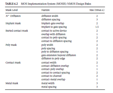
Generalized design rules that are portable between processes and scalable to facilitate adaptation to shrinking minimum geometries as processes evolve are desirable. Other advantages of generalized design rules include increased design efficiency due to fewer levels and fewer rules, automatic translation to final layout, layout-rule and electrical-rule checking, simulation, verification, etc. The Mead-Conway approach (1980) to generalized design rules is to define a scalable and process-dependent parameter, lambda (λ), as the maximum misalignment of a feature from its intended position on a wafer or half the maximum misalignment of two features on different mask layers. Table 6.2 shows a version of the Mead-Conway scalable design rules for NMOS (Fabricius, 1990).

CMOS ICs utilize both NMOS and PMOS devices. Starting with a p-substrate, the NMOS would be fabricated on the p-substrate and the PMOS in an n-well, and vice versa. With the addition of an n-well, p-well or twin tub process, CMOS fabrication is similar to that for NMOS, although more complex. Table 6.3 (Fabricius, 1990) shows the Mead-Conway scalable CMOS design rules. The dimensions are given in multiples of λ and the rules are specified by the MOS Implementation System (MOSIS) of the

image

image

image

University of Southern California Information Sciences Institute. Further clarification of the rules may be obtained from MOSIS manuals (USCISI, 1984, 1988).

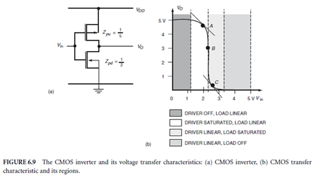
Figure 6.3 illustrates the layout of an NMOS inverter with depletion load and a CMOS inverter, employing the NMOS and CMOS scalable design rules just discussed. Figure 6.3(a) and Figure 6.3(b) show the circuit diagrams for the NMOS and CMOS, respectively, with the aspect ratios Z defined as the ratio of the length to the width of a transistor gate. Figure 6.3(c) and Figure 6.3(d) give the layouts for the NMOS and CMOS, respectively.

A simplified design rule for a bipolar npn comparable to those previously discussed for NMOS and CMOS is presented in Table 6.4. As before, the minimum size of a feature in the layout is denoted by lambda (λ). The following six masks are required for the fabrication: n+ buried-layer diffusion, p+ isolation diffusion, p base region diffusion, n+ emitter and collector diffusions, contact windows, and metalization.

Design of Small-Scale and Medium-Scale Integrated Circuits

Gates are the basic building blocks in digital integrated circuits. Small-scale integrated circuits are essentially gate circuits, and medium-scale integrated circuits are circuits employing several gates. Gates, in turn, are based on inverters and can be realized from inverter circuits with some modifications, especially those modifications that allow for multiple inputs. This section will start with a discussion of inverters and gates.

image

NMOS Inverters

A resistive load NMOS inverter, its output characteristics, and its voltage transfer characteristic are shown in Fig. 6.4. The loadline is also shown on the output characteristics. Resistive load inverters are not widely used in ICs because resistors require long strips and, hence, large areas on the chip. A solution to this problem is to use active loads, since transistors are economical in chip area.
image

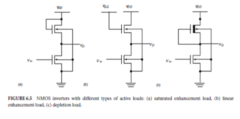
imageFigure 6.5 shows three NMOS inverters with three types of NMOS active loads: saturated enhancement load, linear enhancement load, and depletion load. One basis for comparison between these inverters is the geometric ratio K R , which is defined as Zpu/Zpd. Z denotes the ratio of length to width of a transistor channel. The subscript pu refers to the pull-up or load device, whereas the subscript pd refers to the pull-down or driving transistor.

The saturated enhancement load inverter overcomes much of the area disadvantage of the resistive load inverter. When carrying the same current and having the same pull-down transistor as the resistive inverter, however, K R is large for the saturated enhancement load inverter, indicating load transistor area minimization is still possible. This configuration yields a smaller logic swing relative to the resistive load inverter, however, because the load transistor stops conducting when its VGS = VDS decreases to VT . Thus, for this inverter, VOH = VDD VT .

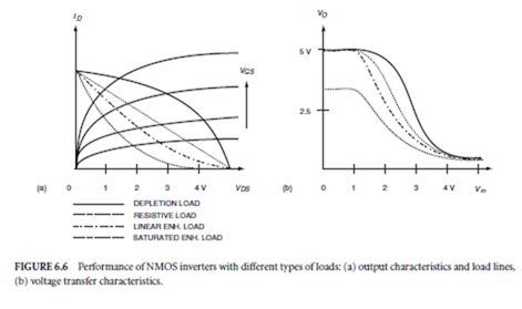
In Fig. 6.5(b), because VGG is greater than VD D + VT , VDS is always smaller than VG S VT ; thus, the load always operates in the linear region. This results in a linear enhancement load NMOS inverter. The high value of VGG also ensures that VGS is always greater than VT , so that the load remains on and VOH pulls up to VDD . The linear enhancement load configuration, however, requires a load transistor of larger area relative to the saturated enhancement load inverter, and requires additional chip area for the VGG contact. In the depletion NMOS load inverter of Fig. 6.5(c), VGS = 0, thus the load device is always on and VOH pulls all the way to VDD . This configuration overcomes the area disadvantage without incurring a voltage swing penalty. It is, therefore, the preferred alternative. The performance of the NMOS inverters with the four different types of loads are graphically compared in Fig. 6.6(a) and Fig. 6.6(b). Both the loadlines and the voltage transfer characteristics were obtained from SPICE simulation. Figure 6.6(a) shows the loadlines superimposed on the output characteristics of the pull-down transistor, which is the same for the four inverters. RL is 100 kand each inverter has VDD = 5 V, VOL = 0.2 V and ID max = 48 µA. Note that VOH falls short of VDD for the saturated enhancement load inverter but not for the others. Figure 6.6(b) shows the voltage transfer characteristics (VTC) for the four inverters. VOH is again shown to be less than VDD for the saturated enhancement load. Note, also, that the depletion load VTC more closely approaches the ideal inverter VTC than any of the others.

The loadlines of Fig. 6.5(a) are easy to generate. Consider, for example the depletion NMOS load. VGS is fixed at 0 V, so that its output characteristic consists of only the curve for VGS = 0. ID is always the same for the load and driving transistor, but their VDS add up to VDD . Thus, when VDS is high for one transistor, it is low for the other. The loadline is obtained by shifting the origin for VDS for the load characteristic to VDD , reflecting it about the vertical axis through VDD and superimposing it on the V I characteristics for the driving inverter.

image

The voltage transfer characteristics are best generated by computer simulation. Useful insights, however, can be gained from an analysis yielding the critical voltages VO H , VO L , VI H , VIL , and VO for any specified Vin. The NMOS currents hold the key to such an analysis. Threshold voltages are different for enhancement and depletion NMOS transistors, but the drain current equations are the same. The drain current is given in the linear region and the saturated region, respectively, by

imageSimilar definitions apply to PMOS transistors.

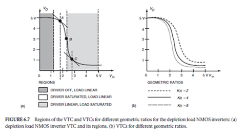
Consider the VTC of Fig. 6.7(a) for a depletion load NMOS inverter. For the region 0 < Vin < VT the driving transistor is off, so VOH = VDD . At A, Vin is small; thus, for the driving transistor, VDS = VO > Vin − VT = VGS VT . For the load VDS = VDD VO is small. Hence, the driver is saturated and load is linear. Similar considerations lead to the conclusions as to the region in which each device operates, as noted in the figure. To find VIL and VIH , the drain currents for the appropriate region of operation for points A and C, respectively, are equated, for both transistors. Differentiating the resulting equations with respect to Vin and applying the condition that d VO /d Vin = −1 yields the required critical voltages. Equating drain currents for saturated load and linear driver at Vin = VDD and solving yields VOL . The output voltage VO may be found at any value of Vin by equating the drain currents for the two transistors, appropriate for that region of Vin, and solving for VO at the given Vin.

NMOS Gates

Only NOR and NAND need be considered because these are more economical in chip area than OR and AND, and any logic system can be implemented entirely with either NOR or NAND. By connecting driving
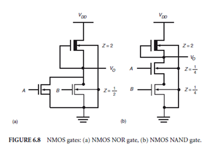
imagetransistors in parallel to provide the multiple inputs, the NMOS inverter is easily converted to a NOR gate as shown in Fig. 6.8(a). By connecting driving transistors in series as in Fig. 6.8(b), an NAND gate is obtained.

The NMOS, NOR, and NAND gates are essentially modifications of the depletion load NMOS inverter of Fig. 6.5(c). They all have the same depletion load, and their performance should be similar. For the same value of VDD , each has VOH = VDD , and they should have the same VOL and the same drain current when VO = VO L . In Fig. 6.5(c), the depletion load inverter has Zpu = 2, Zpd = 1/2 and K R = 4. Thus, Zpu is 2 for the NOR and the NAND gate. With only one driving transistor on in the NOR gate, the drain current should be sufficient to ensure that VO = VO L . Thus, for each of the driving transistors, ZI = 1/2 , as for the depletion load inverter. For the NAND gate, the equivalent series combination of Zpd (proportional to drain-source resistance) should also be 1 to allow the same value of VO , leading to ZI = 1 for each driving transistor in the NAND gate. Thus, K R is 4 for the inverter, 4 for the NOR gate, and 8 for the NAND. As the number of inputs increases, K R increases for the NAND but not for the NOR. It is clear that NMOS

image

image

NAND gates are wasteful of chip area relative to NMOS NOR. Hence, NOR gates are preferred (and the NOR is the standard gate) in NMOS.

Leave a comment

Your email address will not be published. Required fields are marked *

Integrated Circuit Design:Introduction ,An Overview of the IC Design Process,General Considerations in IC Design,Device Scaling , Geometric Design Rules ,Design of Small-Scale and Medium-Scale Integrated Circuits ,NMOS Inverters and NMOS Gates .

Introduction

Integrated circuits (ICs) are classified according to their levels of complexity: small-scale integration (SSI), medium-scale integration (MSI), large-scale integration (LSI) and very large-scale integration (VLSI). They are also classified according to the technology employed for their fabrication (bipolar, N metal oxide semiconductor (NMOS), complementary metal oxide semiconductor (CMOS), etc.). The design of integrated circuits needs to be addressed at the SSI, MSI, LSI, and VLSI levels. Digital SSI and MSI typically consist of gates and combinations of gates. Design of digital SSI and MSI is presented in Sec. 6.3, and consists largely of the design of standard gates. These standard gates are designed to have large noise margins, large fan out, and large load current capability, in order to maximize their versatility.

In principle, the basic gates are sufficient for the design of any digital integrated circuit, no matter how complex. In practice, modifications are necessary in the basic gates and MSI circuits like flip-flops, registers, adders, etc., when such circuits are to be employed in LSI or VLSI design. For example, circuits to be interconnected on the same chip can be designed with lower noise margins, reduced load driving capability, and smaller logic swing. The resulting benefits are lower power consumption, greater circuit density, and improved reliability. On the other hand, several methodologies have emerged in LSI and VLSI design that are not based on interconnections or modification of SSI and MSI circuits. Both approaches to LSI and VLSI design are presented in the following sections.

An Overview of the IC Design Process

The effort required for the design of an integrated circuit depends on the complexity of the circuit. The requirement may range from several days effort for a single designer to several months work for a team of designers. Custom design of complex integrated circuits is the most demanding. By contrast, semicustom design of LSI and VLSI that utilize preexisting designs, such as standard cells and gate arrays, requires less design effort.

IC design is performed at many different levels and Fig. 6.1 is a nonunique depiction of these levels. Level 1 presents the design in terms of subsystems (standardcells, gate arrays, custom subcircuits, etc.) and their interconnections. Design of the sys- tem layout begins with the floor plan of level 3. It does not involve the layout of individual transistors and devices, but is concerned with the geometric arrangement and interconnection of the subsystems. Level 4 involves the circuit design of the subsystems. Levels 2 and 5 involve system and subcircuit simulations, respectively, which may lead to modifications in levels 1 and/or 4.

Discussion here will focus primarily on the sys- tem design of level 1 and the subsystem circuit de- sign of level 4. Lumped under the fabrication process of level 7 are many tasks, such as mask generation, process simulation, wafer fabrication, testing, etc. Broadly speaking, floor plan generation is a part of layout. For large ICs, layout design is often relevant to system and circuit design.

image

General Considerations in IC Design

Layout or actual arrangement of components on an IC is a design process involving design tradeoffs. Circuit design often influences layout and vice versa, especially in LSI and VLSI. Thus, it is helpful to outline some general considerations in IC design:

  • ircuit components: Chip area is crucial in IC design. The usual IC components are transistors, resistors, and capacitors. Inductors are uneconomical in area requirements and are hardly ever used in ICs except in certain microwave applications. Transistors require small chip areas and are heavily utilized in ICs. Resistor area requirements increase with resistor values. IC resistors generally range between 50 and 100 k. Capacitors are area intensive and tend to be limited to 100 pF.
  •  Isolation regions: Usually, different components would be placed in different isolation regions. The number of isolation regions, however, should be minimized in the interest of chip area economy by placing more than one component in an isolation region whenever possible. For example, several resistors could share one isolation region.
  •  Design rules: Geometric design rules that specify minimum dimensions for features and separation between features must be followed for a given IC process.
  • Power dissipation: Chip layout should allow for adequate power dissipation and avoid overheating or development of hot spots on the chip. In low-power circuits such as CMOS ICs, device size is determined by lithographic constraints. In circuits with appreciable power dissipation, device size is determined by thermal constraints and may be much larger than lithographic constraints would allow.

Device size determination from power-density con- siderations is illustrated with the aid of Fig. 6.2. The device resides close to the surface of the substrate. Thus, heat flow is approximately one-dimensional, from the device to the substrate, although it is actually a three-dimensional flow. Assuming an infinite heat sink of ambient temperature TA, substrate thickness ΘX, thermal conductivity α, device of surface area A, and temperature TA + ΘT , the rate of heat flow toward the heat sink, d Q/dt, is given by

image

The power density or power dissipation per unit area of the device is

image

imageDevice Scaling

The trend in IC design, especially VLSI, is progressively toward smaller sizes. Scaling techniques permit the design of circuits that can be shrunk as technological developments allow progressively smaller sizes. Two basic approaches to scaling are full scaling and constant voltage scaling.

  • Full scaling: All device dimensions, both surface and vertical, and all voltages are reduced by the same scaling factor S.
  •  Constant voltage (CV) scaling: All device dimensions, both surface and vertical, are reduced by the same scaling factor S, but voltages are not scaled. Voltages are maintained at levels compatible with
  • transistor-transistor logic (TTL) supply voltages and logic levels.

Scaling of device dimensions has implications for other device parameters. Full scaling tends to maintain constant electric field strength and, hence, parameters that are no worse off, as device dimensions are reduced, but does not ensure TTL voltage compatibility. Table 6.1 compares effect on device parameters

imageof the two scaling approaches. A compromise that is often adopted is to use full scaling for all internal circuits and maintain TTL voltage compatibility at the chip input/output (I/O) pins.

Although many scaling relationships are common to MOS field effect transistors (MOSFETs) and bipolar ICs (Keyes, 1975), the scaling relationships of Table 6.1 more strictly applies to MOSFETs. Bipolar doping levels, unlike MOSFETs, are not limited by oxide breakdown. Thus, in principle, miniaturization can be carried further in bipolar processing technology. However, bipolar scaling is more complex. One reason is that the junction voltages required to turn on a bipolar junction transistor (BJT) does not scale down with dimensions.

Geometric Design Rules

Design rules specify minimum device dimensions, minimum separation between features and maximum misalignment of features on an IC. Such rules tend to be process and equipment dependent. For example, a design rule for a 2-µm process may not be appropriate for a 0.5-µm process. Design rules should protect against fatal errors such as short circuits due to excessive misalignment of features, or open circuits due to too narrow a metal or polysilicon conductive path.

Generalized design rules that are portable between processes and scalable to facilitate adaptation to shrinking minimum geometries as processes evolve are desirable. Other advantages of generalized design rules include increased design efficiency due to fewer levels and fewer rules, automatic translation to final layout, layout-rule and electrical-rule checking, simulation, verification, etc. The Mead-Conway approach (1980) to generalized design rules is to define a scalable and process-dependent parameter, lambda (λ), as the maximum misalignment of a feature from its intended position on a wafer or half the maximum misalignment of two features on different mask layers. Table 6.2 shows a version of the Mead-Conway scalable design rules for NMOS (Fabricius, 1990).

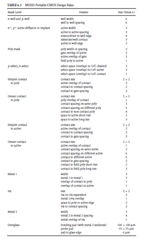
CMOS ICs utilize both NMOS and PMOS devices. Starting with a p-substrate, the NMOS would be fabricated on the p-substrate and the PMOS in an n-well, and vice versa. With the addition of an n-well, p-well or twin tub process, CMOS fabrication is similar to that for NMOS, although more complex. Table 6.3 (Fabricius, 1990) shows the Mead-Conway scalable CMOS design rules. The dimensions are given in multiples of λ and the rules are specified by the MOS Implementation System (MOSIS) of the

image

image

image

University of Southern California Information Sciences Institute. Further clarification of the rules may be obtained from MOSIS manuals (USCISI, 1984, 1988).

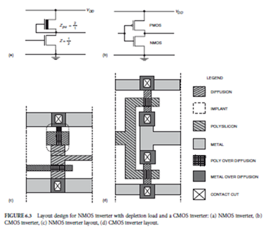
Figure 6.3 illustrates the layout of an NMOS inverter with depletion load and a CMOS inverter, employing the NMOS and CMOS scalable design rules just discussed. Figure 6.3(a) and Figure 6.3(b) show the circuit diagrams for the NMOS and CMOS, respectively, with the aspect ratios Z defined as the ratio of the length to the width of a transistor gate. Figure 6.3(c) and Figure 6.3(d) give the layouts for the NMOS and CMOS, respectively.

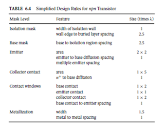
A simplified design rule for a bipolar npn comparable to those previously discussed for NMOS and CMOS is presented in Table 6.4. As before, the minimum size of a feature in the layout is denoted by lambda (λ). The following six masks are required for the fabrication: n+ buried-layer diffusion, p+ isolation diffusion, p base region diffusion, n+ emitter and collector diffusions, contact windows, and metalization.

Design of Small-Scale and Medium-Scale Integrated Circuits

Gates are the basic building blocks in digital integrated circuits. Small-scale integrated circuits are essentially gate circuits, and medium-scale integrated circuits are circuits employing several gates. Gates, in turn, are based on inverters and can be realized from inverter circuits with some modifications, especially those modifications that allow for multiple inputs. This section will start with a discussion of inverters and gates.

image

NMOS Inverters

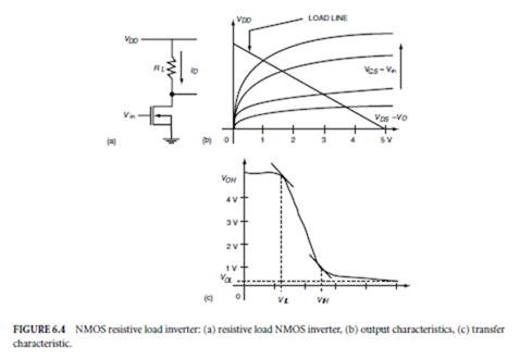
A resistive load NMOS inverter, its output characteristics, and its voltage transfer characteristic are shown in Fig. 6.4. The loadline is also shown on the output characteristics. Resistive load inverters are not widely used in ICs because resistors require long strips and, hence, large areas on the chip. A solution to this problem is to use active loads, since transistors are economical in chip area.

image

imageFigure 6.5 shows three NMOS inverters with three types of NMOS active loads: saturated enhancement load, linear enhancement load, and depletion load. One basis for comparison between these inverters is the geometric ratio K R , which is defined as Zpu/Zpd. Z denotes the ratio of length to width of a transistor channel. The subscript pu refers to the pull-up or load device, whereas the subscript pd refers to the pull-down or driving transistor.

The saturated enhancement load inverter overcomes much of the area disadvantage of the resistive load inverter. When carrying the same current and having the same pull-down transistor as the resistive inverter, however, K R is large for the saturated enhancement load inverter, indicating load transistor area minimization is still possible. This configuration yields a smaller logic swing relative to the resistive load inverter, however, because the load transistor stops conducting when its VGS = VDS decreases to VT . Thus, for this inverter, VOH = VDD VT .

In Fig. 6.5(b), because VGG is greater than VD D + VT , VDS is always smaller than VG S VT ; thus, the load always operates in the linear region. This results in a linear enhancement load NMOS inverter. The high value of VGG also ensures that VGS is always greater than VT , so that the load remains on and VOH pulls up to VDD . The linear enhancement load configuration, however, requires a load transistor of larger area relative to the saturated enhancement load inverter, and requires additional chip area for the VGG contact. In the depletion NMOS load inverter of Fig. 6.5(c), VGS = 0, thus the load device is always on and VOH pulls all the way to VDD . This configuration overcomes the area disadvantage without incurring a voltage swing penalty. It is, therefore, the preferred alternative. The performance of the NMOS inverters with the four different types of loads are graphically compared in Fig. 6.6(a) and Fig. 6.6(b). Both the loadlines and the voltage transfer characteristics were obtained from SPICE simulation. Figure 6.6(a) shows the loadlines superimposed on the output characteristics of the pull-down transistor, which is the same for the four inverters. RL is 100 kand each inverter has VDD = 5 V, VOL = 0.2 V and ID max = 48 µA. Note that VOH falls short of VDD for the saturated enhancement load inverter but not for the others. Figure 6.6(b) shows the voltage transfer characteristics (VTC) for the four inverters. VOH is again shown to be less than VDD for the saturated enhancement load. Note, also, that the depletion load VTC more closely approaches the ideal inverter VTC than any of the others.

The loadlines of Fig. 6.5(a) are easy to generate. Consider, for example the depletion NMOS load. VGS is fixed at 0 V, so that its output characteristic consists of only the curve for VGS = 0. ID is always the same for the load and driving transistor, but their VDS add up to VDD . Thus, when VDS is high for one transistor, it is low for the other. The loadline is obtained by shifting the origin for VDS for the load characteristic to VDD , reflecting it about the vertical axis through VDD and superimposing it on the V I characteristics for the driving inverter.

image

The voltage transfer characteristics are best generated by computer simulation. Useful insights, however, can be gained from an analysis yielding the critical voltages VO H , VO L , VI H , VIL , and VO for any specified Vin. The NMOS currents hold the key to such an analysis. Threshold voltages are different for enhancement and depletion NMOS transistors, but the drain current equations are the same. The drain current is given in the linear region and the saturated region, respectively, by

imageSimilar definitions apply to PMOS transistors.

Consider the VTC of Fig. 6.7(a) for a depletion load NMOS inverter. For the region 0 < Vin < VT the driving transistor is off, so VOH = VDD . At A, Vin is small; thus, for the driving transistor, VDS = VO > Vin − VT = VGS VT . For the load VDS = VDD VO is small. Hence, the driver is saturated and load is linear. Similar considerations lead to the conclusions as to the region in which each device operates, as noted in the figure. To find VIL and VIH , the drain currents for the appropriate region of operation for points A and C, respectively, are equated, for both transistors. Differentiating the resulting equations with respect to Vin and applying the condition that d VO /d Vin = −1 yields the required critical voltages. Equating drain currents for saturated load and linear driver at Vin = VDD and solving yields VOL . The output voltage VO may be found at any value of Vin by equating the drain currents for the two transistors, appropriate for that region of Vin, and solving for VO at the given Vin.

NMOS Gates

Only NOR and NAND need be considered because these are more economical in chip area than OR and AND, and any logic system can be implemented entirely with either NOR or NAND. By connecting driving

imagetransistors in parallel to provide the multiple inputs, the NMOS inverter is easily converted to a NOR gate as shown in Fig. 6.8(a). By connecting driving transistors in series as in Fig. 6.8(b), an NAND gate is obtained.

The NMOS, NOR, and NAND gates are essentially modifications of the depletion load NMOS inverter of Fig. 6.5(c). They all have the same depletion load, and their performance should be similar. For the same value of VDD , each has VOH = VDD , and they should have the same VOL and the same drain current when VO = VO L . In Fig. 6.5(c), the depletion load inverter has Zpu = 2, Zpd = 1/2 and K R = 4. Thus, Zpu is 2 for the NOR and the NAND gate. With only one driving transistor on in the NOR gate, the drain current should be sufficient to ensure that VO = VO L . Thus, for each of the driving transistors, ZI = 1/2 , as for the depletion load inverter. For the NAND gate, the equivalent series combination of Zpd (proportional to drain-source resistance) should also be 1 to allow the same value of VO , leading to ZI = 1 for each driving transistor in the NAND gate. Thus, K R is 4 for the inverter, 4 for the NOR gate, and 8 for the NAND. As the number of inputs increases, K R increases for the NAND but not for the NOR. It is clear that NMOS

image

image

NAND gates are wasteful of chip area relative to NMOS NOR. Hence, NOR gates are preferred (and the NOR is the standard gate) in NMOS.
Leave a comment

Your email address will not be published. Required fields are marked *

Integrated Circuit Design:Introduction ,An Overview of the IC Design Process,General Considerations in IC Design,Device Scaling , Geometric Design Rules ,Design of Small-Scale and Medium-Scale Integrated Circuits ,NMOS Inverters and NMOS Gates .

Introduction

Integrated circuits (ICs) are classified according to their levels of complexity: small-scale integration (SSI), medium-scale integration (MSI), large-scale integration (LSI) and very large-scale integration (VLSI). They are also classified according to the technology employed for their fabrication (bipolar, N metal oxide semiconductor (NMOS), complementary metal oxide semiconductor (CMOS), etc.). The design of integrated circuits needs to be addressed at the SSI, MSI, LSI, and VLSI levels. Digital SSI and MSI typically consist of gates and combinations of gates. Design of digital SSI and MSI is presented in Sec. 6.3, and consists largely of the design of standard gates. These standard gates are designed to have large noise margins, large fan out, and large load current capability, in order to maximize their versatility.

In principle, the basic gates are sufficient for the design of any digital integrated circuit, no matter how complex. In practice, modifications are necessary in the basic gates and MSI circuits like flip-flops, registers, adders, etc., when such circuits are to be employed in LSI or VLSI design. For example, circuits to be interconnected on the same chip can be designed with lower noise margins, reduced load driving capability, and smaller logic swing. The resulting benefits are lower power consumption, greater circuit density, and improved reliability. On the other hand, several methodologies have emerged in LSI and VLSI design that are not based on interconnections or modification of SSI and MSI circuits. Both approaches to LSI and VLSI design are presented in the following sections.

An Overview of the IC Design Process

The effort required for the design of an integrated circuit depends on the complexity of the circuit. The requirement may range from several days effort for a single designer to several months work for a team of designers. Custom design of complex integrated circuits is the most demanding. By contrast, semicustom design of LSI and VLSI that utilize preexisting designs, such as standard cells and gate arrays, requires less design effort.

IC design is performed at many different levels and Fig. 6.1 is a nonunique depiction of these levels. Level 1 presents the design in terms of subsystems (standardcells, gate arrays, custom subcircuits, etc.) and their interconnections. Design of the sys- tem layout begins with the floor plan of level 3. It does not involve the layout of individual transistors and devices, but is concerned with the geometric arrangement and interconnection of the subsystems. Level 4 involves the circuit design of the subsystems. Levels 2 and 5 involve system and subcircuit simulations, respectively, which may lead to modifications in levels 1 and/or 4.

Discussion here will focus primarily on the sys- tem design of level 1 and the subsystem circuit de- sign of level 4. Lumped under the fabrication process of level 7 are many tasks, such as mask generation, process simulation, wafer fabrication, testing, etc. Broadly speaking, floor plan generation is a part of layout. For large ICs, layout design is often relevant to system and circuit design.

image

General Considerations in IC Design

Layout or actual arrangement of components on an IC is a design process involving design tradeoffs. Circuit design often influences layout and vice versa, especially in LSI and VLSI. Thus, it is helpful to outline some general considerations in IC design:

  • ircuit components: Chip area is crucial in IC design. The usual IC components are transistors, resistors, and capacitors. Inductors are uneconomical in area requirements and are hardly ever used in ICs except in certain microwave applications. Transistors require small chip areas and are heavily utilized in ICs. Resistor area requirements increase with resistor values. IC resistors generally range between 50 and 100 k. Capacitors are area intensive and tend to be limited to 100 pF.
  •  Isolation regions: Usually, different components would be placed in different isolation regions. The number of isolation regions, however, should be minimized in the interest of chip area economy by placing more than one component in an isolation region whenever possible. For example, several resistors could share one isolation region.
  •  Design rules: Geometric design rules that specify minimum dimensions for features and separation between features must be followed for a given IC process.
  • Power dissipation: Chip layout should allow for adequate power dissipation and avoid overheating or development of hot spots on the chip. In low-power circuits such as CMOS ICs, device size is determined by lithographic constraints. In circuits with appreciable power dissipation, device size is determined by thermal constraints and may be much larger than lithographic constraints would allow.

Device size determination from power-density con- siderations is illustrated with the aid of Fig. 6.2. The device resides close to the surface of the substrate. Thus, heat flow is approximately one-dimensional, from the device to the substrate, although it is actually a three-dimensional flow. Assuming an infinite heat sink of ambient temperature TA, substrate thickness ΘX, thermal conductivity α, device of surface area A, and temperature TA + ΘT , the rate of heat flow toward the heat sink, d Q/dt, is given by

image

The power density or power dissipation per unit area of the device is

image

imageDevice Scaling

The trend in IC design, especially VLSI, is progressively toward smaller sizes. Scaling techniques permit the design of circuits that can be shrunk as technological developments allow progressively smaller sizes. Two basic approaches to scaling are full scaling and constant voltage scaling.

  • Full scaling: All device dimensions, both surface and vertical, and all voltages are reduced by the same scaling factor S.
  •  Constant voltage (CV) scaling: All device dimensions, both surface and vertical, are reduced by the same scaling factor S, but voltages are not scaled. Voltages are maintained at levels compatible with
  • transistor-transistor logic (TTL) supply voltages and logic levels.

Scaling of device dimensions has implications for other device parameters. Full scaling tends to maintain constant electric field strength and, hence, parameters that are no worse off, as device dimensions are reduced, but does not ensure TTL voltage compatibility. Table 6.1 compares effect on device parameters

imageof the two scaling approaches. A compromise that is often adopted is to use full scaling for all internal circuits and maintain TTL voltage compatibility at the chip input/output (I/O) pins.

Although many scaling relationships are common to MOS field effect transistors (MOSFETs) and bipolar ICs (Keyes, 1975), the scaling relationships of Table 6.1 more strictly applies to MOSFETs. Bipolar doping levels, unlike MOSFETs, are not limited by oxide breakdown. Thus, in principle, miniaturization can be carried further in bipolar processing technology. However, bipolar scaling is more complex. One reason is that the junction voltages required to turn on a bipolar junction transistor (BJT) does not scale down with dimensions.

Geometric Design Rules

Design rules specify minimum device dimensions, minimum separation between features and maximum misalignment of features on an IC. Such rules tend to be process and equipment dependent. For example, a design rule for a 2-µm process may not be appropriate for a 0.5-µm process. Design rules should protect against fatal errors such as short circuits due to excessive misalignment of features, or open circuits due to too narrow a metal or polysilicon conductive path.

Generalized design rules that are portable between processes and scalable to facilitate adaptation to shrinking minimum geometries as processes evolve are desirable. Other advantages of generalized design rules include increased design efficiency due to fewer levels and fewer rules, automatic translation to final layout, layout-rule and electrical-rule checking, simulation, verification, etc. The Mead-Conway approach (1980) to generalized design rules is to define a scalable and process-dependent parameter, lambda (λ), as the maximum misalignment of a feature from its intended position on a wafer or half the maximum misalignment of two features on different mask layers. Table 6.2 shows a version of the Mead-Conway scalable design rules for NMOS (Fabricius, 1990).

CMOS ICs utilize both NMOS and PMOS devices. Starting with a p-substrate, the NMOS would be fabricated on the p-substrate and the PMOS in an n-well, and vice versa. With the addition of an n-well, p-well or twin tub process, CMOS fabrication is similar to that for NMOS, although more complex. Table 6.3 (Fabricius, 1990) shows the Mead-Conway scalable CMOS design rules. The dimensions are given in multiples of λ and the rules are specified by the MOS Implementation System (MOSIS) of the

image

image

image

University of Southern California Information Sciences Institute. Further clarification of the rules may be obtained from MOSIS manuals (USCISI, 1984, 1988).

Figure 6.3 illustrates the layout of an NMOS inverter with depletion load and a CMOS inverter, employing the NMOS and CMOS scalable design rules just discussed. Figure 6.3(a) and Figure 6.3(b) show the circuit diagrams for the NMOS and CMOS, respectively, with the aspect ratios Z defined as the ratio of the length to the width of a transistor gate. Figure 6.3(c) and Figure 6.3(d) give the layouts for the NMOS and CMOS, respectively.

A simplified design rule for a bipolar npn comparable to those previously discussed for NMOS and CMOS is presented in Table 6.4. As before, the minimum size of a feature in the layout is denoted by lambda (λ). The following six masks are required for the fabrication: n+ buried-layer diffusion, p+ isolation diffusion, p base region diffusion, n+ emitter and collector diffusions, contact windows, and metalization.

Design of Small-Scale and Medium-Scale Integrated Circuits

Gates are the basic building blocks in digital integrated circuits. Small-scale integrated circuits are essentially gate circuits, and medium-scale integrated circuits are circuits employing several gates. Gates, in turn, are based on inverters and can be realized from inverter circuits with some modifications, especially those modifications that allow for multiple inputs. This section will start with a discussion of inverters and gates.

image

NMOS Inverters

A resistive load NMOS inverter, its output characteristics, and its voltage transfer characteristic are shown in Fig. 6.4. The loadline is also shown on the output characteristics. Resistive load inverters are not widely used in ICs because resistors require long strips and, hence, large areas on the chip. A solution to this problem is to use active loads, since transistors are economical in chip area.

image

imageFigure 6.5 shows three NMOS inverters with three types of NMOS active loads: saturated enhancement load, linear enhancement load, and depletion load. One basis for comparison between these inverters is the geometric ratio K R , which is defined as Zpu/Zpd. Z denotes the ratio of length to width of a transistor channel. The subscript pu refers to the pull-up or load device, whereas the subscript pd refers to the pull-down or driving transistor.

The saturated enhancement load inverter overcomes much of the area disadvantage of the resistive load inverter. When carrying the same current and having the same pull-down transistor as the resistive inverter, however, K R is large for the saturated enhancement load inverter, indicating load transistor area minimization is still possible. This configuration yields a smaller logic swing relative to the resistive load inverter, however, because the load transistor stops conducting when its VGS = VDS decreases to VT . Thus, for this inverter, VOH = VDD VT .

In Fig. 6.5(b), because VGG is greater than VD D + VT , VDS is always smaller than VG S VT ; thus, the load always operates in the linear region. This results in a linear enhancement load NMOS inverter. The high value of VGG also ensures that VGS is always greater than VT , so that the load remains on and VOH pulls up to VDD . The linear enhancement load configuration, however, requires a load transistor of larger area relative to the saturated enhancement load inverter, and requires additional chip area for the VGG contact. In the depletion NMOS load inverter of Fig. 6.5(c), VGS = 0, thus the load device is always on and VOH pulls all the way to VDD . This configuration overcomes the area disadvantage without incurring a voltage swing penalty. It is, therefore, the preferred alternative. The performance of the NMOS inverters with the four different types of loads are graphically compared in Fig. 6.6(a) and Fig. 6.6(b). Both the loadlines and the voltage transfer characteristics were obtained from SPICE simulation. Figure 6.6(a) shows the loadlines superimposed on the output characteristics of the pull-down transistor, which is the same for the four inverters. RL is 100 kand each inverter has VDD = 5 V, VOL = 0.2 V and ID max = 48 µA. Note that VOH falls short of VDD for the saturated enhancement load inverter but not for the others. Figure 6.6(b) shows the voltage transfer characteristics (VTC) for the four inverters. VOH is again shown to be less than VDD for the saturated enhancement load. Note, also, that the depletion load VTC more closely approaches the ideal inverter VTC than any of the others.

The loadlines of Fig. 6.5(a) are easy to generate. Consider, for example the depletion NMOS load. VGS is fixed at 0 V, so that its output characteristic consists of only the curve for VGS = 0. ID is always the same for the load and driving transistor, but their VDS add up to VDD . Thus, when VDS is high for one transistor, it is low for the other. The loadline is obtained by shifting the origin for VDS for the load characteristic to VDD , reflecting it about the vertical axis through VDD and superimposing it on the V I characteristics for the driving inverter.

image

The voltage transfer characteristics are best generated by computer simulation. Useful insights, however, can be gained from an analysis yielding the critical voltages VO H , VO L , VI H , VIL , and VO for any specified Vin. The NMOS currents hold the key to such an analysis. Threshold voltages are different for enhancement and depletion NMOS transistors, but the drain current equations are the same. The drain current is given in the linear region and the saturated region, respectively, by

imageSimilar definitions apply to PMOS transistors.

Consider the VTC of Fig. 6.7(a) for a depletion load NMOS inverter. For the region 0 < Vin < VT the driving transistor is off, so VOH = VDD . At A, Vin is small; thus, for the driving transistor, VDS = VO > Vin − VT = VGS VT . For the load VDS = VDD VO is small. Hence, the driver is saturated and load is linear. Similar considerations lead to the conclusions as to the region in which each device operates, as noted in the figure. To find VIL and VIH , the drain currents for the appropriate region of operation for points A and C, respectively, are equated, for both transistors. Differentiating the resulting equations with respect to Vin and applying the condition that d VO /d Vin = −1 yields the required critical voltages. Equating drain currents for saturated load and linear driver at Vin = VDD and solving yields VOL . The output voltage VO may be found at any value of Vin by equating the drain currents for the two transistors, appropriate for that region of Vin, and solving for VO at the given Vin.

NMOS Gates

Only NOR and NAND need be considered because these are more economical in chip area than OR and AND, and any logic system can be implemented entirely with either NOR or NAND. By connecting driving

imagetransistors in parallel to provide the multiple inputs, the NMOS inverter is easily converted to a NOR gate as shown in Fig. 6.8(a). By connecting driving transistors in series as in Fig. 6.8(b), an NAND gate is obtained.

The NMOS, NOR, and NAND gates are essentially modifications of the depletion load NMOS inverter of Fig. 6.5(c). They all have the same depletion load, and their performance should be similar. For the same value of VDD , each has VOH = VDD , and they should have the same VOL and the same drain current when VO = VO L . In Fig. 6.5(c), the depletion load inverter has Zpu = 2, Zpd = 1/2 and K R = 4. Thus, Zpu is 2 for the NOR and the NAND gate. With only one driving transistor on in the NOR gate, the drain current should be sufficient to ensure that VO = VO L . Thus, for each of the driving transistors, ZI = 1/2 , as for the depletion load inverter. For the NAND gate, the equivalent series combination of Zpd (proportional to drain-source resistance) should also be 1 to allow the same value of VO , leading to ZI = 1 for each driving transistor in the NAND gate. Thus, K R is 4 for the inverter, 4 for the NOR gate, and 8 for the NAND. As the number of inputs increases, K R increases for the NAND but not for the NOR. It is clear that NMOS

image

image

NAND gates are wasteful of chip area relative to NMOS NOR. Hence, NOR gates are preferred (and the NOR is the standard gate) in NMOS.
Leave a comment

Your email address will not be published. Required fields are marked *