CMOS Inverters
As shown in Fig. 6.9(a), the CMOS inverter consists of an enhancement NMOS as the driving transistor, and a complementary enhancement PMOS load transistor. The driving transistor is off when Vin is low, and the load transistor is off when Vin is high. Thus, one of the two series transistors is always off (equivalently, drain current and power dissipation are zero) except during switching, when both transistors are momentarily on. The resulting low-power dissipation is an important CMOS advantage and makes it an attractive alternative in VLSI design.
NMOS circuits are ratioed in the sense that the pull up never turns off, and VOL is determined by the inverter ratio. CMOS is ratioless in this sense, since VOL is always the negative rail. If one desires equal sourcing and sinking currents, however, the pull-up device must be wider than the pull-down device by the ratio of the electron-to-hole mobilities, typically about 2.5 to 1. This also gives a symmetrical voltage transfer curve, with the voltage at which Vin = VO having a value of VDD /2. This voltage is referred to as the inverter voltage Vinv.
The voltage transfer for the CMOS inverter is shown in Fig. 6.9(b). Note that the voltage transfer characteristic approaches that of the ideal logic inverter. These characteristics are best obtained with computer circuit simulation programs. As with the depletion load NMOS inverter, useful insights may be gained by performing an analytical solution. The analysis proceeds as previously described for the depletion load NMOS inverter. Note that the VTC of Fig. 6.9(b) has been divided into regions as in Fig. 6.7(a). In each region, the appropriate expressions for the load and driving transistor drain currents are equated so that VO can be computed for any given Vin. To find VIL and VI H , the condition that d VO /d Vin = −1 at such critical voltages is applied to the drain current equation. Note that the drain current equations for the PMOS are the same as for NMOS (Eqs. 6.3 and 6.4), except for reverse voltage polarities for the PMOS.
CMOS Gates
CMOS gates are based on simple modifications to the CMOS inverter. Figure 6.10(a) and Figure 6.10(b) show that the CMOS NOR and NAND gates are essentially CMOS inverters in which the load and driving
transistor are replaced by series or parallel combinations (as appropriate) of PMOS and NMOS transistors, respectively.
Suppose the NOR gate of Fig. 6.10(a) is to have the same VDD and Vinv as the CMOS inverter of Fig. 6.9(a), then the equivalent Zpu and Zpd for the NOR gate should equal those for the inverter. Since only one of the parallel pull-down transistors needs be on in the NOR to ensure VO = 0 V, ZI = Zpd = 1 , as for the inverter. For the series load, however, ZL = 1 to give equivalent Zpu = 1 . If the NAND gate of ![]()
![]() Fig. 6.10(b) is to have the same Vinv as the said inverter, similar arguments lead to ZI = 1 and ZL = 1 for the NAND. Thus, K R = 0.4 for the inverter, 0.2 for the NOR, and 0.8 (closer to unity) for NAND.
Fig. 6.10(b) is to have the same Vinv as the said inverter, similar arguments lead to ZI = 1 and ZL = 1 for the NAND. Thus, K R = 0.4 for the inverter, 0.2 for the NOR, and 0.8 (closer to unity) for NAND.
Hence, NAND is the standard gate in CMOS. Another way of putting this is that for the given Z values, if the channel length L is constant, then the widths of the loads for the inverter, NOR, and NAND are in the ratio 1:2:1. Thus, the NOR requires more chip area, and this larger area requirement increases with the number of inputs.
Bipolar Gates
The major bipolar digital logic families are TTL, emitter-coupled logic (ECL), and integrated injection logic (I2L). Within each logic family, there are subclassifications, for example, the Schottky transistor logic (STL), and the integrated Schottky logic (ISL), which developed from the basic I2L. Bipolar gates have faster switching speeds but greater power dissipation than CMOS gates. The most popular bipolar gate in SSI is the low-power Schottky TTL, which has moderate power dissipation and propagation delay. The fastest switching bipolar family is the ECL, but it has relatively high-power dissipation. The highest packing density is achieved with I2L and its relatives with low-power dissipation and moderate switching speeds. A better comparison of logic families should be based on the power-delay product, which takes into account both power dissipation and propagation delay.
Medium-Scale Integrated Circuits
MSI circuits have between 10 and 100 transistors per chip. They are built from inverters and basic logic gates with hardly any modifications. They require minimal design effort beyond putting together and interconnecting logic gates. Examples of MSI circuits are flip-flops, counters, registers, adders, multiplexers, demultiplexers, etc.
LSI and VLSI Circuit Design
Semicustom design is a heavily utilized technique in LSI and VLSI design. In this technique, largely predesigned subcircuits or cells are interconnected to form the desired, larger circuit. Such subcircuits are usually highly regular in nature, so that the technique leads to highly regular circuits and layouts.
Multiphase Clocking
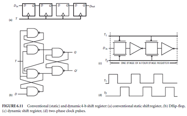
Multiphase clocking is an important technique that can be used to reduce device count in LSI and VLSI circuits. To illustrate the savings that can be realized with the technique, device count is compared for a conventional design of a 4-b shift register employing D flip-flops based on CMOS NAND gates and a 4-b shift register employing two-phase clocks and CMOS technology.
Both designs are shown in Fig. 6.11. Figure 6.11(a) shows the conventional design for the shift register, which employs a single phase clock signal, whereas Fig. 6.11(b) shows the circuit realization of each D flip-flop with CMOS NAND gates (Taub and Schilling, 1977). The device count for each in this design is obtained as follows:
-
5 two-input CMOS NAND gates, 4 transistors each: 20 transistors
-
1 three-input CMOS NAND gate: 6 transistors
-
Number of transistors per D flip-flop: 26
-
Total number of transistors for the 4-b register: 104
The second design, which employs two-phase clocking, is shown in 6.11(c), whereas the nonoverlapping clock signals are shown in Fig. 6.11(d). Note that each flip-flop now consists of two CMOS transmission gates and two CMOS inverters. Thus, there are 8 transmission gates and 8 inverters in the 4-b shift register. Device count for this design is as follows:
-
Number of transistors for 8 transmission gates: 16
-
Number of transistors for 8 CMOS inverters: 16
-
Total number of transistors for the 4-b register: 32
In the preceding example, employing two-phase clocking helped to reduce device count to less than one-third of the requirement in the conventional static design. This gain, however, is partly offset by the need for more complex clocking and the fact that the shift register is now dynamic. To avoid loss of data
due to leakage through off transistors, the clock must run above a minimum frequency. The times required to charge and discharge capacitive loads determine the upper clock frequency.
Increasing Packing Density and Reducing Power Dissipation in MOS Circuits
CMOS gates have much lower power dissipation than NMOS gates. This is a great advantage in LSI and VLSI design. Standard CMOS gates, however, require two transistors per input and, therefore, have higher device count than NMOS gates that require one driving transistor per input, plus one depletion load transistor, irrespective of the number of inputs (Mavor, Jack, and Denyer, 1983). This NMOS feature is put to advantage in applications such as semiconductor memories and programmable logic arrays, which will be discussed later. In addition to requiring a higher device count, it is necessary to isolate the PMOS and NMOS transistors in the CMOS and to employ metal interconnection between their drains, which are of opposite conductivity. Consequently, gate count per chip for NMOS is about half that of CMOS, using the same design rules.
Figure 6.12 shows a CMOS domino logic circuit in which clocking is employed in an unconventional CMOS circuit to provide both high density and low-power dissipation. When T is low, Q1 is off, so there is no path to ground irrespective of the logic levels at the inputs A, B, C, D and E . Q2 is on, so that the parasitic capacitance C1 charges to VDD . When T is high, Q2 is off and Q1 is on. Thus if both A and B , or both C and D, or all of A, B, C , and D are high, a path exists from C1 to ground, and it discharges. Otherwise, C1 remains high (but for slow leakage), and the valid logic ( A B ) + (C + D) appears at the output F . Note that this circuit has only two load PMOS transistors, and only one driving transistor is required for each additional input. Thus, device count is minimized by using complex instead of simple logic functions. Each transistor, except those in the output inverter, may be minimum size, since they
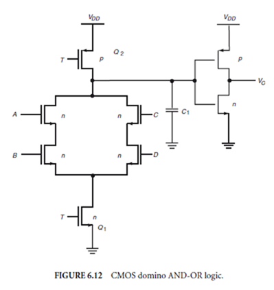 are required only to charge or discharge C1. Power dissipation is low as for standard CMOS, because no steady-state current flows.
Gate Arrays
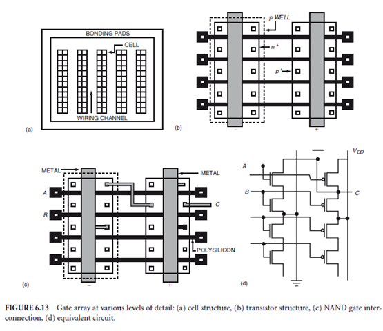
Gate arrays are a category of semicustom integrated circuits typically containing 100 to several thousand gate cells arranged in rows and columns on a chip. The gate cell may be a NAND, NOR, or other gate. Often, each gate cell is a set of components that could be interconnected to form the desired gate or gates. Identical gate cell pattern is employed, irrespective of chip function. Consequently, gate arrays can be largely processed in advance (Reinhard, 1987). Less effort is required for design with gate arrays since only the masks needed for interconnection are required to customize a chip for a particular application.
Figure 6.13 illustrates a gate array in various levels of detail and possible interconnections within a cell. The floor plan of Fig. 6.13(a) shows that there are 10 columns of cells with 10 cells per column, for a total of 100 cells in the chip. The cell layout of Fig. 6.13(b) shows that there are 4 NMOS and 4 PMOS transistors per cell. Thus there are a total of 800 transistors in the chip. The transistor channels are under the polysilicon and inside the diffusion areas. Figure 6.13(c) shows the cell layout with interconnection to form an NAND gate, whereas Fig. 6.13(d) shows the circuit equivalent of a cell.
Because of their simplicity, a significant amount of wiring is required for interconnections in gate arrays. Good computer software is essential for designing interconnections. In practice, wiring channels tend to fill up, so that it is difficult to utilize more than 70% of the cells on a chip (Alexander, 1985). The standard
 cell approach discussed next reduces this problem, to some extent, by permitting use of more complex logic functions or cells.
Standard Cells
In the standard cell approach, the IC designer selects from a library of predefined logic circuits or cells to build the desired circuit. In addition to the basic gates, the cell library usually includes more complex logic circuits such as exclusive-OR, AND-OR-INVERT, flip-flops, adders, read only memory (ROM), etc.
The standard cell approach to design is well suited to automated layout. The process consists of selecting cells from the library in accordance with the desired circuit functions, the relative placement of the cells, and their interconnections. The floor plan for a chip designed by this method is similar to the floor plan for a gate array chip as shown in Fig. 6.13(a). Note, however, that the designer has control over the number and width of wiring channels in this case. Layout for a cell is always the same each time the cell is used, but the cells used and their relative placement is unique to a chip. Thus, every mask level is unique in this approach, and fabrication is more involved and more costly than in the gate array approach (Hodges and Jackson, 1988).
Programmable Logic Devices
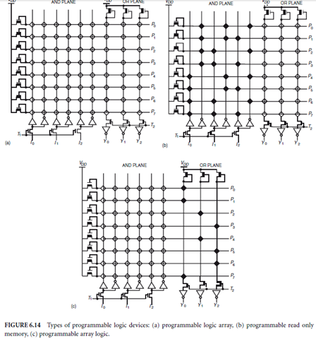
Programmable logic devices (PLDs) are a class of circuits widely used in LSI and VLSI design to implement two-level, sum-of-products, boolean functions. Multilevel logic can be realized with Weinberger arrays or gate matrices (Fabricius, 1990; Weinberger, 1967). Included among PLDs are programmable logic arrays (PLAs), programmable array logic (PAL), and ROM. The AND-OR structure of the PLA, which can be used to implement any two-level function, is the core of all PLDs. The AND-OR function is often implemented with NOR-NOR or NAND-NAND logic.
PLDs have the advantage of leading to highly regular layout structure. The PLD consists of an AND plane followed by an OR plane. The logic function is determined by the presence or absence of contacts or connections at row and column intersections in a single conducting layer. Programming or establishment of appropriate contacts may be accomplished during fabrication. Alternatively, the PLDs may be user programmable by means of fuse links.
Figure 6.14 shows the three types of PLDs. Hollow diamonds at row/column intersections in an AND or OR plane indicates that the plane is programmable. Presence of solid diamonds in some row/column intersections indicate that the logic for that plane is already defined and fixed. The PLD is a PLA if both the AND and OR planes are programmable, a PAL if only the AND plane is programmable, and a ROM if only the OR plane (the decoder in this case) is programmable. Because PLAs are programmable in both planes, they permit more versatile logic realizations than PALs. Also, the PAL can be considered a special case of the PLA. Thus, only the PLA is discussed further.
Programmable Logic Array
PLAs provide an alternative to implementation of combinational logic that results in highly regular layout structures. Consider, for example, a PLA implementation of the following sum of product expressions:
 The PLA has three inputs and three outputs. In terms of the AND and OR planes, the outputs of the AND plane are
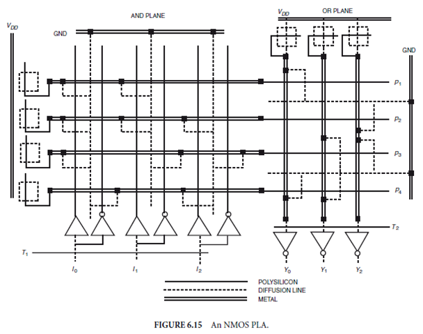
Figure 6.15 shows the logic circuit consisting of the AND and the OR planes. Note that each product line in the AND plane is an NMOS NOR gate with one depletion load; the gate of each driving transistor is controlled by an input line. Likewise, each output line in the OR plane is an NMOS NOR gate with driving transistors whose gates are controlled by the product lines. Thus, the PLA employs a NOR–NOR implementation.
The personality matrix for a PLA (Lighthart, Aarts, and Beenker, 1986) gives a good description of the PLA and how it is to be programmed. The personality matrix Q of the PLA of Fig. 6.15 is given by Eq. (6.15).
The first three columns comprise the AND plane of the matrix, whereas the last three columns comprise the OR plane of the three-input, three-output PLA. In the AND plane, element qij = 0 if a transistor is to link the product line Pi to the input line Ii ; qij = 1 if a transistor is to link Pi to I¯i , and qij is a don’t care if neither input is to be connected to Pi . In the OR plane, qij = 1 if product line Pi is connected to output Y j and 0 otherwise.
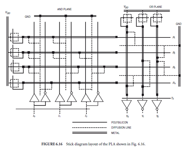
Figure 6.16 shows the stick diagram layout of the PLA circuit of Fig. 6.15, and illustrates how the regular structure of the PLA facilitates its layout. The input lines to each plane are polysilicon, the output lines from each plane are metal, and the sources of driving transistors are connected to ground by diffused lines.
The connecting transistors are formed by grounded, crossing diffusion lines.
Large capacitive loads are encountered in many ways in large integrated circuits. Bonding pads are required for interfacing the chip with other circuits, whereas probe pads are often required for testing. Both present large capacitive loads to their drivers. Interconnections within the chip are by means of metal or polysilicon lines. When long, such lines present long capacitive loads to their drivers. Although regular array structures, such as those of gate arrays, standard cells, and PLAs, are very convenient for semicustom design of LSI and VLSI, they have an inherent drawback with regard to propagation delay. Their row and column lines contact many devices and, hence, are very capacitive. The total delay of a long line may be reduced by inserting buffers along the line to restore the signal. Superbuffers are used for interfacing between small gates internal to the chip and large pad drivers and for driving highly capacitive lines.
Resistance-Capacitance (RC) Delay Lines
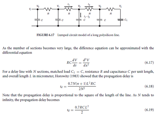
A long polysilicon line can be modeled as a lumped RC transmission line as shown in Fig. 6.17. Let Θx represent the length of a section of resistance R and capacitance C , and Θt be the time required for the signal to propagate along the section. Let ΘV = (Vn−1 − Vn )Θx, where Vn is the voltage at node n. The difference equation governing signal propagation along the line is (Fabricius, 1990)
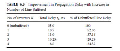
To reduce the total delay restoring inverters can be inserted along a long line. Consider as an example, a 5-mm-long polysilicon line with r = 20 ∆/µm and C = 0.2 f F/µm. It is desired to find the respective propagation delays, if the number of inverters inserted in the line varies from zero to four. The delay of each inverter is proportional to the length of the segment it drives and is given by tI = 0.4 ns when it is driving a 1-mm-long segment. In each case, the inverters used are spaced uniformly along the line. Let
 From Eq. (6.20), the propagation delays can be calculated. The delay for each number of inverters as a percentage of the unbuffered line delay is also computed. The results are tabulated in Table 6.5.
The results in the table show that the propagation delay decreases as the number of inverters is increased. The improvement in propagation delay, however, is less dramatic for each additional inverter than the one preceding it. The designer would stop increasing the number of inverters when the incremental gain no longer justifies an additional inverter. If the number of inverters is even, there is no inversion of the overall signal.
Superbuffers
Propagation delays can be reduced without excessive power consumption by using superbuffers. These are inverting or noninverting circuits that can source and sink larger currents and drive large capacitive
 loads faster than standard inverters. Unlike ratioed NMOS inverters in which the pull-up current drive capability is much less than the pull-down capability, superbuffers have symmetric drive capabilities. A superbuffer consists of a push-pull or totem pole output inverter driven by a conventional inverter. In an inverting superbuffer, the gates of both pull-down transistors in the driving and the totem pole inverters are driven by the input signal whereas the gate of the pull-up transistor in the output totem pole inverter is driven by the complement of the input signal.
An inverting and a noninverting NMOS superbuffer is shown in Fig. 6.18. By designing for an inverter ratio (K R ) of 4, and driving the totem pole pull-up with twice the gate voltage of a standard depletion mode pull-up, the NMOS superbuffer can be rendered essentially ratioless. In standard NMOS inverters, the pull-up transistor has the slower switching speed. Consider the inverting superbuffer of Fig. 6.18(a). When the input voltage goes low, the output voltage of the standard inverter and the gate voltage of Q4 goes high rapidly since the only load it sees is the small gate capacitance of Q4. Thus, the totem pole output switches rapidly. Similar considerations shows that the noninverting super buffer also results in fast switching speeds.
The improvement in drive current capability of the NMOS superbuffer, relative to the standard (deple- tion load) NMOS inverter, can be estimated by comparing the average, output pull-up currents (Fabricius, 1990). The depletion load in the standard NMOS inverter is in saturation for VO < 2 V and in linear region for VO > 2 V. For the pull-up device, VDS = 5 V − VO . Thus, the pull-up transistor is in saturation when it has 3 V < VDS < 5 V and is in the linear region when 0 V < VDS < 3 V. The average current will be estimated by evaluating ID (sat) at VDS = 5 V and ID(lin) at VDS = 2.5 V. Let VTD = −3 V for the depletion mode transistor. Then for the standard NMOS inverter
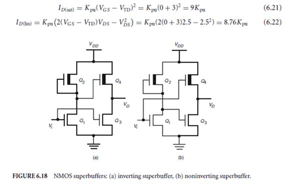 Thus the average pull-up current for the standard NMOS inverter is approximately 8.88Kpu. For the totem pole output of the NMOS superbuffer, the average pull-up current is also estimated from drain currents at VDS = 5 V and 2.5 V. Note that in this case, the pull-up transistor has VG = VDD = 5 V when it is on. Thus, VGS = VDS = 5 V so that it always operates in the linear region. The currents are
The average pull-up current for the totem pole output is 38.12Kpu. The average totem pole pull-up current is approximately 4.3 times the average NMOS pull-up current. Consequently, the superbuffer is roughly ratioless if designed for an inverter ratio of 4.
Output Buffers
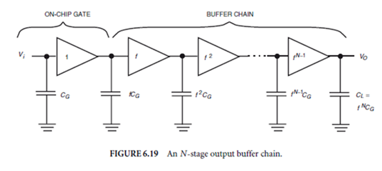
Internal gates on a VLSI chip have load capacitances of about 50 fF or less and typical propagation delays of less than 1 ns. However, the chip output pins have to drive large capacitive loads of about 50 pF or more (Hodges and Jackson, 1988). For MOSFETs, the propagation delay is directly proportional to load capacitance. Thus, using a typical gate on the chip to drive an output pin would result in too long a propagation delay. Output buffers utilize a cascade of inverters of progressively larger drive capability to reduce the propagation delay.
An N-stage output buffer is illustrated in Fig. 6.19. Higher drive capability results from employing transistors of increasing channel width. As the transistor width increases from stage to stage by a factor of f , so does the current drive capability and the input capacitance. If CG is the input or gate capacitance of the first inverter in the buffer, then the second inverter has an input capacitance of f CG and the Nth inverter has an input capacitance of f N−1CG and a load capacitance of f N CG , which is equal to C L , the load capacitance at the output pin. The inverter on the left in the figure is a typical inverter on the chip with an input or gate capacitance of CG and a propagation delay of τ . The first inverter in the buffer has an input capacitance of f CG , but it has a current driving capability f times larger than the on chip inverter. Thus, it has a propagation delay of fτ . The second inverter in the buffer has an input capacitance of f 2CG and an accumulated delay of 2fτ at its output. The Nth inverter has an input capacitance of f N CG , which is equal to the load capacitance at the output pin, and an accumulated propagation delay of Nfτ , which is the overall delay of the buffer.
 By equating to zero the first derivative of tB with respect to f , it is found that tB is minimum at f = e = 2.72, the base of the natural logarithms. This is not a sharp minimum (Moshen and Mead, 1979), and values of f between 2 and 5 do not greatly increase the time delay.
Consider an example in which CG = 50 f F and τ = 0.5 ns for a typical gate driving an identical gate on the chip. Suppose this typical gate is to drive an output pin with load capacitance C L = 55 pF, instead of an identical gate. If an output buffer is used
If the typical chip gate is directly connected to the output pin, the propagation delay is Y τ = 550 ns, which is extremely large compared with the 9.5 ns delay obtained when the buffer is used. This example illustrates the effectiveness of the buffer.
Defining Terms
Cell library: A collection of simple logic elements that have been designed in accordance with a specific set of design rules and fabrication processes. Interconnections of such logic elements are often used in semicustom design of more complex IC chips.
Custom design: A design method that aims at providing a unique implementation of the function needed for a specific application in a way that minimizes chip area and possibly other performance features. Design rules: A prescription for preparing the photomasks used in IC fabrication so that optimum yield is obtained in as small a geometry as possible without compromising circuit reliability. They specify minimum device dimensions, minimum separation between features, and maximum misalignment of features on an IC chip.
Layout: An important step in IC chip design that specifies the position and dimension of features and components on the different layers of masks.
Masks: A set of photographic plates used to define regions for diffusion, metalization, etc., on layers of the IC wafer. Each mask consists of a unique pattern: the image of the corresponding layer.
Standard cell: A predefined logic circuit in a cell library designed in accordance with a specific set of design rules and fabrication processes. Standard cells are typically employed in semicustom design of more complex circuits.
Semicustom design: A design method in which largely predesigned subcircuits or cells are interconnected to form the desired more complex circuit or part of it.
References
Alexander, B. 1985. MOS and CMOS arrays. In Gate Arrays: Design Techniques and Application. ed. J.W. Read. McGraw-Hill, New York.
Fabricius, E.D. 1990. Introduction to VLSI Design. McGraw-Hill, New York.
Hodges, A.D. and Jackson, H.G. 1988. Analysis and Design of Digital Integrated Circuits. McGraw-Hill, New York.
Horowitz, M. 1983. Timing models for MOS pass networks. Proceedings of the IEEE Symposium on Circuits and Systems, pp. 198–201.
Keyes, R.W. 1975. Physical limits in digital electronics. Proc. of IEEE 63:740–767.
Lighthart, M.M., Aarts, E.H.L., and Beenker, F.P.M. 1986. Design for testability of PLAs using statistical cooling. Proceedings of the 23rd ACM/IEEE Design Automation Conference, pp. 339–345, June 29– July 2.
Mavor, J., Jack, M.A., and Denyer, P.B. 1983. Introduction to MOS LSI Design. Addison-Wesley, Reading, MA.
Mead, C.A. and Conway, L.A. 1980. Introduction to VLSI Systems. Addison-Wesley, Reading, MA.
Moshen, A.M. and Mead, C.A. 1979. Delay time optimization for driving and sensing signals on high capacitance paths of VLSI systems. IEEE J. of Solid State Circ. SC-14(2):462–470.
Pucknell, D.A. and Eshroghian, K. 1985. Basic VLSI Design, Principles and Applications. Prentice-Hall, Englewood Cliffs, NJ.
Reinhard, D.K. 1987. Introduction to Integrated Circuit Engineering. Houghton-Mifflin, Boston, MA.
Taub, H. and Schilling, D. 1977. Digital Integrated Circuits. McGraw-Hill, New York.
USC Information Sciences Inst. 1984. MOSIS scalable NMOS process, version 1.0. Univ. of Southern California, Nov., Los Angeles, CA.
USC Information Sciences Inst. 1988. MOSIS scalable and generic CMOS design rules, revision 6. Univ. of Southern California, Feb., Los Angeles, CA.
Weinberger, A. 1967. Large scale integration of MOS complex logic: a layout method. IEEE J. of Solid-State Circ. SC-2(4):182–190.
Further Information
IEEE Journal of Solid State Circuits.
IEEE Proceedings of the Custom Integrated Circuits Conference.
IEEE Transactions on Electron Devices.
Proceedings of the European Solid State Circuits Conference (ESSCIRC).
Proceedings of the IEEE Design Automation Conference.


