Thermal-Related Characteristics of Different Power Switching Devices
The junction temperature of power switching devices is decided by the losses during switching and conducting, as well as the thermal impedance from junction to the ambient [5–7]. Therefore, the characteristics related to the power loss and
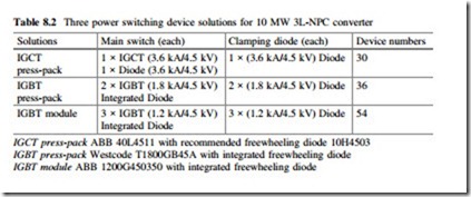
thermal impedance of power switching devices in Table 8.2 are going to be evaluated first.
Switching Loss
The switching loss of the switch (i.e., IGBT or IGCT) is generated when it is turning on and turning off (Eon and Eoff), while the majority switching loss of the diode is generated when it is turning off (Err). As an indicator for the switching loss characteristic, the consumed energy during the switching process (in the unit of Joule) in relation to the current flowing in the switch (Ic) or diode (IF) can be derived from the datasheets of manufacturers.
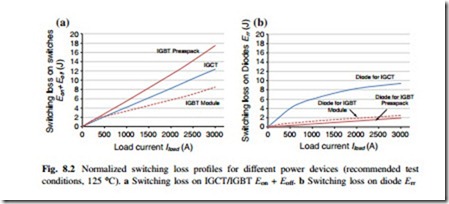
The switching loss profiles of IGCT/IGBT (Eon + Eoff) and diode (Err) for the designed power device solutions are compared in Fig. 8.2a, b respectively. It is noted that, in order to unify and compare solutions with different numbers of parallel devices, the vertical axis in Fig. 8.2 represents the switching loss for only one switch/diode in the parallel device solutions, and the horizontal axis is
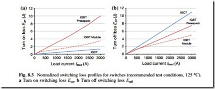
a Turn on switching loss Eon. b Turn off switching loss Eoffnormalized by the load current Iload of the 3L-NPC converter rather than current flowing in the devices (Ic or IF).
It can be seen that for the switches (i.e., IGCT or IGBT), IGBT press-pack has larger total switching loss Eon + Eoff compared to the IGCT press-pack and IGBT module. As for the freewheeling diodes, the IGCT solution shows significantly larger Err compared to the other two IGBT solutions based on press-pack and module packaging technology. This is maybe because the normally used clamping circuit for the IGCT will significantly slow down the rising time of load current during the turning on process, and thereby result in very large reverse recovery charge Qrr on the freewheeling diodes. As for the IGBT module, it shows the lowest overall switching loss either in the switches or in the freewheeling diodes.
When investigating the Eon and Eoff on switch separately, as shown in Fig. 8.3, it can be found that the large switching loss of IGBT press-pack comes from the larger turn on loss Eon. Due to the use of clamping circuit, IGCT can achieve smaller turn on loss Eon, but with the cost of larger switching loss Err in the freewheeling diode, as indicated in Fig. 8.2b, and as can be seen from Fig. 8.3b IGCT shows a large turn off loss Eoff in the switch.
Conduction Voltage and Loss
The conduction loss of the power switching devices is generated when the switch or diode is conducting load current. As an important indicator for the conduction loss characteristic, the conduction voltage of IGCT/IGBT vce or diode vF in relation to the current flowing in switch (Ic) or diode (IF) can be also derived from the data- sheets of manufacturers.
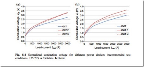
The profiles of vce and vF for the chosen power switching devices with relation to the load current of the 3L-NPC inverter Iload are compared in Fig. 8.4a, b respec- tively. It can be seen that the IGCT and its freewheeling diode show lower conduction voltage compared to the other two IGBT solutions.
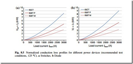
However, different from the switching loss characteristic in Fig. 8.5, the conduction voltage does not directly reflect the conduction loss characteristic of the power switching devices because the current flowing in switch Ic and diode IF have to be also taken into account. In order to better compare the conduction loss performance among different device solutions, a series new profiles are plotted in Fig. 8.5, where the vertical axis is changed to Vce*Ic for switches and VF*IF for diodes. These profiles contain the information of both conduction voltage and switching current, and thereby can directly reflect the conduction loss level of different device solutions. It is noted that the conduction loss characteristics is only for one single device in parallel device solutions.
As it can be seen, although the IGCT solution has the lowest conduction voltage level, it shows the largest conduction loss profile for each device because of much larger current flowing in each device (the current is 3 times of that in each IGBT
module and 2 times of that in each IGBT press-pack as indicated in Table 8.2). Again, the IGBT module solution shows overall lower conduction loss level in each switching device either in the switch or in the diode.
Thermal Resistance
The thermal resistance is another important characteristic which can determine the thermal performances of power switching devices. The thermal resistance from junction to heat sink of each device solution is shown in Fig. 8.6, where the switches and diodes are indicated respectively.
It can be seen that, the thermal resistance of power switching device is closely related to the packaging technology: the press-pack devices IGCT and IGBT have significantly smaller thermal resistance both in the switches and in the freewheeling diodes than the module packaging device “IGBT M”. The freewheeling diodes in all of the three device solutions have significant larger thermal resistance than the corresponding IGBT or IGCT. It is noted that, the major thermal resistance difference between the press-pack and module packaging devices comes from the thermal resistance outside the devices, i.e., from case to heat sink Rth(CH), which is much larger for the IGBT module.
