Power electronic rectifiers (AC/DC converters)
These devices convert a single or a three-phase AC power supply to a smooth DC voltage and current. Simple bi-stable devices, such as the diode and thyristor, can effectively be used for this purpose.
Assumptions
While analyzing power electronic circuits, it is assumed that bi-stable semiconductor devices, such as diodes and thyristors, are the ideal switches, with no losses and minimal forward voltage drop. It will also be assumed that the reactors, capacitors, resistors, and other components of the circuits have ideal linear characteristics with no losses.
Once the operation of a circuit is understood, the imperfections associated with the practical components can be introduced to modify the performance of the power electronic circuit. In power electronics, the operation of any converter is dependent on the switches being turned ON and OFF in a sequence. The current passes through a switch when it is ON and is blocked when it is OFF.
Commutation is the transfer of current from one switch turning OFF, to another turning ON. In a diode rectifier circuit, a diode turns ON and then starts to conduct current when there is a forward voltage across it, i.e., the forward voltage across it becomes positive. This process usually results in the forward voltage across another diode becoming negative, which then turns off and stops conducting current.
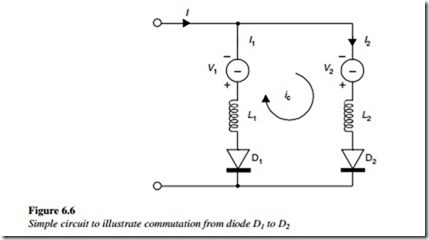
In a thyristor rectifier circuit, the switches additionally need a gate signal to turn them on and off. The factors affecting the commutation are illustrated in the idealized diode circuit in Figure 6.6, which shows two circuit branches, each with its own variable DC voltage source and circuit inductance. Assume, initially, that a current I is flowing through the circuit and that the magnitude of the voltage V1 is larger than V2. Since V1 > V2, diode D1 has a positive forward voltage across it and it conducts a current I1 through its circuit inductance L1. Diode D2 has a negative forward voltage that blocks and carries no current.
Suppose the voltage V2 is increased to a value larger than V1, the forward voltage across diode D2 becomes positive, and it starts to turn on. However, the circuit inductance L1 prevents the current I1 from changing instantaneously and diode D1 will not immediately turn off. Therefore, both the diodes D1 and D2 remain ON for an overlap period called the commutation time Tc .
When both the diodes are turned on, a closed circuit is established which involves both
branches. The effective circuit voltage
Vc = (V2 − V1 ),
called the commutation voltage, drives a circulating current Ic , called the commutation current, through the two branches which have a total circuit inductance of Lc = (L1 + L2 ).
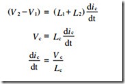
In this idealized circuit, the voltage drop across the diodes and the circuit resistance has been ignored. From the basic electrical theory of inductive circuits, the current Ic increases with time at a rate dependant on the circuit inductance. The magnitude of the commutation current may be calculated from the following equations:
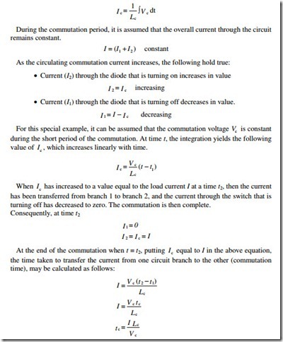
If the commutation starts at a time t1 and finishes at a time t2, the magnitude of the
commutation current
Ic at any time t, during the commutation period, may be calculated, by integrating the above equation from time t1 to t.
It is clear from the equation that the commutation time tc depends on the overall circuit inductance (L1 + L2) and the commutation voltage. From this we can conclude the following:
• A large circuit inductance will result in a long commutation time.
• A large commutation voltage will result in a short commutation time.
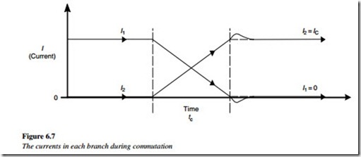
In practice, a number of deviations from this idealized situation occur. The diodes are not ideal and do not turn off immediately when the forward voltage becomes negative. When a conducting diode is presented with a reverse voltage, some reverse current can still flow for a few microseconds, as indicated in Figure 6.7. The current I1 continues to decrease beyond zero to a negative value before returning to zero. This is due to the free charges that must be removed from the PN junction before blocking is achieved.
Even if the commutation time is very short, the commutation voltage of an AC-fed rectifier bridge does not remain constant but changes slightly during the commutation period. An increasing commutation voltage will tend to reduce the commutation time.
Three-phase commutation with six-diode bridge
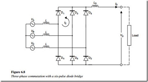
In practical power electronic converter circuits, the commutation follows the same basic sequence outlined above. Figure 6.8 shows a typical six-pulse rectifier bridge circuit to convert three-phase AC currents IA, IB, and IC, to a DC current ID.
This type of circuit is relatively simple to analyze because only two of the six diodes conduct current at any one time. The idealized commutation circuit can easily be identified. In this example, the commutation is assumed to be taking place from diode D1 to D3 in the positive group, while D2 conducts in the negative group.
In power electronic bridge circuits, it is conventional to number the diodes D1 to D6 in the sequence in which they are turned ON and OFF. When VA is the highest voltage and VC the lowest, D1 and D2 are conducting.
Similar to the idealized circuit in Figure 6.8, when VB rises to exceed VA, D3 turns on and commutation transfers the current from diode D1 to D3. As before, the commutation time is dependent on the circuit inductance (L) and the commutation voltage (VB – VA). As can be seen from the six-pulse diode rectifier bridge example in Figure 6.4, the
commutation is usually initiated by external changes.
In this case, the three-phase supply line voltages control the commutation. In other applications, the commutation can also be initiated or controlled by other factors, depending on the type of converter and the application. Therefore, converters are often classified in accordance with the source of the external changes that initiate commutation. In the above example, the converter is said to be line-commutated because the source of the commutation voltage is on the mains supply line. A converter is said to be self- commutated if the source of the commutation voltage comes from within the converter itself. Gate-commutated converters are typical examples of this.
Line-commutated diode rectifier bridge
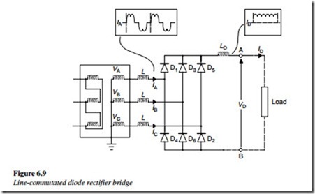
One of the most common circuits used in power electronics is the three-phase line- commutated six-pulse rectifier bridge (Figure 6.9), which comprises of six diodes in a bridge connection. Single-phase bridges will not be covered here because their operation can be deduced as a simplification of the three-phase bridge.
Assumptions
• The supply voltages are stiff and completely sinusoidal
• Commutations are instantaneous and have no recovery problems
• Load currents are completely smooth
• Transformers and other line components are linear and ideal
• There is no volt drop in power electronic switches.
These assumptions are made to gain an understanding of the circuits and to make estimates of currents, voltages, commutation times, etc. In addition, the limiting conditions that affect the performance of the practical converters and their deviation from the ideal conditions will be examined to bridge the gap from the ideal, to the practical.
In the diode bridge, the diodes are not controlled from an external control circuit. Instead, the commutation is initiated externally by the changes that take place in the
supply line voltages, hence the name line-commutated rectifier.
According to convention, the diodes are labeled D1 to D6 in the sequence in which they are turned ON and OFF. This sequence follows the sequence of the supply line voltages.
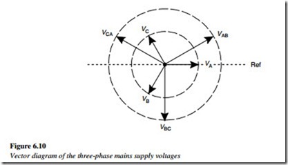
The three-phase supply voltages comprise three sinusoidal voltage waveforms, 120° apart, which rise to their maximum value in the sequence A–B–C. According to convention, the phase-to-neutral voltages are labeled VA, VB, and VC and the phase-to- phase voltages are VAB, VBC and VCA, etc.
These voltages are usually shown graphically as a vector diagram, which rotates counter-clockwise at a frequency of 50 times per second. A vector diagram of these voltages and their relative positions and magnitudes are shown in Figure 6.10. The sinusoidal voltage waveforms, of the supply voltage, may be derived from the rotation of the vector diagram.
The output of the converter is the rectified DC voltage VD, which drives a DC current ID through a load on the DC side of the rectifier. In the idealized circuit, it is assumed that the DC current ID is constant and completely smooth and without ripple. The bridge comprises of two commutation groups, one connected to the positive leg, consisting of diodes D1–D3–D5, and one connected to the negative leg, consisting of the diodes D4–D6– D2. The commutation transfers the current from one diode to another in sequence and each diode conducts the current for 120º of each cycle, as shown in Figure 6.10.
In the upper group, the positive DC terminal follows the highest voltage in the sequence VA–VB–VC via diodes D1–D3–D5. When VA is near its positive peak, the diode D1 conducts and the voltage of the positive DC terminal follows VA. The DC current flows through the load and returns via one of the lower group diodes. With the passage of time, VA reaches its sinusoidal peak and starts to decline. At the same time, VB rises and eventually reaches a point, when it becomes equal to and starts to exceed VA. At this point, the forward voltage across diode D3 becomes positive and it starts to turn on. The commutating voltage in this circuit, VB–VA starts to drive an increasing commutation current though the circuit inductances and the current through D3 start to increase, as the current in D1 decreases. In a sequence of events similar to that described above, the commutation takes place and the current is transferred from diode D1 to diode D3. At the end of the commutation period, the diode D1 is blocked and the positive DC terminal follows VB until the next commutation takes place, to transfer the current to diode D5. After the diode D5, the commutation transfers the current back to D1 and the cycle is repeated.
In the lower group, a similar sequence of events takes place, but here the negative voltages and the current flow from the load back to the mains. Initially, D2 is assumed to be conducting when VC is more negative than VA. As time progresses, VA becomes equal to VC and then becomes more negative. The commutation takes place and the current is transferred from diode D2 to D4. Diode D2 turns off and D4 turns on. The current is later transferred to diode D6, then back to D2 and the cycle is repeated.
In Figure 6.10, the conducting periods of the diodes in the upper and lower groups are shown over several cycles of the three-phase supply. This shows that only two diodes conduct current at any time (except during the commutation period, which is assumed to be infinitely short) and that each of the six diodes conduct for only one portion of the cycle in a regular sequence. The commutation takes place alternatively in the top group and the lower group.
The DC output voltage VD is not a smooth voltage and consists of portions of the phase- to-phase voltage waveforms. For every cycle of the 50 Hz AC Waveform (20 ms), the DC voltage VD comprises portions of six voltage pulses, VAB, VAC, VBC, VBA, VCA, VCB, etc., hence the name, six-pulse rectifier bridge.
The average magnitude of the DC voltage may be calculated from the voltage waveform shown in Figure 6.10. The average value is obtained by integrating the voltage over one of the repeating 120º portions of the DC voltage curve. This integration yields an average magnitude of the voltage VD as follows:
VD = 1.35 × (RMS phase − Phase voltage)
VD = 1.35 × V RMS
For example, if VRMS = 415 V, then VD = 560 V DC. When there is a sufficient inductance in the DC circuit, then DC current ID will be steady and the AC supply current will comprise of segments of DC current from each diode in sequence.
As an example, the current in the A-phase is shown in Figure 6.11. The non-sinusoidal current that flows in each phase of the supply mains can affect the performance of any other AC equipment connected. In practice, to ensure that the diode reverse blocking voltage capability is properly specified, it is necessary to know the magnitude of the reverse blocking voltage that appears across each of the diodes to the supply line that is designed to operate with sinusoidal waveforms.
Theoretically, the maximum reverse voltage across a diode is equal to the peak of the phase–phase voltage. For example, the reverse voltage VCA and VCB appear across diode D5 during the blocking period. In practice, a safety factor of 2.5 is commonly used for specifying the reverse-blocking capability of diodes and other power electronic switches. On a rectifier bridge fed from a 415 V power supply, the reverse blocking voltage Vbb of the diode must be higher than 2.5 × 440 V = 1100 V. Therefore, it is common practice to use diodes with a reverse-blocking voltage of 1200 V.
(iii) If the control fuse is OK, check whether the overload relay has tripped.
Check this with the help of a multimeter. Check voltage between the neutral terminal and the outgoing terminal of the overload relay contact, connected
to the stop pushbutton. If the overload relay has not tripped and the multimeter shows that the control voltage between the two points is OK, then go to point (iv).
(iv) Check the control voltage at the stop pushbutton outgoing terminal to the start pushbutton. If the voltage is OK, then go to point (v).
(v) If two NO contacts are connected in parallel to each other, and the motor runs only when the start pushbutton is pressed, it indicates that, the NO contact of the main contactor must close as soon as the main contactor is switched on. It also indicates that the contactor that holds the control circuit on is not closing. The wires connected in parallel from the NO contact to the start pushbutton NO contact may be closed, or the NO contact of the main contactor is not closed, due to a faulty contact. To confirm this, take a loop of insulated wire, and short the contact K1; if the motor starts, it confirms that the NO contact is faulty. Change the NO contact block of the main contactor.
If the motor runs and trips after 2 min, to troubleshoot this perform the following steps:
(i) Check the control supply (L1), check control voltage between L1 and neutral (N).
(ii) Check the control fuse (F3) with the multimeter. If the control fuse (F3) is blown change the fuse and restart the motor. The motor must start if the control fuse (F3) blown was the only problem.
(iii) If the control fuse is OK, check whether the overload relay has tripped.
Check this with the help of a multimeter, by checking the voltage between the neutral terminal and the outgoing terminal of the overload relay contact connected to the stop pushbutton. If the overload relay has tripped, you will
not get control voltage between the two points. Reset the overload relay and look into the reasons for which the motor tripped on overload.
If there is a voltage between the two points, look for a loose contact or loose wiring at the subsequent contacts in the control circuits.

