The 555 Timer
The 555 timer is an eight-pin integrated circuit that has become one of the most popular electronic devices used in industrial electronic circuits. The reason for the 555’s popularity is its tremendous versatility. The 555 timer is used in circuits that require a time delay function, and it is also used as an oscillator to provide the pulses needed to operate computer circuits.
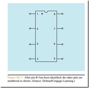
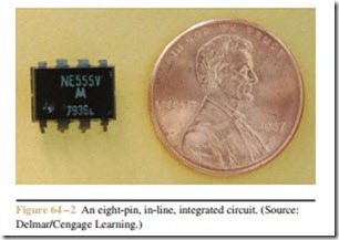
The 555 timer is most often housed in an eight-pin, in-line integrated circuit (IC) (Figures 64 – 1 and 64 – 2). This package has a notch at one end, or a dot by one pin, which is used to identify pin #1. Once pin #1 has been identified, the other pins are numbered as shown in Figure 64 – 1. The 555 timer operates on voltages that range from about 3 to 16 volts. Following is an explanation of each pin and its function:
Pin #1 Ground—This pin is connected to circuit ground.
Pin #2 Trigger—Pin #2 must be connected to a volt- age that is less than 1⁄3 Vcc (the applied voltage) to trigger the unit. This usually is done by
connecting pin #2 to ground. The connection to (For the following explanation, assume that pin #2 is connected to pin #6. This permits the unit to be retriggered by the discharge each time it turns on and discharges the capacitor to 1⁄3 the value of Vcc.)
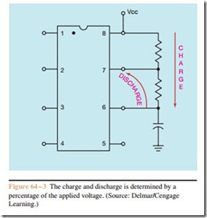
The 555 timer operates on a percentage of the applied voltage. This permits the time setting to remain constant even if the applied voltage changes. For ex- ample, when the capacitor connected to pin #6 reaches 2⁄3 of the applied voltage, the discharge turns on and discharges the capacitor until it reaches 1⁄3 of the applied voltage. If the applied voltage of the timer is connected to 12 volts DC, 2⁄3 of the applied voltage is 8 volts and 1⁄3 is 4 volts. This means that when the voltage across the capacitor connected to pin #6 reaches 8 volts, pin #7 will turn on until the capacitor is discharged to 1⁄3 the value of Vcc, or 4 volts, and will then turn off (Figure 64 – 3).
1⁄3 Vcc or ground must be momentary. If pin #2 If the voltage is lowered to 6 volts at Vcc,
2⁄3 of the
is not removed from ground, the unit will not operate.
Pin #3 Output—The output turns on when Pin #2 is triggered and turns off when the discharge is turned on.
Pin #4 Reset—When this pin is connected to Vcc, it permits the unit to operate. When it is connected to ground, it activates the discharge and keeps the timer from operating.
Pin #5 Control Voltage—If this pin is connected to Vcc through a variable resistor, the on time is longer, but the off time is not affected. If pin #5 is connected to ground through a variable reapplied voltage is 4 volts and 1⁄3 of the applied voltage is 2 volts. Pin #7 will now turn on when the voltage across the capacitor connected to pin #6 reaches 4 volts and will turn off when the voltage across the capacitor drops to 2 volts.
The formula for a RC time constant is (Time = Resistance X Capacitance). Notice that there is no men- tion of voltage in the formula. This means that it will take the same amount of time to charge the capacitor regardless of whether the circuit is connected to 12 volts
Figure 64 – 3 The charge and discharge is determined by a percentage of the applied voltage. (Source: Delmar/Cengage Learning.)
or to 6 volts. If the time it takes for the voltage of the capacitor connected to pin #6 to reach 2⁄3 of Vcc when the timer has an applied voltage of 12 volts is measured, it will be the same as the amount of time it takes when the applied voltage is only 6 volts. The timing of the circuit remains the same even if the voltage changes.
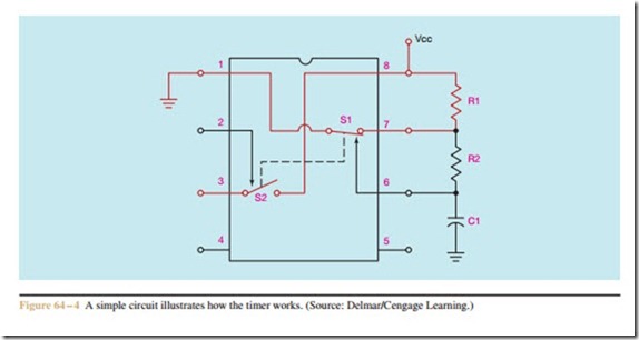
The circuit shown in Figure 64 – 4 is used to ex- plain the operation of the 555 timer. In Figure 64 – 4, a normally closed switch, S1, is connected between the discharge, pin #7, and the ground, pin #1. A normally open switch, S2, is connected between the output, pin
#3, and Vcc, pin #8.
The dotted line drawn between these two switches shows mechanical connection. This means that these switches operate together. If S1 opens, S2 closes at the same time. If S2 opens, S1 closes. Pin #2, the trigger, and pin #6, the threshold, are used to control these switches. The trigger can close switch S2, and the threshold can close S1.
To begin the analysis of this circuit, assume that switch S1 is closed and switch S2 is open as shown in Figure 64 – 4. When the trigger is connected to a volt- age that is less than 1⁄3 of Vcc, it causes switch S2 to close and switch S1 to open. When switch S2 closes, voltage is supplied to the output at pin #3. When switch S1 opens, the discharge is no longer connected to ground, and capacitor C1 begins to charge through resistors R1 and R2. When the voltage across C1 reaches 2⁄3 of Vcc, the threshold, pin #6, causes switch S1 to close and switch S2 to open. When switch S2 opens,
the output turns off. When switch S1 closes, the dis- charge, pin #7, is connected to ground. Capacitor C1 then discharges through resistor R2. The timer will re- main in this position until the trigger is again connected to a voltage that is less than 1⁄3 of Vcc.
If the trigger is connected permanently to a voltage less than 1⁄3 of Vcc, switch S2 will be held closed and switch S1 will be held open. This, of course, will stop the operation of the timer. As stated previously, the trigger must be a momentary pulse, not a continuous connection, in order for the 555 timer to operate.
Circuit Applications
The Oscillator
The 555 timer can perform a variety of functions. It is commonly used as an oscillator. The 555 timer has become popular for this application because it is so easy to use.
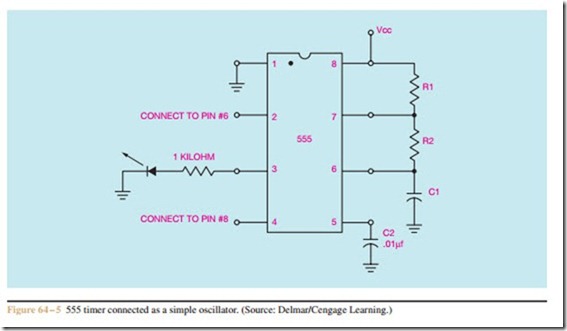
The 555 timer shown in Figure 64 – 5 has pin #2 connected to pin #6. This permits the timer to retrigger itself at the end of each time cycle. When the applied voltage is turned on, capacitor C1 is discharged and has a voltage of 0 volts across it. Since pin #2 is connected to pin #6, and the voltage at that point is less than 1⁄3 of Vcc, the timer will trigger. When the timer is triggered, two things happen at the same time: the output turns on, and the discharge turns off. When the discharge at
pin #7 turns off, capacitor C1 charges through resistors R1 and R2. The amount of time it takes for capacitor C1 to charge is determined by the capacitance of the capacitor and the combined resistance of R1 and R2.
When capacitor C1 is charged to a voltage that is 2⁄3 of Vcc, the output turns off, and the discharge at pin #7 turns on. When the discharge turns on, capacitor C1 discharges through resistor R2 to ground. The amount of time it takes C1 to discharge is determined by the capacitance of capacitor C1 and the resistance of R2. When capacitor C1 is discharged to a voltage that is 1⁄3 of Vcc, the timer is retriggered by pin #2, causing the out- put to turn on and the discharge to turn off. When the dis- charge turns off, capacitor C1 begins charging again.
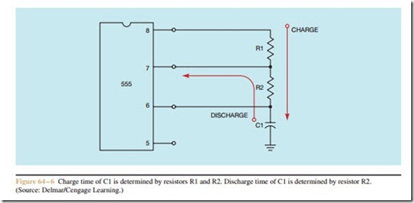
The amount of time required to charge capacitor C1 is determined by the combined resistance of R1 and R2. The discharge time, however, is determined by the value of R2 (Figure 64 – 6).
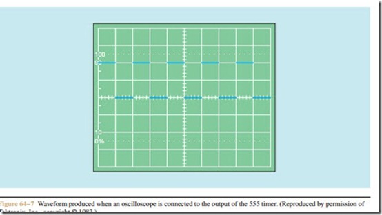
Since the timer’s output is turned on while capacitor C1 is charging, and turned off while C1 is discharging, the on time of the output is longer than the off time. If the value of resistor R2 is much greater than the value of resistor R1, this condition is not too evident. For example, if resistor R1 has a value of 1 kilohm and R2 has a value of 100 kilohms, the resistance connected in series with the capacitor during charging is 101 kilo hms. The resistance connected in series with the capacitor during discharge is 100 kilohms. In this circuit, the difference between the charge time and the discharge time of the capacitor is 1%. If an oscilloscope is connected to the output of the timer, a waveform similar to the waveform shown in Figure 64 – 7 will be seen.
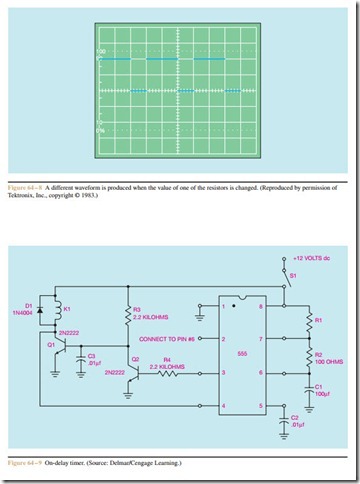
Assume that the value of resistor R1 is changed to 100 kilohms and the value of resistor R2 remains at 100 kilohms. In this circuit, the resistance con- nected in series with the capacitor during charging is 200 kilohms. The resistance connected in series with the capacitor during discharge, however, is 100 kilohms. Therefore, the discharge time is 50% of the charge time. This means that the output of the timer will be turned on twice as long as it will be turned off. An oscilloscope connected to the output of the timer would display a waveform similar to the one shown in Figure 64 – 8.
Although this condition can exist, the 555 timer has a provision for solving the problem. Pin #5, the control voltage pin, can give complete control of the output voltage. If a variable resistor is connected between pin #5 and Vcc, the on time of the output can be lengthened to any value desired. If a variable resistor is connected between pin #5 and ground, the on time of the output can be shortened to any value desired. Since the on time of the timer is adjusted by connecting resistance to pin #5, the off time is set by the values of C1 and R2.
The output frequency of the unit is determined by the values of capacitor C1 and resistors R1 and R2. The 555 timer will operate at almost any frequency desired. It is used in many industrial electronic circuits that require the use of a square wave oscillator.
The On-Delay Timer
In this circuit, the 555 timer is used to construct an on-delay relay. The 555 produces accurate time delays that can range from seconds to hours depending on the values of resistance and capacitance used in the circuit. In Figure 64 – 9, transistor Q1 is used to switch relay coil K1 on or off. A transistor is used to control the re- lay because the 555 timer may not be able to supply the current needed to operate it.
Transistor Q2 is used as a stealer transistor to steal the base current from transistor Q1. As long as transistor Q2 is turned on by the output of the timer, transistor Q1 is turned off.
Capacitor C3 is connected from the base of transistor Q1 to ground. Capacitor C3 acts as a short time- delay circuit. When Vcc is turned on by switch S1, capacitor C3 is discharged. Before transistor Q1 can be turned on, capacitor C3 must be charged through resistor R3. This charging time is only a fraction of a second, but it ensures that transistor Q1 will not turn on before the output of the timer can turn transistor Q2 on. Once transistor Q2 has been turned on, it will hold transistor Q1 off by stealing its base current.
Diode Dl is used as a kickback, or freewheeling, diode to kill the spike voltage induced into the coil of relay K1 when switch S1 is opened. Resistor R3 limits the base current to transistor Q1 and resistor R4 limits the base current to transistor Q2.
Pin #4, the reset pin, is used as a latch in this circuit. When power is applied at Vcc, transistor Q1 is turned off. Since transistor Q1 is off, most of the applied voltage is dropped across the transistor, causing about 12 volts to appear at the collector of the transistor. Since pin #4 is connected to the collector of transistor Q1, 12 volts is applied to pin #4. For the timer to operate, pin #4 must be connected to a voltage that is greater than 2⁄3 of Vcc. When pin #4 is connected to a voltage that is less than 1⁄3 of Vcc, it turns on the discharge and keeps the timer from operating. When transistor Q1 turns on, the collector of the transistor drops to ground or 0 volts. Pin #4 is also connected to ground, which prevents the timer from further operation. Since the timer can no longer operate, the output remains turned off, which permits transistor Q1 to remain turned on.
Capacitor C1 and resistors R1 and R2 are used to set the amount of time delay. Resistor R2 should be kept at a value of about 100 ohms. The job of resistor R2 is to limit the current when capacitor C1 discharges. Resis- tor R2 has a relatively low value to enable capacitor C1 to discharge quickly. The time setting can be changed by changing the value of resistor R1.
To understand the operation of the circuit, assume that switch S1 is open and all capacitors are discharged. When switch S1 is closed, pin #2, which is connected to 0 volts, triggers the timer. When the timer is triggered, the output activates transistor Q2, which steals the base current from transistor Q1. Transistor Q1 re- mains off as long as transistor Q2 is on. When capacitor C1 has been charged to 2⁄3 of Vcc, the discharge turns on and the output of the timer turns off. When the output turns transistor Q2 off, transistor Q1 is supplied with base current through resistor R3 and turns on relay coil K1. When transistor Q1 is turned on, the voltage applied to the reset pin, #4, is changed from 12 volts to 0 volts. This causes the reset to lock the discharge on and the output off. Therefore, when transistor Q1 is turned on, switch S1 must be reopened to reset the circuit.
Review Questions
1. How is pin #1 of an in-line, integrated circuit identified?
2. A 555 timer is connected to produce a pulse at the output once each second. The timer is connected to 12 volts DC. If the voltage is reduced to 8 volts DC, the 555 will continue to operate at the same pulse rate. Explain why the timer will operate at the same pulse rate when the voltage is reduced.
3. What is the range of voltage the 555 timer will operate on?
4. Explain the function of the control voltage, pin
#5, when the timer is being used as an oscillator.
5. Explain what happens to the output and discharge pins of the 555 timer when the trigger, pin #2, is connected to a voltage that is less than 1⁄3 of Vcc.
6. Explain what happens to the output and discharge pins when the threshold, pin #6, is connected to a voltage that is greater than 2⁄3 of Vcc.
7. Refer to figure 64 – 6. The values of what compo- nents determine the length of time the output will be turned on?
8. The values of what components determine the amount of time the output will remain turned off?
9. Explain the operation of pin #4 on the 555 timer.
10. What is a stealer transistor?
